NSC DM9338J-883 Datasheet

TL/F/9794
9338/DM9338 8-Bit Multiple Port Register
June 1989
9338/DM9338 8-Bit Multiple Port Register
General Description
The DM9338 is an 8-bit multiple port register designed for
high speed random access memory applications where the
ability to simultaneously read and write is desirable. A common use would be as a register bank in a three address
computer. Data can be written into any one of the eight bits
and read from any two of the eight bits simultaneously.
Connection Diagrams
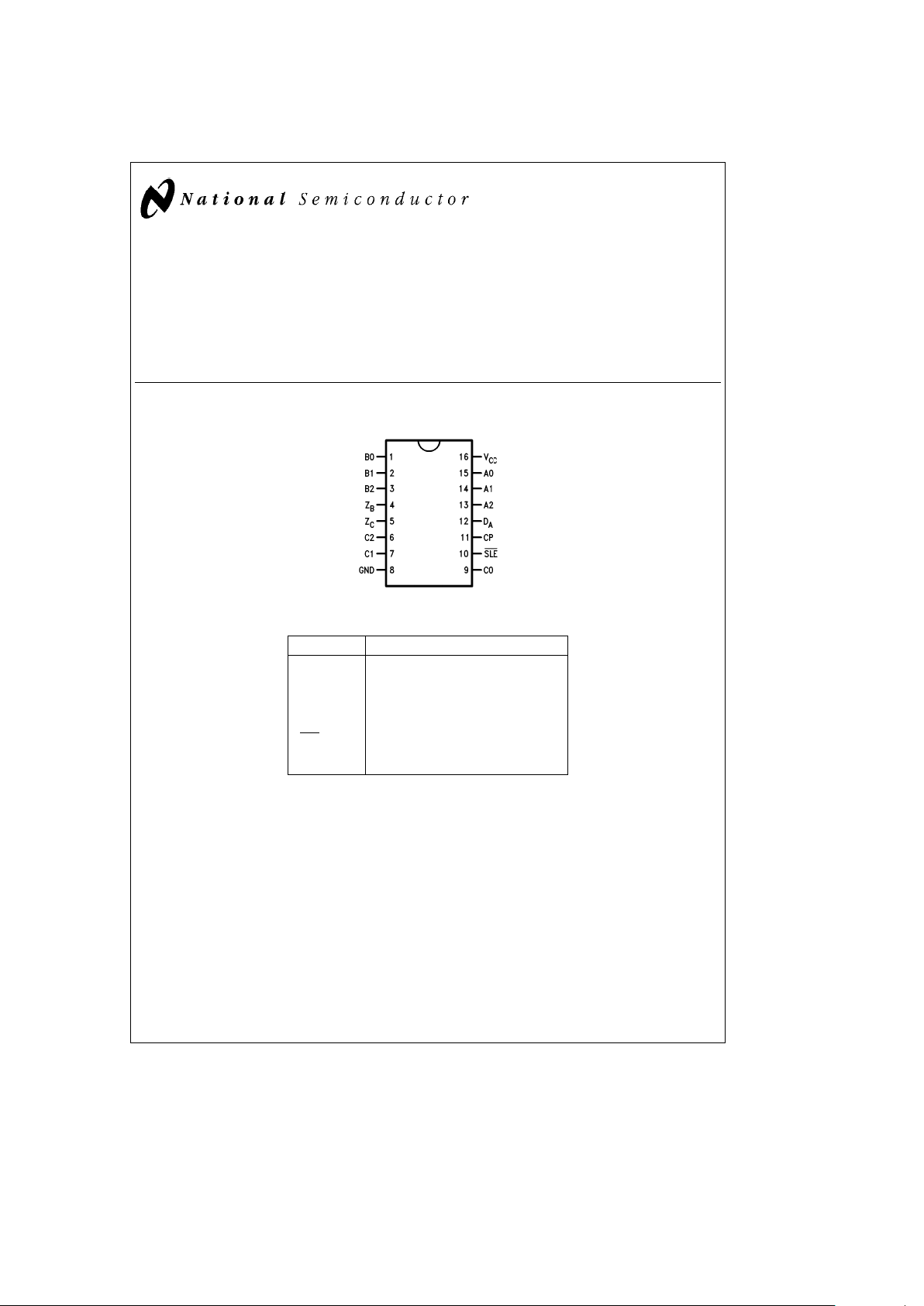
Dual-In-Line Package
TL/F/9794– 1
Order Number 9338DMQB, 9338FMQB or DM9338N
See NS Package Number J16A, N16E or W16A
Pin Names Description
A0–A2 Write Address Inputs
D
A
Data Input
B0–B2 B Read Address Inputs
C0–C2 C Read Address Inputs
CP Clock Pulse Input (Active Rising Edge)
SLE
Slave Enable Input (Active LOW)
Z
B
B Output
Z
C
C Output
FASTÉand TRI-STATEÉare registered trademarks of National Semiconductor Corporation.
C
1995 National Semiconductor Corporation RRD-B30M115/Printed in U. S. A.

Absolute Maximum Ratings (Note)
If Military/Aerospace specified devices are required,
please contact the National Semiconductor Sales
Office/Distributors for availability and specifications.
Supply Voltage 7V
Input Voltage 5.5V
Operating Free Air Temperature Range
Military
b
55§Ctoa125§C
Commercial 0
§
Ctoa70§C
Storage Temperature Range
b
65§Ctoa150§C
Note:
The ‘‘Absolute Maximum Ratings’’ are those values
beyond which the safety of the device cannot be guaranteed. The device should not be operated at these limits. The
parametric values defined in the ‘‘Electrical Characteristics’’
table are not guaranteed at the absolute maximum ratings.
The ‘‘Recommended Operating Conditions’’ table will define
the conditions for actual device operation.
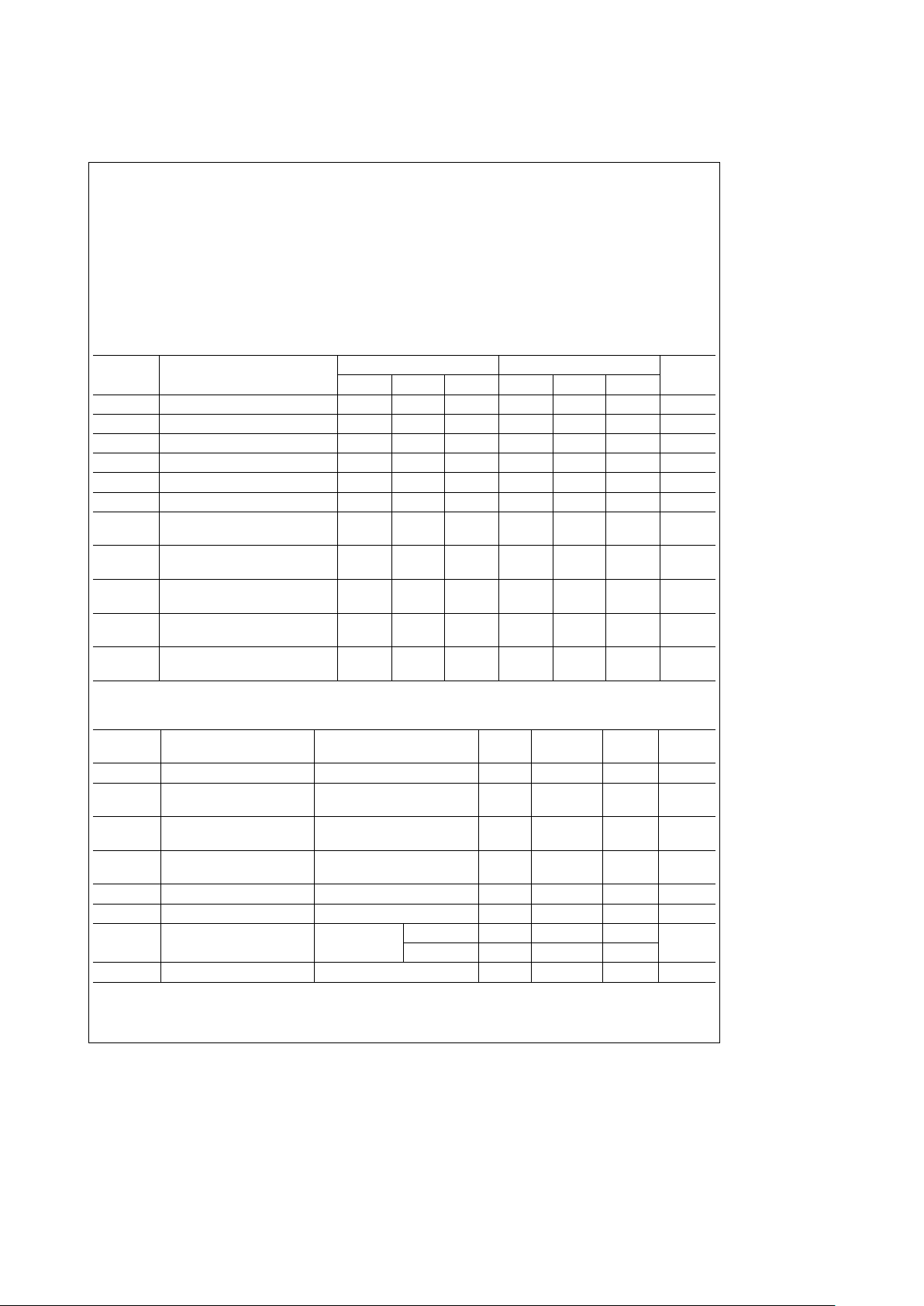
Recommended Operating Conditions
Symbol Parameter
Military Commercial
Units
Min Nom Max Min Nom Max
V
CC
Supply Voltage 4.5 5 5.5 4.75 5 5.25 V
V
IH
High Level Input Voltage 2 2 V
V
IL
Low Level Input Voltage 0.8 0.8 V
I
OH
High Level Output Current
b
0.8
b
0.8 mA
I
OL
Low Level Output Current 16 16 mA
T
A
Free Air Operating Temperature
b
55 125 0 70
§
C
ts(H) Setup Time HIGH or LOW 20 20
ns
t
s
(L) DAto CP 12 12
th(H) Hold Time HIGH or LOW 0 0
ns
th(L) DAto CP
b
8.0
b
8.0
ts(H) Setup Time HIGH or LOW 10 10
ns
t
s
(L) Anto CP 10 10
th(H) Hold Time HIGH or LOW 0 0
ns
t
h
(L) Anto CP 0 0
tw(H) CP Pulse Width HIGH or LOW 23 23
ns
t
w
(L) 13 13
Electrical Characteristics
Over recommended operating free air temperature range (unless otherwise noted)
Symbol Parameter Conditions Min
Typ
Max Units
(Note 1)
V
I
Input Clamp Voltage V
CC
e
Min, I
I
eb
12 mA
b
1.5 V
V
OH
High Level Output Voltage V
CC
e
Min, I
OH
e
Max
2.4 3.4 V
V
IL
e
Max
V
OL
Low Level Output Voltage V
CC
e
Min, I
OL
e
Max
0.2 0.4 V
V
IH
e
Min
I
I
Input Current@Max V
CC
e
Max, V
I
e
5.5V
1mA
Input Voltage
I
IH
High Level Input Current V
CC
e
Max, V
I
e
2.4V 27 mA
I
IL
Low Level Input Current V
CC
e
Max, V
I
e
0.4V
b
1.1 mA
I
OS
Short Circuit V
CC
e
Max MIL
b
10
b
70
mA
Output Current (Note 2)
COM
b
10
b
70
I
CC
Supply Current V
CC
e
Max 135 mA
Note 1: All typicals are at V
CC
e
5V, T
A
e
25§C.
Note 2: Not more than one output should be shorted at a time.
2
 Loading...