Features
■
41MSPS
■
Wide dynamic range
SFDR: 72dBc
SNR: 64dB
■
Low power dissipation: 660mW
■
Ground centered,
DC-coupled analog input
■
Excellent PSRR: >60dB
■
Very small package: 28-pin SSOP
■
Low cost
Applications
■
Cellular base-stations
■
Digital communications
■
Infrared/CCD imaging
■
IF sampling
■
Electro-optics
■
Instrumentation
■
Medical imaging
■
High definition video
General Description
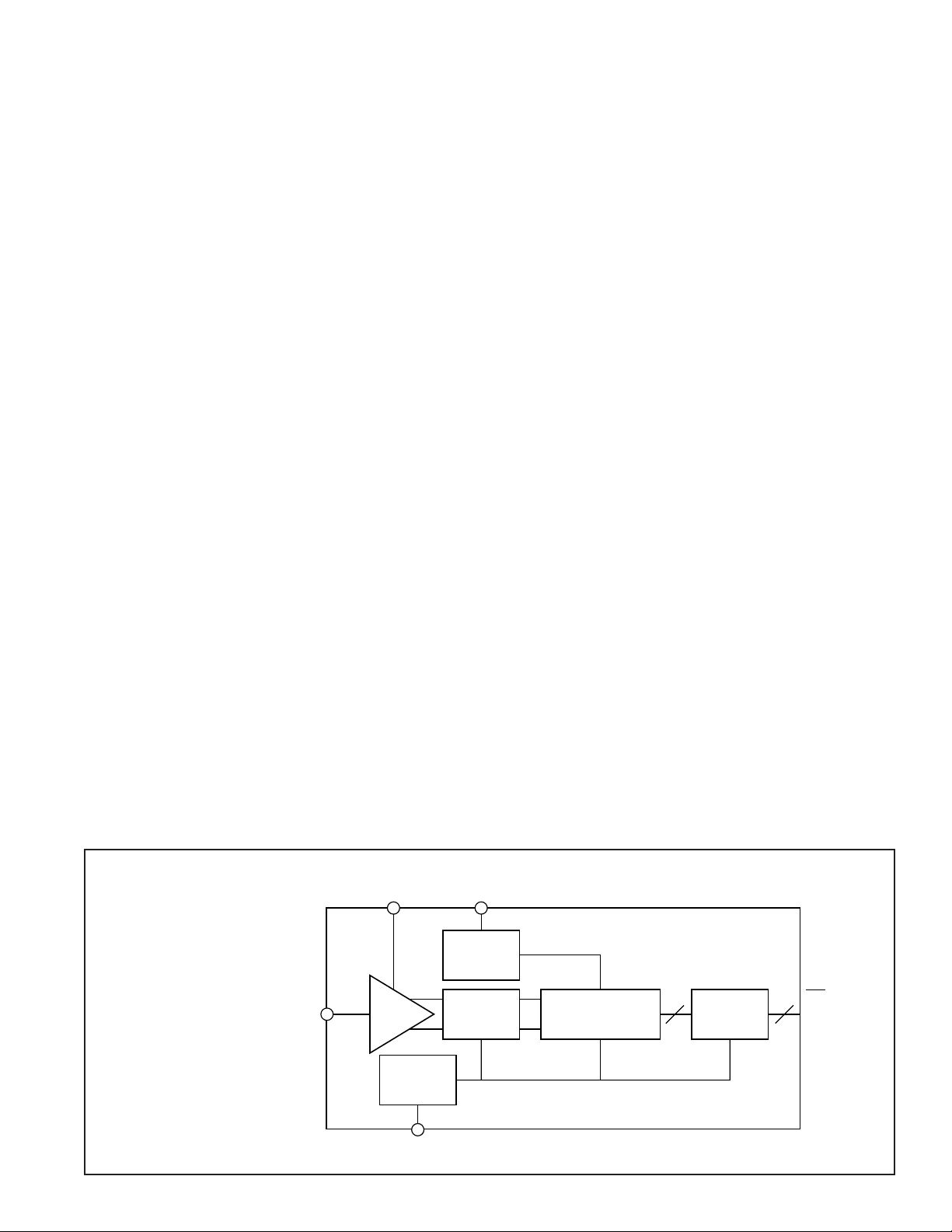
The CLC952 is a complete monolithic 12-bit 41MSPS analog-todigital converter system. Fabricated from a 0.8µm BiCMOS
process, the CLC952’s on-chip features include a very
linear wideband track-and-hold, bandgap voltage reference and a
proprietary 12-bit multi-stage quantizer. The CLC952 has been
designed for wideband digital communications receivers and
features a 72dBc spurious-free dynamic range (SFDR) and 64dB
signal-to-noise ratio (SNR).
The CLC952 operates from a standard ±5V power supply and
features excellent noise isolation with its >60dB power-supply
rejection ratio (PSRR). All digital control functions and output
registers are TTL compatible. The CLC952AC operates over the
commercial temperature range (0°C to 70°C), and the CLC952AJ
operates over the industrial temperature range (-40°C to 85°C)
version. The CLC952 is available in a 28-pin SSOP that provides
an extremely small footprint for reduced board space. National
Semiconductor thoroughly tests each part to verify full
compliance with guaranteed specifications.
CLC952
12-bit, 41MSPS Monolithic A/D Converter
N
September 1997
CLC952
12-bit, 41MSPS Monolithic A/D Converter
12-bit Subranging
Quantizer
T/H
Amplifier
TTL Output
Buffer
Timing
Generator
2.4V Voltage
Reference
Input
Amp
D11 MSB
•
•
D0 LSB
V
in
V
REF
Offset
Adjust
ENCODE
© 1997 National Semiconductor Corporation http://www.national.com
Printed in the U.S.A.
CLC952
Block Diagram

http://www.national.com 2
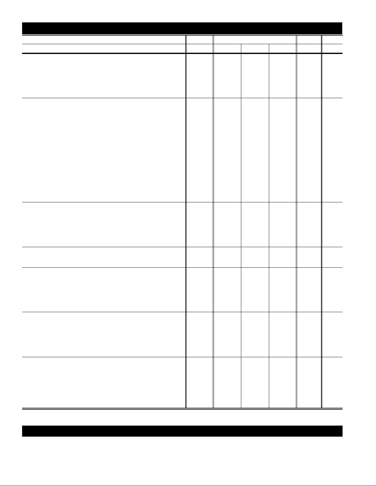
PARAMETERS CONDITIONS TEMP RATINGS UNITS NOTES
Note 4 MIN TYP MAX
DYNAMIC PERFORMANCE
small-signal bandwidth V
in
= 1/4FS +25°C 185 MHz
large-signal bandwidth V
in
= FS +25°C 180 MHz
slew rate +25°C 357 V/µs
overvoltage recovery time V
in
= 1.5FS (0.01%) +25°C 5 ns
effective aperture delay +25°C 1.6 ns
aperture jitter +25°C 4 ps(rms)
NOISE AND DISTORTION (40.96MSPS)
signal-to-noise ratio (w/o harmonics)
2.0MHz FS +25°C 60 64 dB 1
FS Full 61 dB
9.67MHz FS +25°C 60 64 dB 1
FS Full 61 dB
19.5MHz FS +25°C 60 62 dB 1
FS Full 60 dB
spurious-free dynamic range
2.0MHz FS-1dB +25°C 64 72 dBc 1
FS-1dB Full 71 dBc
9.67MHz FS-1dB +25°C 61 69 dBc 1
FS-1dB Full 68 dBc
19.5MHz FS-1dB +25°C 60 67 dBc 1
FS-1dB Full 66 dBc
intermodulation distortion
19.49MHz (f
1
), 19.9MHz (f2) FS-7dB +25°C 75 dBFS
DC ACCURACYAND PERFORMANCE
differential non-linearity DC; FS +25°C 1.4 LSB
integral non-linearity DC; FS +25°C 3.0 LSB
bipolar offset error +25°C 5.1 mV
bipolar offset error Full 25.0 mV 3
bipolar gain error +25°C -4.5 %FS
bipolar gain error Full 15.0 %FS 3
ANALOG INPUT AND PERFORMANCE
analog input resistance +25°C 500 Ω
analog input capacitance +25°C 2 pF
DIGITAL INPUTS
input voltage logic LOW Full 0.8 V 1,3
logic HIGH Full 2.0 V 1,3
input current logic LOW Full 0 5 µA 1,3
logic HIGH Full 4.0 25 µA 1,3
output voltage logic LOW Full 0.8 V 1,3
logic HIGH Full 2.4 V 1,3
TIMING
maximum conversion rate Full 40.96 MSPS 1,3
minimum conversion rate Full 3.0 MSPS 3
pulse width high Full 12.2 15 ns 3
pulse width low Full 10.5 12.2 ns 3
pipeline delay Full 1.0 clk cycle 3
output propagation delay +25°C 15 ns
POWER REQUIREMENTS
+5V supply current 41MSPS +25°C 54 70 mA 1
+5V supply current 41MSPS Full 70 mA 3
-5V supply current 41MSPS +25°C 78 100 mA 1
-5V supply current 41MSPS Full 100 mA 3
nominal power dissipation 41MSPS +25°C 660 mW
V
EE
power supply rejection ratio +25°C 72 dB
V
CC
power supply rejection ratio +25°C 60 dB
Min/max ratings are based on product characterization and simulation. Individual parameters are tested as noted. Outgoing quality levels are
determined from tested parameters.
CLC952 Electrical Characteristics
(VCC= +5V, VEE= -5V, 40.96MSPS; unless specified)
Notes
1) These parameters are 100% tested at 25°C.
2) Typical specifications are the mean values of the distributions of
deliverable converters tested to date.
3) Min/max data over temperature is based on the 5 sigma limit for
deliverable converters tested to date.
4) Full temperature range is 0°C to +70°C for AC, -40°C to +85°C for AJ.

Absolute Maximum Ratings
positive supply voltage (VCC) -0.5V to +6V
negative supply voltage (VEE) +0.5V to -6V
differential voltage between any two grounds <200mV
analog input voltage range V
EE
toV
CC
digital input voltage range -0.5V to +V
CC
output short circuit duration (one-pin to ground) infinite
junction temperature 175°C
storage temperature range -65°C to 150°C
lead solder duration (+300°C) 10sec
Note: Absolute maximum ratings are limiting values, to be applied individually,
and beyond which the serviceability of the circuit may be impaired. Functional
operability under any of these conditions is not necessarily implied. Exposure to
maximum ratings for extended periods may affect device reliability.
Recommended Operating Conditions
positive supply voltage (VCC) +5V ±5%
negative supply voltage (VEE) -5V ±5%
differential voltage between any two grounds <10mV
analog input voltage range ±0.5V
operating temperature range (AC) 0°C to +70°C
operating temperature range (AJ) -40°C to +85°C
Package Thermal Resistance
Package θ
JA
θ
JC
28-pin SSOP 80°C/W 32°C/W
Reliability Information
Transistor count 3000
Ordering Information
Model Temperature Range Description
CLC952ACMSA 0°C to +70°C 28-pin SSOP (commercial part)
CLC952AJMSA -40°C to +85°C 28-pin SSOP (industrial part)
CLC952PCASM Fully loaded evaluation board with CLC952 … ready for test.
3 http://www.national.com
N-2 N-1 N
N N+1 N+2
N+1
N
Analog
Input
ENCODE
Digital
Outputs
(D11– D0)
tA = 1.6ns
t
OD
= 15ns typ.
N+2
CLC952 Timing Diagram
 Loading...