Features
■
-3dB bandwidth of 200MHz
■
0.05% settling in 12ns
■
Low power, 150mW
■
Low distortion, -60dBc at 20MHz
■
Stable without compensation
■
Overload and short circuit protected
■
±1 to ±8 closed-loop gain range
Applications
■
Flash, precision A/D conversion
■
Video distribution
■
Line drivers
■
D/A current-to-voltage conversion
■
Photodiode, CCD preamps
■
IF processors
■
High-speed communications
General Description
CLC400
Fast Settling,Wideband Low-Gain Monolithic Op Amp
N
June 1999
CLC400
Fast Settling,Wideband Low-Gain Monolithic Op Amp
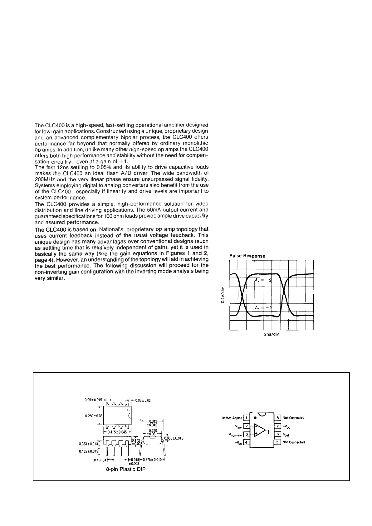
Package Dimensions
Pinout
DIP & SOIC
© 1999 National Semiconductor Corporation http://www.national.com
Printed in the U.S.A.
The CLC400 is available in several versions to meet a variety of requirements. A three-letter suffix determines the version:
CLC400AJP -40°C to +85°C 8-pin plastic DIP
CLC400AJE -40°C to +85°C 8-pin plastic SOIC
CLC400AIB -40°C to +85°C 8-pin hermetic CERDIP
CLC400A8B -55°C to +125°C 8-pin hermetic CERDIP,
MIL-STD-833, Level B
DESC SMD number: 5962-89970

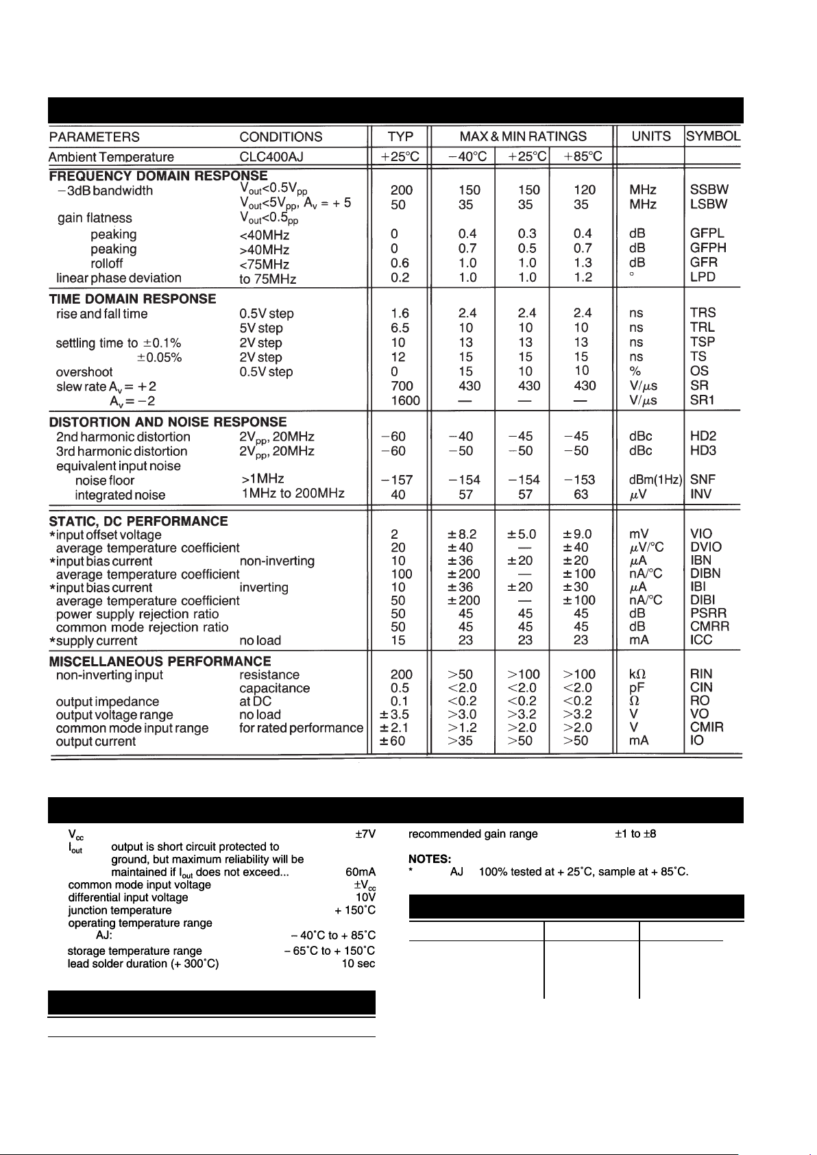
CLC400 Electrical Characteristics
(Av= +2,Vcc= ±5V, RL= 100Ω,Rf= 250Ω; unless specified)
Absolute Maximum Ratings Miscellaneous Ratings
http://www.national.com 2
Min/max ratings are based on product characterization and simulation. Individual parameters are tested as noted. Outgoing quality levels are
determined from tested parameters.
EDS rating (human body model) 500V
Pac kage Thermal Resistance
Package θ
JC
θ
JA
AJP 70°C/W 125°C/W
AJE 65°C/W 145°C/W
AIB 35°C/W 145°C/W
A8B 35°C/W 145°C/W
Reliability Information
Transistor count 24
 Loading...