NSC CLC231AK, CLC231AI, CLC231A8CC, CLC231A8AC Datasheet

Features
■
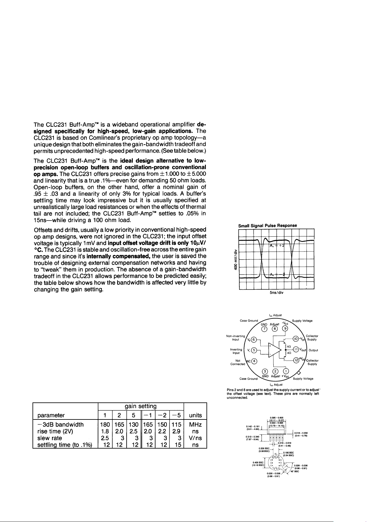
165MHz closed-loop – -3dB bandwidth
■
15ns settling to 0.05%
■
1mV input offset voltage, 10µV/°C drift
■
100mA output current
■
Excellent AC and DC linearity
Applications
■
Driving flash A/D converters
■
Precision line driving
(a gain of 2 cancels matched-line losses)
■
DAC current-to-voltage conversion
■
Low-power, high-speed applications
(50mW @ ±5V)
General Description
Comlinear CLC231
Fast Settling, Wideband Buff-Amp™ (A
v = ±1 to ±5)
N
August 1996
Comlinear CLC231
Fast Settling, Wideband Buff-Amp™ (A
v
= ±1 to ±5)
Typical Performance
Package Dimensions
Bottom View
The CLC231 is constructed using thin film resistor/bipolar transistor technology, and is available in the following versions:
CLC231AI -25°C to +85°C 12-pin TO-8 can
CLC231A8C -55°C to +125°C 12-pin TO-8 can,
MIL-STD-883, Level B
CLC231AK -55°C to +125°C 12-pin TO-8 can, features burn-in
and hermetic testing
CLC231AM -55°C to +125°C 12-pin TO-8 can, screened to
Comlinear’s M standard for high
reliability
DESC SMD number: 5962-89594
© 1996 National Semiconductor Corporation http://www.national.com
Printed in the U.S.A.
Not Intended For New Designs

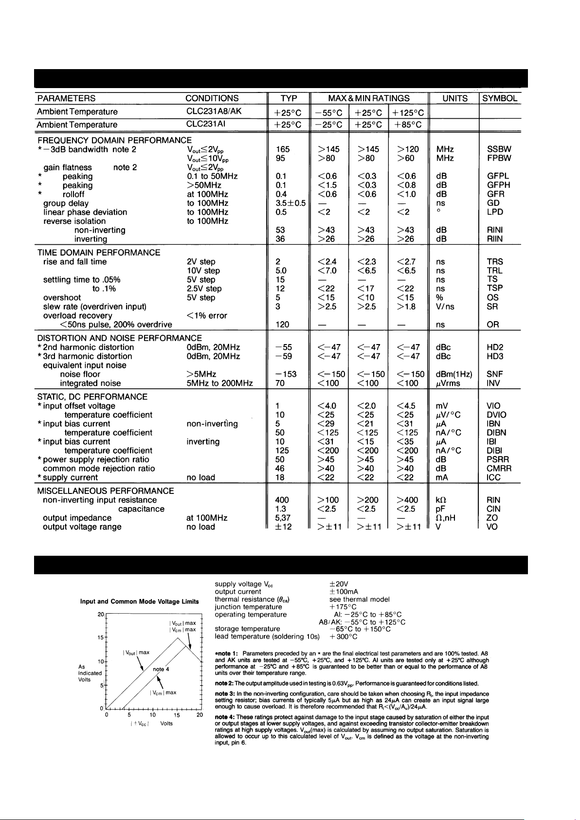
CLC231 Electrical Characteristics
(Av= +2, Vcc= ±15V, RL= 100Ω, Rf= 250Ω; unless specified)
Absolute Maximum Ratings
http://www.national.com 2
Min/max ratings are based on product characterization and simulation. Individual parameters are tested as noted. Outgoing quality levels are
determined from tested parameters.
 Loading...