NSC CLC200AI, CLC200A8CC, CLC200A8AC Datasheet

Features
■
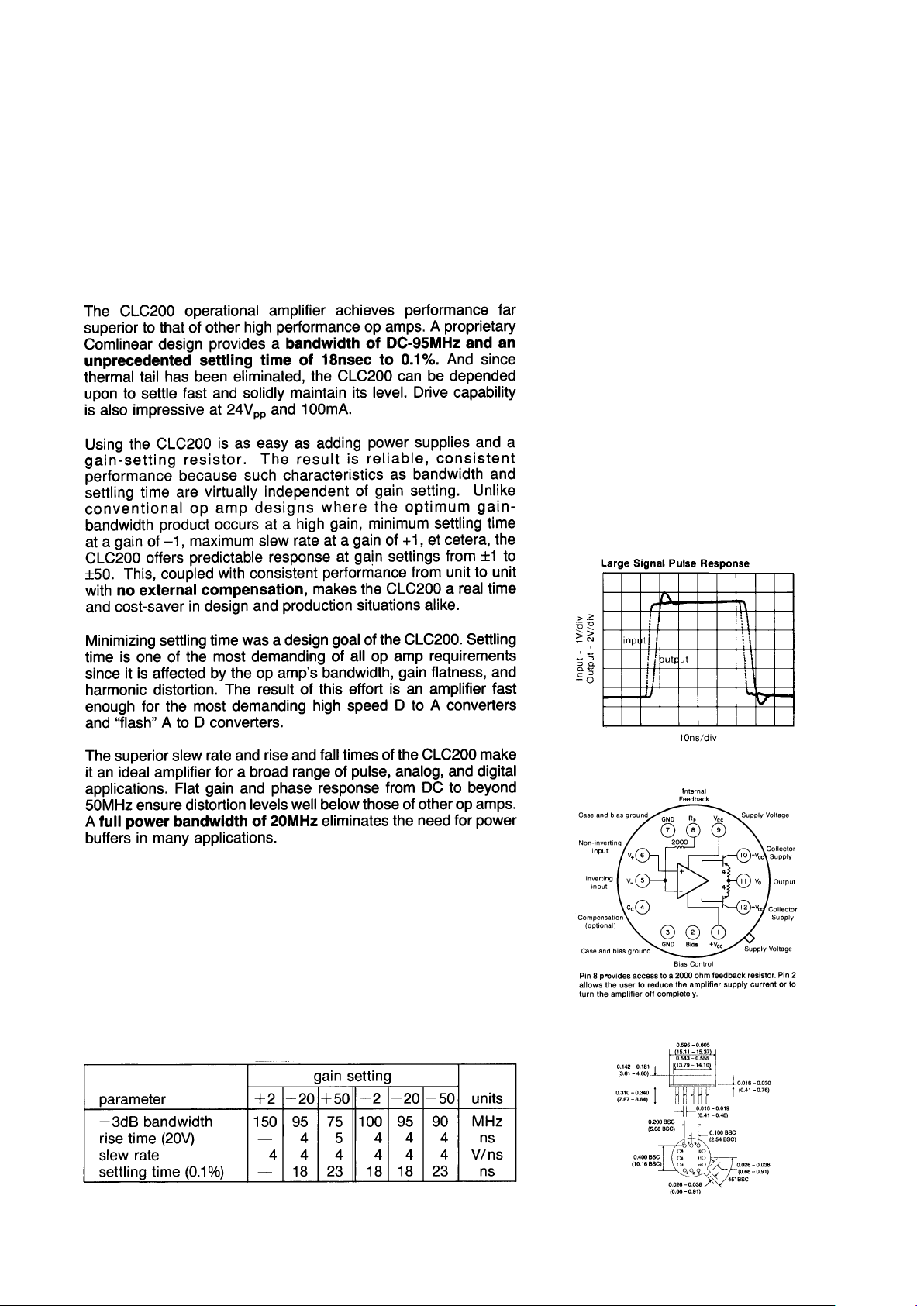
-3dB bandwidth of 95MHz
■
0.1% settling in 18ns
■
4000V/µs slew rate
■
Low distortion, linear phase
■
3.6ns rise and fall times
Applications
■
Fast, precision Ato D, D to Aconversion
■
Baseband and video communications
■
Radar, sonar, IF processors
■
Laser drivers, photodiode preamps
■
High-density buffering
■
Graphic CRT composite video drive amp
General Description
Comlinear CLC200
Fast Settling, Wideband Operational Amplifiers
N
August 1996
Comlinear CLC200
Fast Settling, Wideband Operational Amplifiers
Typical Performance
Package Dimensions
Bottom View
The CLC200 is constructed using thin film resistor/bipolar transistor technology, and is available in the following versions:
CLC200AI -25°C to +85°C 12-pin TO-8 can
CLC200A8C -55°C to +125°C 12-pin TO-8 can,
MIL-STD-883, Level B
CLC200AK -55°C to +125°C 12-pin TO-8 can, features burn-in
and hermetic testing
CLC200AM -55°C to +125°C 12-pin TO-8 can, screened to
Comlinear’s M std. for high reliability
DESC SMD number: 5962-89910
© 1996 National Semiconductor Corporation http://www.national.com
Printed in the U.S.A.
Not Intended For New Designs

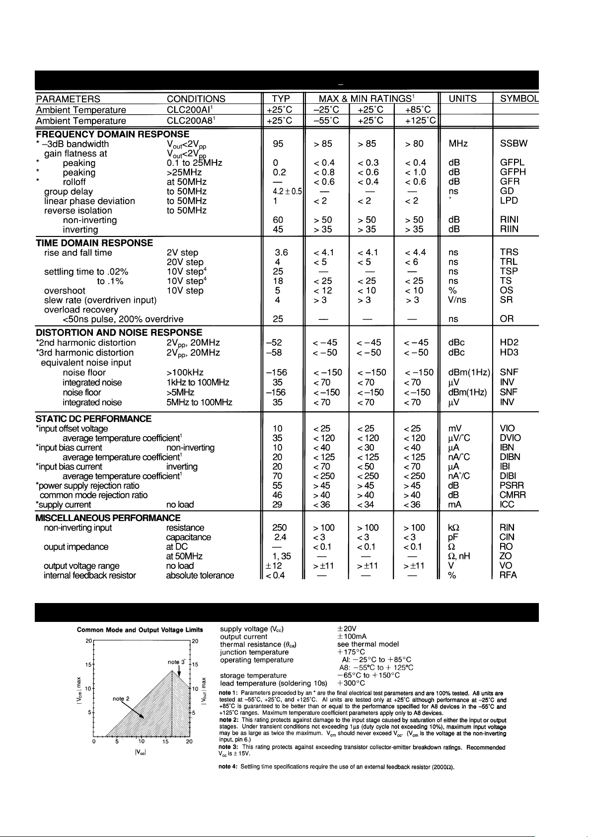
CLC200 Electrical Characteristics
(Av= +20,Vcc= +5V, RL= 200Ω, Rf= 2000Ω; unless specified)
Absolute Maximum Ratings
http://www.national.com 2
Min/max ratings are based on product characterization and simulation. Individual parameters are tested as noted. Outgoing quality levels are
determined from tested parameters.
 Loading...