NSC CLC114AJE, CLC114AJ-MLS, CLC114AJP, CLC114AJE-TR13, 5962-9233901M2A Datasheet

Features
■
Closed-loop, quad buffer
■
200MHz small-signal bandwidth
■
450V/µs slew rate
■
Low power, 30mW per channel (±5V sup.)
■
62dB channel isolation (10MHz)
■
Specified for crosspoint switch loads
Applications
■
Video crosspoint switch driver
■
Video distribution buffers
■
Video switching buffers
■
Video signaling multiplexing
■
Instrumentation amps
■
Active filters
General Description
CLC114
Quad, Low-P ower Video Buffer
N
June 1999
CLC114
Quad, Lo w-Po wer Video Buffer
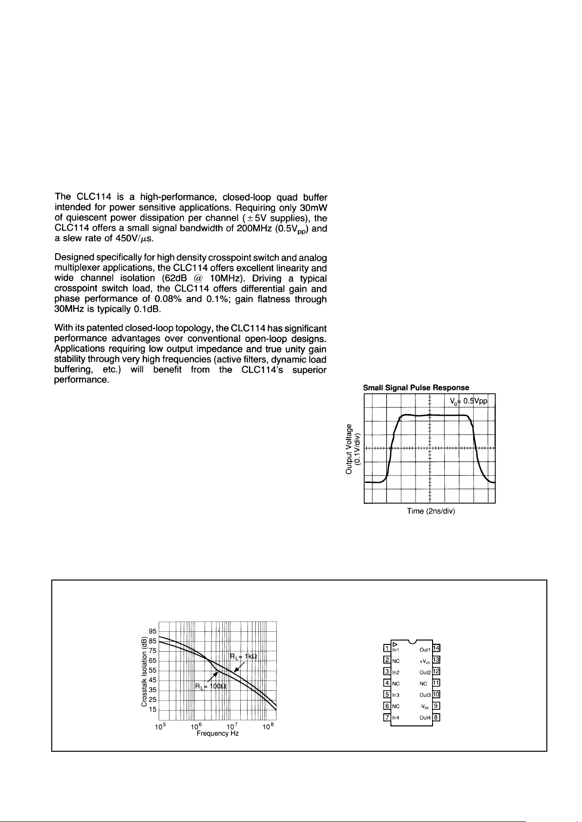
Pinout
Typical Application
© 1999 National Semiconductor Corporation http://www.national.com
Printed in the U.S.A.
Constructed using an advancd, complementary bipolar process and
National’s proven high-speed architectures, the CLC114 is available
in several versions to meet a variety of requirements.
CLC114AJP -40°C to +85°C 14-pin plastic DIP
CLC114AJE -40°C to +85°C 14-pin plastic SOIC
CLC114ALC -40°C to +85°C dice
CLC114AMC -55°C to +125°C dice qualified to Method 5008,
MIL-STD-883, Level B
CLC114A8B -55°C to +125°C 14-pin CERDIP,
MIL-STD-883, Level B
DESC SMD number: 5962-92339

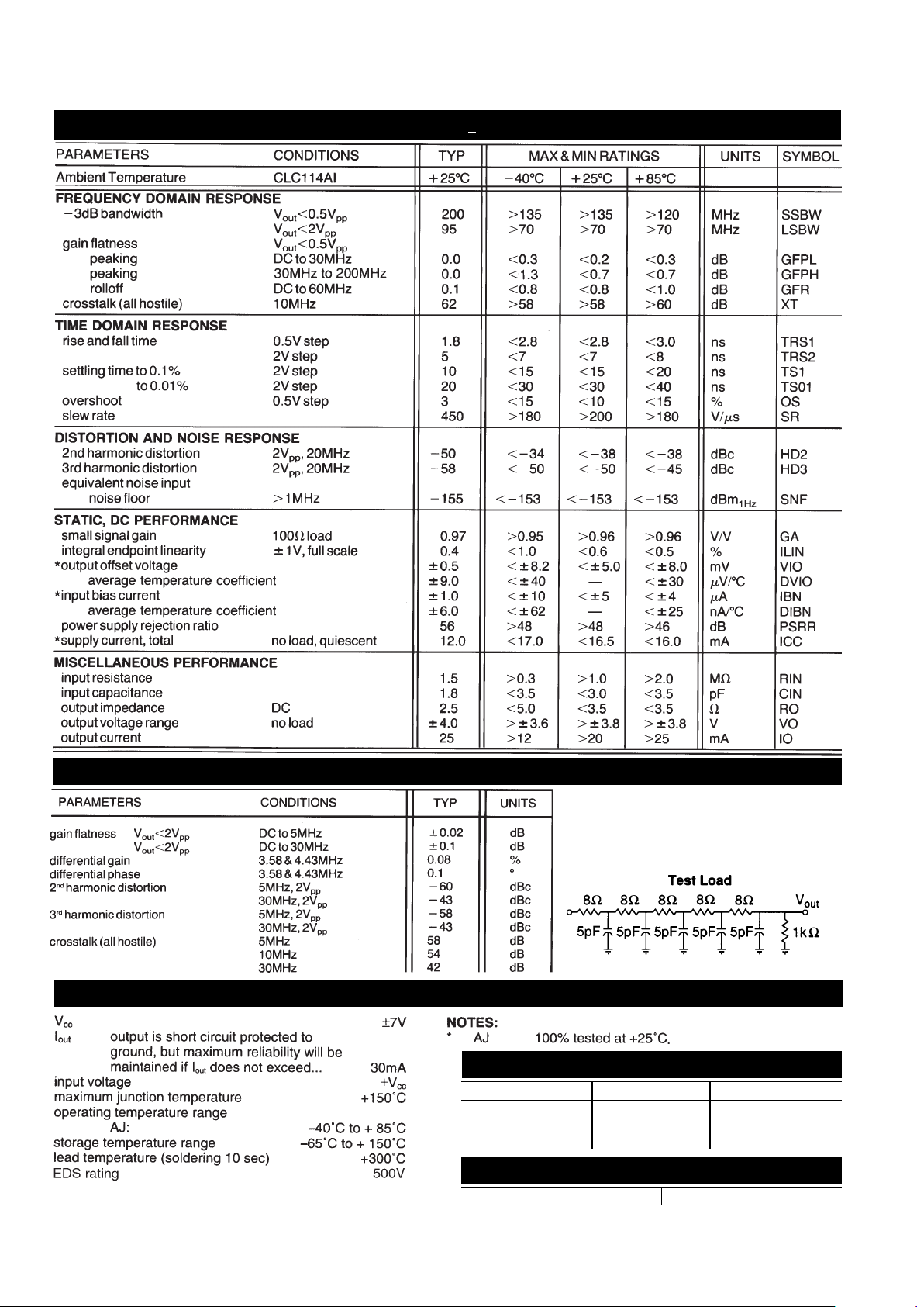
CLC114 Electrical Characteristics
(Vcc= +5V, RL= 100Ω unless specified)
Performance Driving a Crosspoint Swtich
Absolute Maximum Ratings Miscellaneous Ratings
http://www.national.com 2
Min/max ratings are based on product
characterization and simulation. Individual
parameters are tested as noted. Outgoing
quality levels are determined from tested
parameters.
Reliability Information
Transistor Count 64
Pac kage Thermal Resistance
Package
θθ
JC
θθ
JA
Plastic (AJP) 65°C/W 115°C/W
Surface Mount (AJE) 55°C/W 125°C/W
CERDIP 35°C/W 90°C/W
 Loading...