Features
■
Closed-loop, unity-gain operation
■
-3dB bandwidths of 730MHz (0.5Vpp)
■
0.2% settling in 5ns
■
Low power, 150mW
■
Low distortion, -65dBc at 20MHz
Applications
■
Ultra-fast flash A/D conversion
■
Line driving
■
High-speed communications
■
Impedance transformation
■
Power buffers
■
IF processors
General Description
CLC110
Wideband, Closed-Loop Monolithic Buffer Amplifier
N
June 1999
CLC110
Wideband, Closed-Loop Monolithic Buffer Amplifier
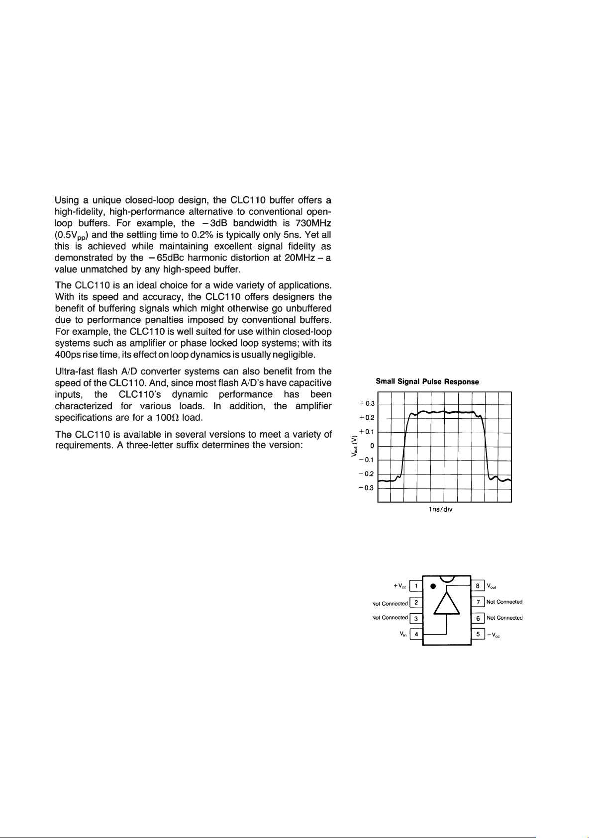
Pinout
DIP & SOIC
© 1999 National Semiconductor Corporation http://www.national.com
Printed in the U.S.A.
CLC110AJP -40°C to +85°C 8-pin plastic DIP
CLC110AJE -40°C to +85°C 8-pin plastic SOIC
DESC SMD number: 5962-89975

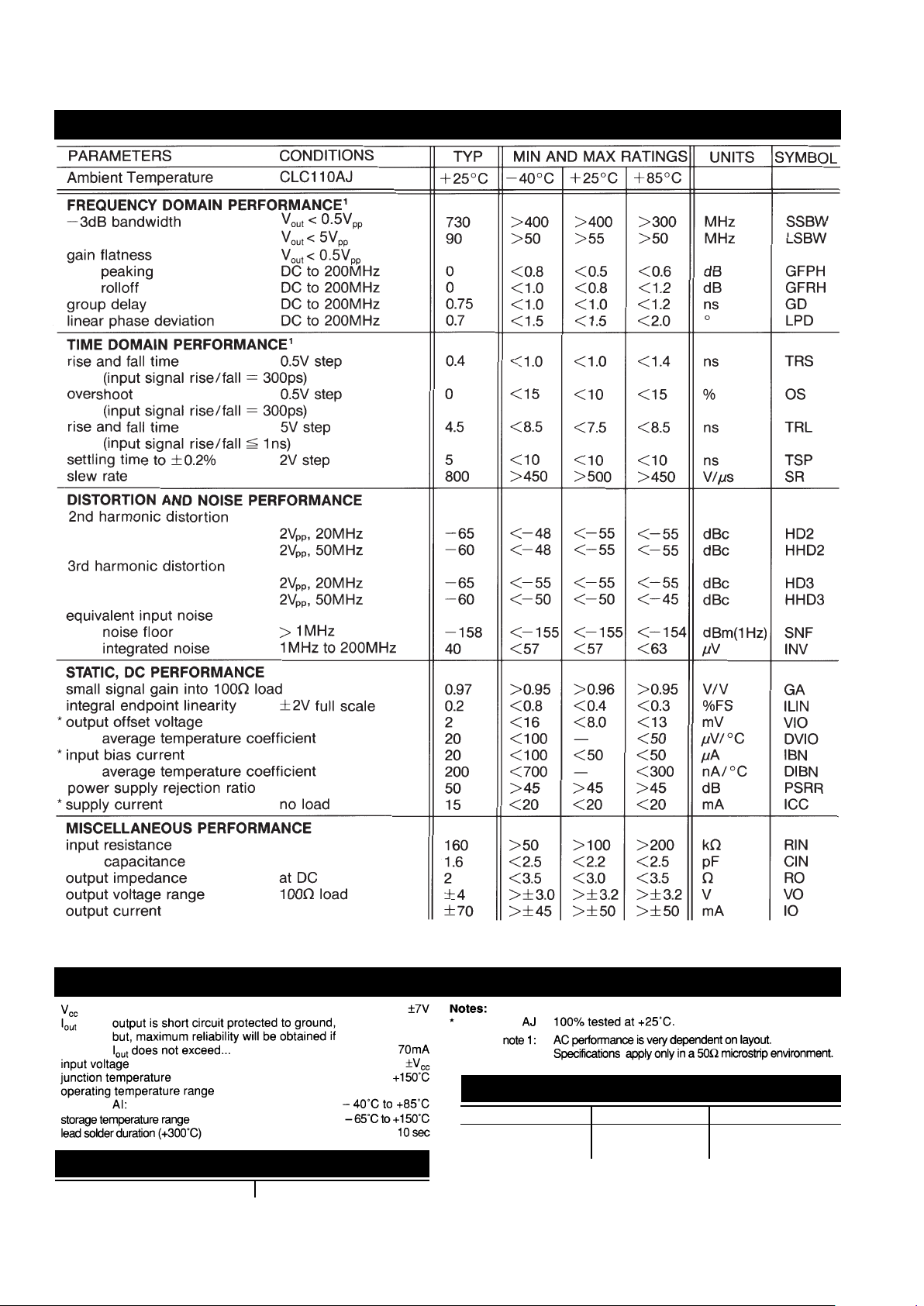
CLC110 Electrical Characteristics
(Vcc= ±5V, RL= 100Ω,Rs= 50Ω; unless specified)
Absolute Maximum Ratings Miscellaneous Ratings
http://www.national.com 2
Min/max ratings are based on product characterization and simulation. Individual parameters are tested as noted. Outgoing quality levels are
determined from tested parameters.
Reliability Information
Transistor Count 21
Pac kage Thermal Resistance
Package
θθ
JC
θθ
JA
Plastic (AJP) 65°C/W 115°C/W
Surface Mount (AJE) 55°C/W 125°C/W
 Loading...