

NSC CLC030VEC Datasheet
PRELIMINARY
February 2002
CLC030
SMPTE 292M/259M Digital Video Serializer with Video
and Ancilliary Data FIFOs and Integrated Cable Driver
General Description
The CLC030 SMPTE 292M/259M Digital Video Serializer
with Ancilliary Data FIFO and Integrated Cable Driver is a
monolithic integrated circuit that encodes, serializes and
transmits bit-parallel digital video data conforming to SMPTE
125M and 267M standard definition, 10-bit wide component
video and SMPTE 260M, 274M, 295M and 296M highdefinition, 20-bit wide component video standards. The
CLC030 operates at SMPTE 259M serial data rates of
270 Mbps, 360 Mbps, the SMPTE 344M (proposed) serial
data rate of 540 Mbps; and the SMPTE 292M serial data
rates of 1483.5 and 1.485 Gbps. The serial data clock frequency is internally generated and requires no external frequency setting, trimming or filtering components*.
Functions performed by the CLC030 include: parallel-toserial data conversion, SMPTE standard data encoding,
NRZ to NRZI data format conversion, serial data clock generation and encoding with the serial data, automatic video
rate and format detection, ancilliary data packet storage,
manipulation and insertion, and serial data output driving.
The CLC030 has circuitry for automatic EDH/CRC character
and flag generation and insertion per SMPTE RP-165 (standard definition) or SMPTE 292M (high definition). Optional
LSB dithering is implemented which prevents pathological
pattern generation. Unique to the CLC030 are its video and
ancilliary data FIFOs. The video FIFO allows from 0 to 4
parallel data clock delays to be inserted in the data path for
video timing purposes. The ancilliary data port and on-chip
FIFO and control circuitry offer elegant handling and insertion of ancilliary datapacketsandchecksumsin the ancilliary
data space. The CLC030 also has an exclusive built-in selftest (BIST) and video test pattern generator (TPG) with SD
and HD component video test patterns: reference black, PLL
and EQ pathologicals and colour bars in 4:3 and 16:9 raster
formats for NTSC and PAL standards*. The colour bar patterns feature optional bandwidth limiting coding in the
chroma and luma transitions.
The CLC030 has a unique multi-function I/O port which
provides access to control and configuration signals and
data. This port may be programmed to provide external
access to control functions and data for use as inputs and
outputs. This allows the designer greater flexibility in tailoring
the CLC030 to the desired application. At power-up or after a
reset command, the CLC030 is auto-configured to a default
operating condition. Separate power pins for the output
driver, PLL and the serializer improve power supply rejection, output jitter and noise performance.
The CLC030’s internal circuitry is powered from +2.5V and
the I/O circuitry from a +3.3V supply. Power dissipation is
typically 430mW at 1.485Gbps including two 75Ω ACcoupled and back-matched output loads. The device is packaged in a 64-pin TQFP.
Features
n SDTV/HDTV serial digital video standard compliant
n Supports 270 Mbps, 360 Mbps, 540 Mbps, 1.4835Gbps
and 1.485 Gbps SDV data rates with auto-detection
n LSB dithering option
n No external serial data rate setting or VCO filtering
components required*
n Fast PLL lock time:
n Adjustable depth video FIFO for timing alignment
n Built-in self-test (BIST) and video test pattern generator
(TPG)*
n Automatic EDH/CRC word and flag generation and
insertion
n On-chip ancilliary data FIFO and insertion control
circuitry
n Flexible control and configuration I/O port
n LVCMOS compatible data and control inputs and
outputs
n 75Ω ECL-compatible, differential, serial cable-driver
outputs
n 3.3V I/O power supply, 2.5V logic power supply
operation
n Low power: typically 430mW
n 64-pin TQFP package
n Commercial temperature range 0˚C to +70˚C
*
Patent applications made or pending.
<
150µs typical at 1.485 Gbps
Applications
n SDTV/HDTV parallel-to-serial digital video interfaces for:
— Video cameras
— VTRs
— Telecines
— Digital video routers and switchers
— Digital video processing and editing equipment
— Video test pattern generators and digital video test
equipment
— Video signal generators
CLC030 SMPTE 292M/259M Digital Video Serializer with Video and Ancilliary Data FIFOs and
Integrated Cable Driver
Order Number CLC030VEC 64-Pin TQFP
© 2002 National Semiconductor Corporation DS200003 www.national.com
NS Package Number
VEC-64A
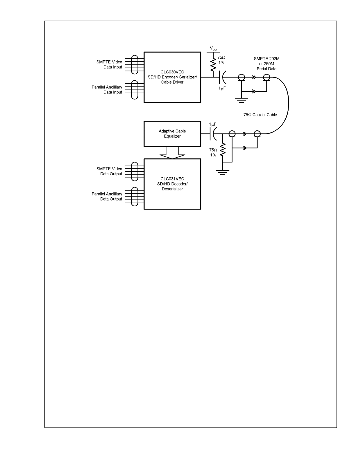
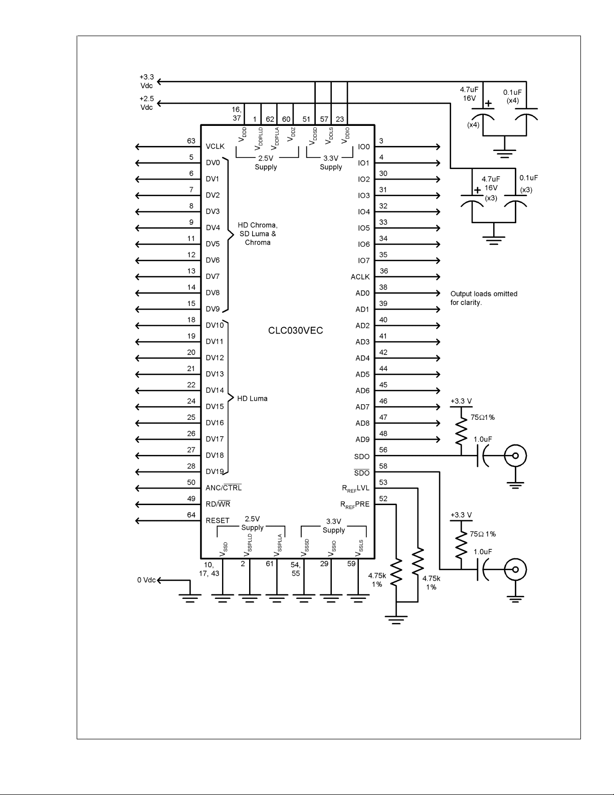
Typical Application
CLC030
DS200003-1
www.national.com 2
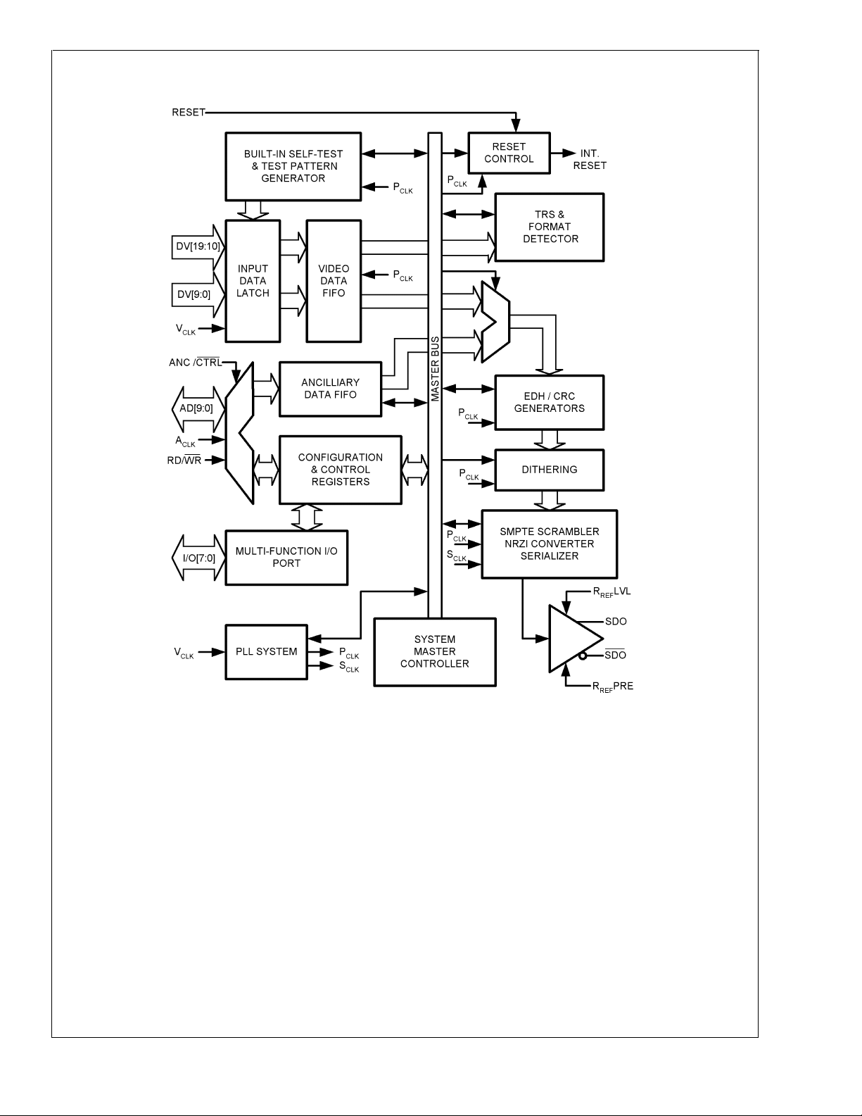
Block Diagram
CLC030
DS200003-2
www.national.com3
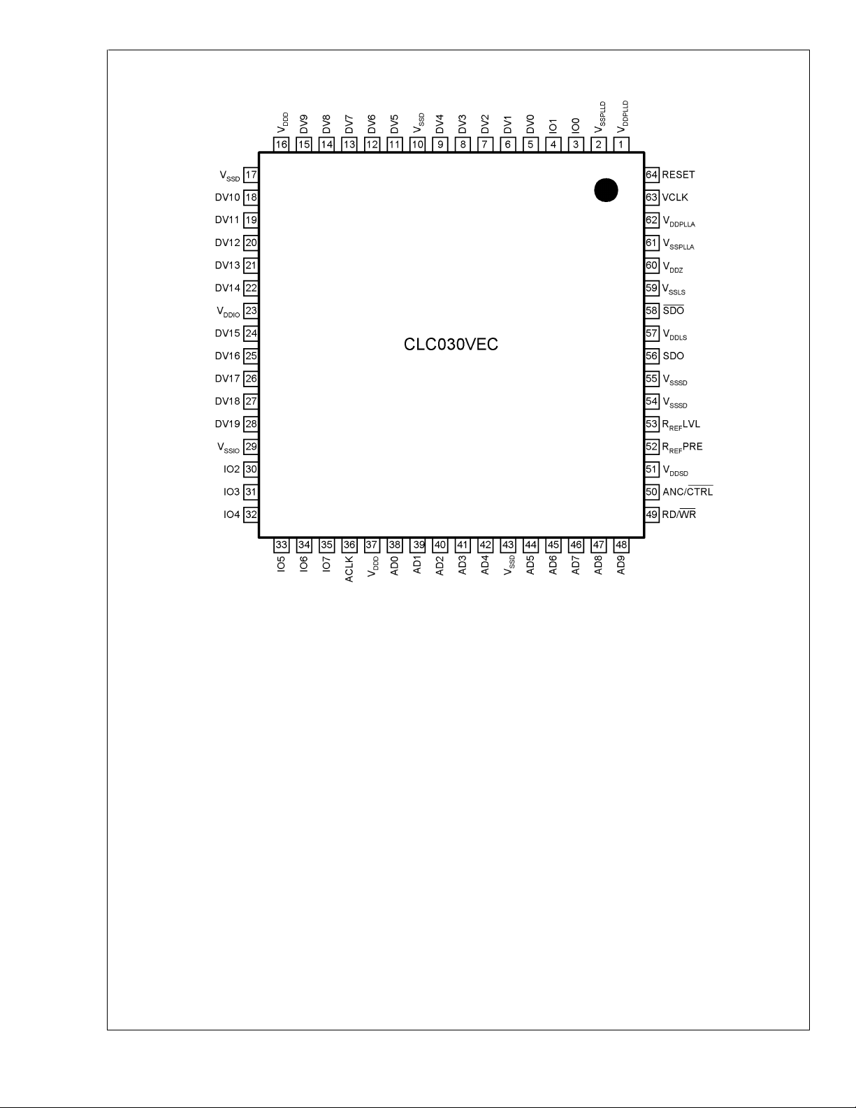
Connection Diagram
CLC030
64-Pin TQFP
Order Number CLC030VEC
See NS Package Number VEC-64A
DS200003-3
www.national.com 4
CLC030
Absolute Maximum Ratings (Note 1)
It is anticipated that this device will not be offered in
a military qualified version. If Military/Aerospace speci-
fied devices are required, please contact the National
Semiconductor Sales Office / Distributors for availability
and specifications.
CMOS Input Current (single input):
Vi=V
Vi=V
CMOS Output Source/Sink Current:
−0.15V: −5 mA
SSIO
+0.15V: +5 mA
DDIO
±
10 mA
SDO Output Sink Current: 40 mA
Package Thermal Resistance
CMOS I/O Supply Voltage
(V
DDIO–VSSIO
): 4.0V
SDO Supply Voltage
(V
DDSD–VSSSD
): 4.0V
Digital Logic Supply Voltage
(V
DDD–VSSD
): 3.0V
PLL Supply Voltage
(V
DDPLL–VSSPLL
): 3.0V
CMOS Input Voltage
(Vi):
CMOS Output Voltage
(Vo):
V
V
SSIO
V
SSIO
V
DDIO
DDIO
−0.15V to
+0.15V
−0.15V to
+0.15V
@
0 LFM Airflow 47˚C/W
θ
JA
@
500 LFM Airflow 27˚C/W
θ
JA
θ
JC
6.5˚C/W
Storage Temp. Range: −65˚C to +150˚C
Junction Temperature: +150˚C
Lead Temperature (Soldering 4 Sec): +260˚C
ESD Rating (HBM): 2 kV
ESD Rating (MM): 250V
Recommended Operating Conditions
Symbol Parameter Conditions Reference Min Typ Max Units
V
V
V
V
V
V
T
t
JIT
DDIO
DDSD
DDD
DDPLL
IL
IH
A
CMOS I/O Supply
V
DDIO−VSSIO
Voltage
SDO Supply Voltage V
Digital Logic Supply
DDSD−VSSSD
V
DDD–VSSD
Voltage
PLL Supply Voltage V
DDPLL–VSSPLL
CMOS Input Voltage,
Low Level
CMOS Input Voltage
High Level
Operating Free Air
Temperature
Video Clock Jitter V
CLK
3.150 3.300 3.450 V
3.150 3.300 3.450 V
2.375 2.500 2.625 V
2.375 2.500 2.625 V
V
SSIO
V
DDIO
0 +70 ˚C
100 ps
V
V
P-P
DC Electrical Characteristics
Over Supply Voltage and Operating Temperature ranges, unless otherwise specified (Notes 2, 3).
Symbol Parameter Conditions Reference Min Typ Max Units
V
IH
V
IL
I
IH
I
IL
V
OH
V
OL
V
SDO
I
DD
(3.3V)
I
DD
(3.3V)
Input Voltage High Level All LVCMOS
Input Voltage Low Level V
Input Current High Level VIH=V
Input Current Low Level VIL=V
CMOS Output Voltage
DDIO
SSIO
IOH= −6.6 mA All LVCMOS
High Level
CMOS Output Voltage
IOL= +6.6 mA
Inputs
Outputs
Low Level
Serial Driver Output
Voltage
Power Supply Current,
3.3V Supply, Total
Test Circuit, Test Loads
Shall Apply
V
= 27 MHz, NTSC
CLK
Colour Bar Pattern, Test
SDO, SDO
V
DDIO,VDDSD
Circuit, Test Loads Shall
Apply
Power Supply Current,
3.3V Supply, Total
V
= 74.25 MHz, NTSC
CLK
Colour Bar Pattern, Test
V
DDIO,VDDSD
Circuit, Test Loads Shall
Apply
2.0 V
SSIO
DDIO
0.8 V
+90 +150 µA
−1 −20 µA
2.4 2.7 V
V
V
SSIO
SSIO
+0.3
DDIO
V
SSIO
+0.5V
720 800 880 mV
48 65 mA
66 90 mA
www.national.com5
V
V
V
P-P
DC Electrical Characteristics (Continued)
Over Supply Voltage and Operating Temperature ranges, unless otherwise specified (Notes 2, 3).
CLC030
Symbol Parameter Conditions Reference Min Typ Max Units
I
DD
(2.5V)
Power Supply Current,
2.5V Supply, Total
V
= 27 MHz, NTSC
CLK
Colour Bar Pattern, Test
Circuit, Test Loads Shall
V
DDD,VDDZ
V
DDPLL
,
66 85 mA
Apply
I
DD
(2.5V)
Power Supply Current,
2.5V Supply, Total
V
= 74.25 MHz, NTSC
CLK
Colour Bar Pattern, Test
Circuit, Test Loads Shall
V
DDD,VDDZ
V
DDPLL
,
85 110 mA
Apply
AC Electrical Characteristics
Over Supply Voltage and Operating Temperature ranges, unless otherwise specified (Note 3).
Symbol Parameter Conditions Reference Min Typ Max Units
f
VCLK
DC
V
f
ACLK
DC
A
t
r,tf
BR
SDO
tr,t
f
t
r,tf
t
j
t
j
t
LOCK
t
LOCK
t
S
t
H
t
S
t
H
Note 1: “Absolute Maximum Ratings” are those parameter values beyond which the life and operation of the device cannot be guaranteed. The stating herein of
these maximums shall not be construed to imply that the device can or should be operated at or beyond these values. The table of “Electrical Characteristics”
specifies acceptable device operating conditions.
Note 2: Current flow into device pins is defined as positive. Current flow out of device pins is defined as negative. All voltages are referenced to V
Note 3: Typical values are stated for V
Note 4: Spec. is guaranteed by design.
Note 5: R
Note 6: R
Note 7: Measured from rising-edge of first DV
Note 8: Average value measured between rising edges computed over at least one video field.
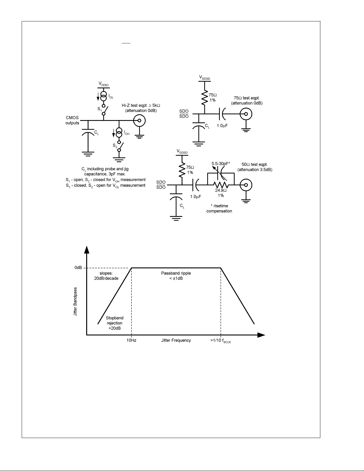
Note 9: Intrinsic timing jitter is measured in accordance with SMPTE RP 184-1996, SMPTE RP 192-1996 and the applicable serial data transmission standard,
SMPTE 259M-1997 or SMPTE 292M (proposed). A colour bar test pattern is used. The value of f
344M or 1,485 MHz for SMPTE 292M serial data rates. See Timing Jitter Bandpass section.
Parallel Video Clock
Frequency
Video Clock Duty
Cycle
Ancilliary Clock
Frequency
Ancilliary Clock Duty
Cycle
Input Clock and Data
Rise Time, Fall Time
10%–90% V
V
CLK
V
CLK
A
CLK
A
CLK
CLK,ACLK
,AD
DV
N
27 74.25 MHz
45 50 55 %
V
CLK
45 50 55 %
,
N
1.0 1.5 3.0 ns
Serial Data Rate (Notes 5, 6) SDO, SDO 270 1,485 M
Rise Time, Fall Time 20%–80%, (Note 6) SDO, SDO 270 ps
Rise Time, Fall Time 20%–80%, (Note 5) SDO, SDO 500 ps
Output Overshoot (Note 4) SDO, SDO
Serial Output Jitter,
270 M
, (Notes 5, 9, 10) SDO, SDO
bps
Intrinsic
Serial Output Jitter,
1,485 M
, (Notes 6, 9, 10) SDO, SDO
bps
Intrinsic
5%
200 ps
120 ps
Lock Time (Notes 5, 7) (SD Rates) 15 ms
Lock Time (Notes 6, 7) (HD Rates) 15 ms
Setup Time, Video
Data
Hold Time, Video
Data
Setup Time, Anc.
Data Port
Hold Time, Anc. Data
Port
=75Ω, AC-coupled@270 M
L
=75Ω, AC-coupled@1,485 M
L
Timing Diagram, (Note 4) DVNto V
Timing Diagram, (Note 4) V
Timing Diagram, (Note 4) ADNto A
Timing Diagram, (Note 4) A
DDIO=VDDSD
LVL = R
bps,RREF
bps,RREF
cycle until Lock Detect output goes high (true). Lock time includes format detection time plus PLL lock time.
CLK
= +3.3V, V
LVL = R
DDD=VDDPLL
PRE = 4.75 kΩ 1%, See Test Loads and Test Circuit.
REF
PRE = 4.75 kΩ 1%, See Test Loads and Test Circuit.
REF
= +2.5V and TA= +25˚C.
CLK
to DV
CLK
CLK
SCLK
N
CLK
to AD
N
is 270 MHz or 360 MHz for SMPTE 259M, 540MHz for SMPTE
1.5 2.0 ns
1.5 2.0 ns
1.5 2.0 ns
1.5 2.0 ns
SS
MHz
bps
P-P
P-P
=0V.
www.national.com 6
AC Electrical Characteristics (Continued)
Note 10: Intrinsic jitter is defined in accordance with SMPTE RP 184-1996 as: jitter at an equipment output in the absence of input jitter. As applied to this device,
the input port is V
and the output port is SDO or SDO.
CLK
Test Loads
CLC030
Timing Jitter Bandpass
DS200003-4
DS200003-6
www.national.com7
Test Circuit
CLC030
www.national.com 8
DS200003-7
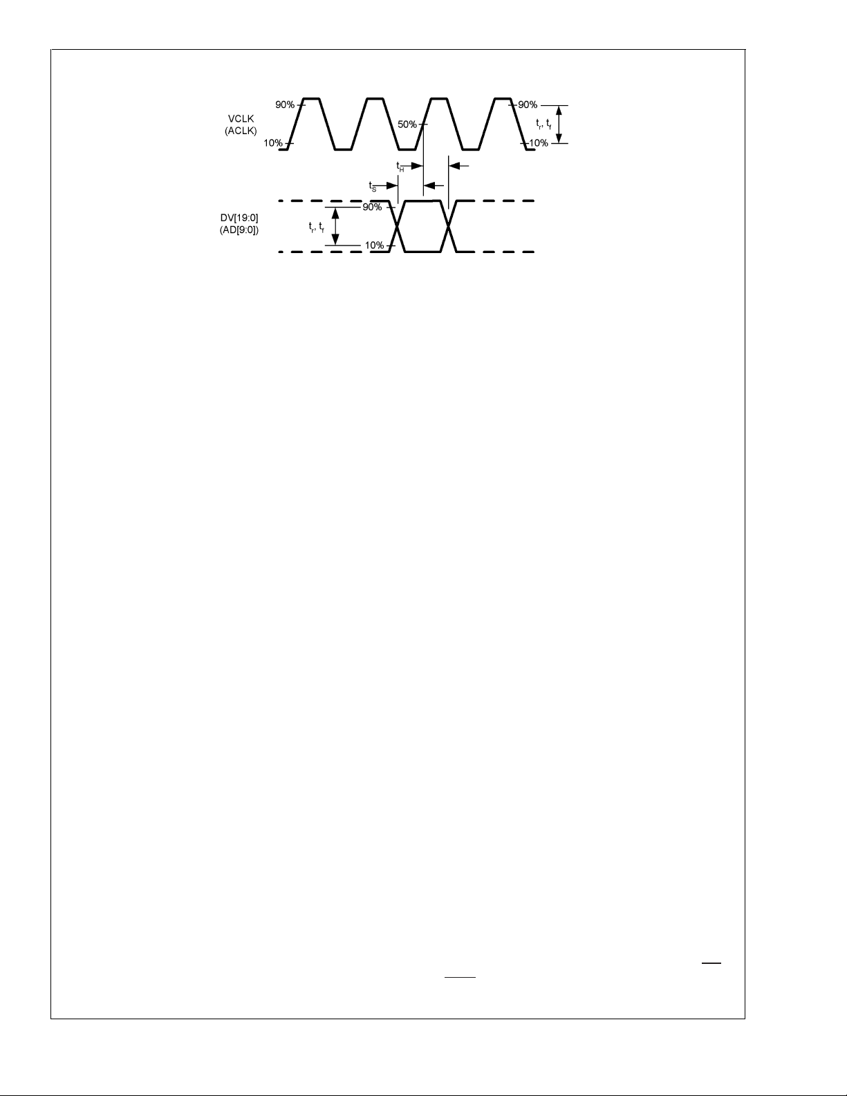
Timing Diagram
Device Operation
The CLC030 SDTV/HDTV Serializer is used in digital video
signal origination equipment: cameras, video tape recorders,
telecines and video test and other equipment. It converts
parallel SDTV or HDTV component digital video signals into
serial format. Logic levels within this equipment are normally
produced by LVCMOS logic devices. The encoder produces
serial digital video (SDV) signals conforming to SMPTE
259M, SMPTE 344M (proposed) or SMPTE 292M. The
CLC030 operates at parallel data rates of 27.0 MHz, 36.0
MHz, 54.0 MHz, 74.176MHz and 74.25 MHz. Corresponding
serial data rates are 270 Mbps, 360 Mbps, 540 Mbps,
1.4835Gbps and 1.485 Gbps. Segmented frame formats are
not supported.
VIDEO DATA PATH
The input data register accepts 10-bit standard definition or
20-bit high definition parallel data and associated clock signals having LVCMOS-compatible signal levels. All parallel
video data inputs, DV[19:0], have internal pull-down devices. VCLK does not have an internal pull-down device.
Parallel video data may conform to any of several SMPTE
standards: 125M, 267M, 260M, 274M, 295M or 296M. Segmented frame formats are not supported. For HDTV data,
the upper 10 bits of the DV input are luminance (luma)
information and the lower 10 bits are colour difference
(chrominance or chroma) information. For SDTV data, the
lower order 10 bits contain both luma and chroma information. Output from this register feeds the video FIFO, video
format detection circuit, TRS character detector, SMPTE
scrambler, EDH/CRC generators, serializer/NRZI converter
and the device control system.
Data from the input data register passes into a 4-register
deep video FIFO prior to encoding and other processing.
The depth of this FIFO is set by a word written into the
VIDEO FIFO Depth[2:0] bits in the ANC 0 control register.
The video format detector automatically determines the
raster characteristics (video data format) of the parallel input
data and configures the CLC030 to properly handle the data.
This assures that the data will be properly formatted, that the
correct data rate is selected and that ancilliary data, line
numbers (HD) and CRC/EDH data are correctly inserted.
Indication of the standard being processed is stored in the
FORMAT[4:0] bits in the FORMAT 1 control data register.
This format data can be programmed for output on the
multi-function I/O port.
The CLC030 may be configured to operate at a single video
format by writing the appropriate FORMAT SET[4:0] control
data into the FORMAT 0 control register. Also, the CLC030
may be configured to handle only the standard-definition
DS200003-8
data formats by setting the SD ONLY bit or only the highdefinition data formats by setting the HD ONLY bit in the
FORMAT 0 control register. When both of these bits are
reset the part automatically detects the data rate and range.
The TRS character detector processes the timing reference signals which control raster framing. The TRS detector
supplies control signals to the system controller to identify
the presence of the valid video data. The system controller
supplies necessary control signals to the EDH/CRC control
block. TRS character LSB-clipping as prescribed in ITU-R
BT.601 is used. LSB-clipping causes all TRS characters with
a value between 000h and 003h to be forced to 000h and all
TRS characters with a value between 3FCh and 3FFh to be
forced to 3FFh. Clipping is done prior to scrambling and
EDH/CRC character generation.
The CLC030 incorporates circuitry that implements the proposed SMPTE recommended practice and method for LSB
dithering. Control of this circuitry is via the Dither Enable bit
in the VIDEO INFO 0 control register. Dithering can be
selectively enabled during the vertical blanking interval by
use of the V Dither Enable bit in the VIDEO INFO 0 control
register. The initial condition of Dither Enable and V Dither
Enable is OFF.
The SMPTE scrambler accepts 10-bit standard definition or
20-bit high definition parallel video data and encodes it using
the polynomial X
standard in SMPTE 259M, SMPTE 344M (proposed) or
SMPTE 292M. The data is then serialized and sent to the
NRZ-to-NRZI converter before being output. The transmission bit order is LSB-first.
The NRZ-to-NRZI converter accepts NRZ serial data from
the SMPTE scrambler. The data is converted to NRZI format
using the polynomial (X + 1). The converter’s output goes to
the output cable driver amplifier.
ANCILLIARY/CONTROL DATA PATH
The Ancilliary and Control Data Port serves two functions
in the CLC030. It is used to selectively load ancilliary data
into the Ancilliary Data FIFO for insertion into the video data
stream. The utilization and flow of ancilliary data within the
device is managed by a system of control bits, masks and
IDs in the control data registers. This port also provides
read/write access to contents of the configuration and control registers. Configuration of the multi-function I/O Port is
also controlled by information stored in the control data
registers. Ancilliary and control data are input via the 10-bit
Ancilliary/Control Data Port, AD[9:0]. The signals RD/WR,
ANC/CTRL and ACLK control data flow through the port.
The operation and frequency of ACLK is completely inde-
9+X4
+ 1 as specified in the respective
CLC030
www.national.com9
 Loading...