NSC CLC018AJVJQ Datasheet
CLC018
8 x 8 Digital Crosspoint Switch, 1.4 Gbps
General Description
National’s Comlinear CLC018 is a fully differential 8x8 digital
crosspoint switch capable of operating at data rates exceeding 1.4 Gbps per channel. Its non-blocking architecture utilizes eight independent 8:1 multiplexers to allow each output
to be independently connected to any input and any input to
be connected to any or all outputs. Additionally, each output
can be individually disabled and set to a high-impedance
state. This TRI-STATE
larger switch array sizes.
Low channel-to-channel crosstalk allows the CLC018 to provide superior all-hostile jitter of 50ps
fidelity along with low power consumption of 850 mW make
the CLC018 ideal for digital video switching plus a variety of
data communication and telecommunication applications.
The fully differential signal path provides excellent noise immunity, and the I/Os support ECL and PECL logic levels. In
addition, the inputs may be driven single-ended or differentially and accept a wide range of common mode levels including the positive supply. Single +5V or −5V supplies or
dual +5V supplies are supported. Dual supply mode allows
the control signals to be referenced to the positive supply
(+5V) while the high-speed I/O remains ECL compatible.
The double row latch architecture utilized in the CLC018 allows switch reprogramming to occur in the background during operation.Activationofthenew configuration occurs with
a single “configure” pulse. Data integrity and jitter performance on unchanged outputs are maintained during reconfiguration. Two reset modes are provided. Broadcast reset
results in all outputs being connected to input port DI0.
TRI-STATE Reset results in all outputs being disabled.
®
feature allows flexible expansion to
. This excellent signal
PP
The CLC018 is fabricated on a high-performance BiCMOS
process and is available in a 64-lead plastic quad flat pack
(PQFP).
Features
n Fully differential signal path
n Non-Blocking
n Flexible expansion to larger array sizes with very low
power
n Single +5/−5V or dual
n TRI-STATE outputs
n Double row latch architecture
n 64-lead PQFP package
Applications
n Serial digital video routing (SMPTE 259M)
n Telecom/datacom switching
n ATM SONET
Key Specifications
n High speed:>1.4 Gbps
n Low jitter:
<
50 psPPfor rates<500 Mbps
<
100 psPPfor rates<1.4 Gbps
n Low power; 850 mW with all outputs active
n Fast output edge speeds: 250 ps
±
5V operation
CLC0188x8Digital Crosspoint Switch, 1.4 Gbps
October 1998
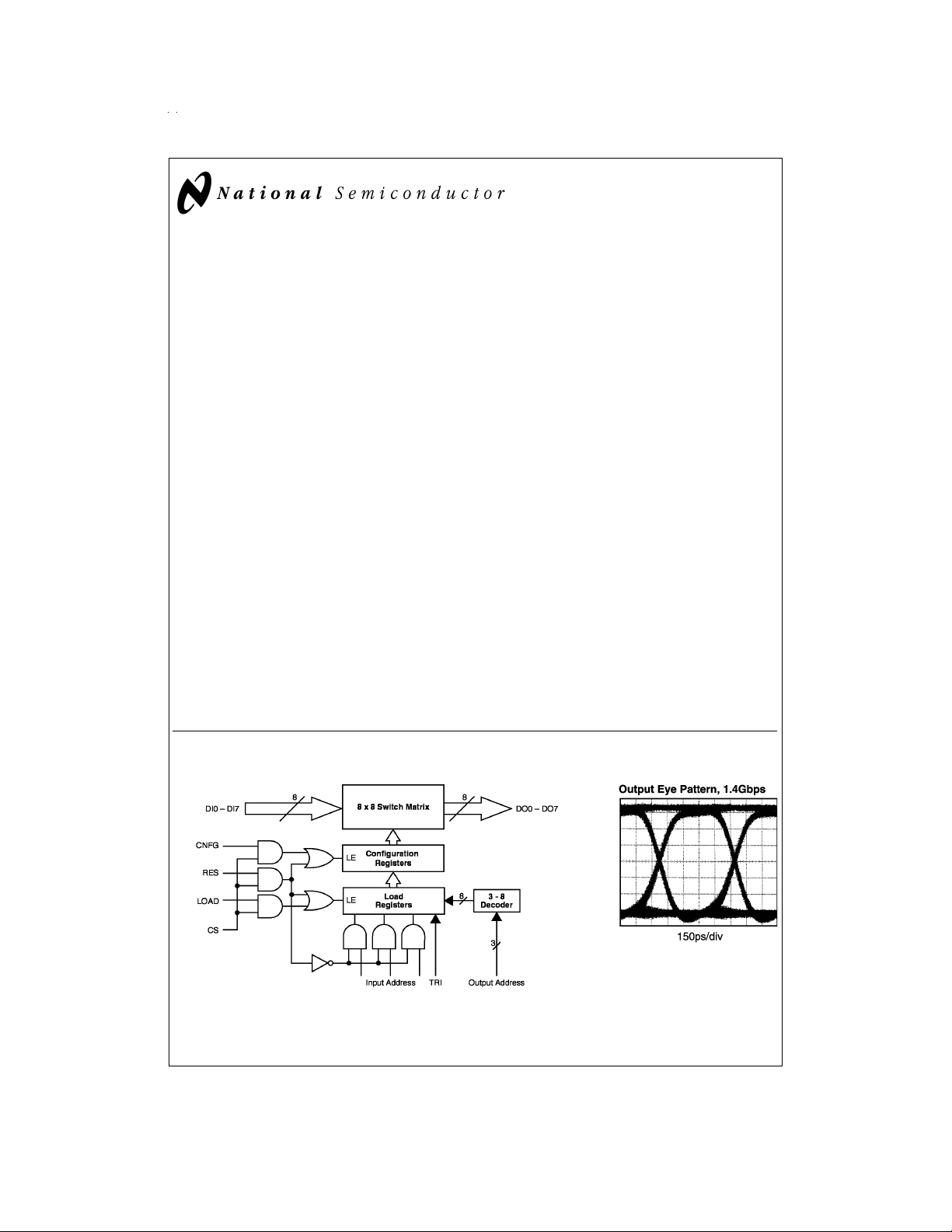
CLC018 Block Diagram
DS100088-1
DS100088-2
© 1998 National Semiconductor Corporation DS100088 www.national.com
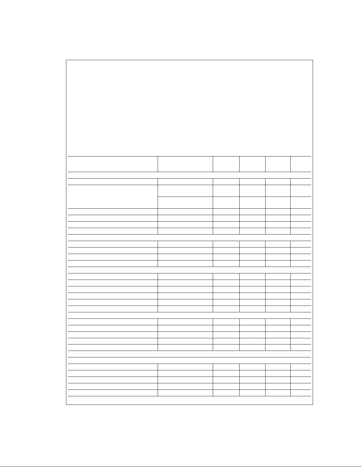
Absolute Maximum Ratings (Note 1)
If Military/Aerospace specified devices are required,
please contact the National Semiconductor Sales Office/
Distributors for availability and specifications.
Supply Voltage (V
Maximum VCC+6V
V
LL
Minimum VCC−0.5V
V
LL
CC–VEE)
Storage Temperature Range −65˚C to +150˚C
Lead Temp. (Soldering 4 sec.) +260˚C
ESD Rating TBD
Package Thermal Resistance
64-Pin PQFP 75˚C/W
θ
JA
−0.3V to +6.0V
θ
64-Pin PQFP 15˚C/W
JC
Reliability Information
Transistor Count 3000
MTTF (based on limited life test data) TBD
Recommended Operating
Conditions
Supply Voltage (VCC–VEE) 4.5V to 5.5V
Operating Temperature −40˚C to +85˚C
V
LL
VCCor VCC+5V
Electrical Characteristics
(VCC= 0V, VEE= −5V, VLL= 0V; unless otherwise specified) (Note 4).
Parameter Conditions
Typ
+25˚C
Min/Max
+25˚C
DYNAMIC PERFORMANCE
Max. Data Rate/Channel (NRZ) (Note 5) 1.4 Gbps
<
Channel Jitter Data Rate
(Note 6)
Data Rate<1.4 Gbps
(Note 6)
500 Mbps
50 ps
100 ps
Propagation Delay (input to output) 0.75 ns
Propagation Delay Match (Note 7)
±
200 ps
Output Rise/Fall Time (Note 8) 250 ps
Duty Cycle Distortion (Note 9) 10 ps
CONTROL TIMING: CONFIGURATION
OA Bus to LOAD
LOAD
to OA Bus Hold Time (T2)0ns
↓
IA Bus, TRI to LOAD
LOAD
to IA Bus, TRI Hold Time (T4)5ns
↓
Min Pulse Width: (T
Setup Time (T1)15ns
↑
Setup Time (T3)5ns
↓
)
5
LOAD 10 ns
CNFG 10 ns
LOAD
to CNFG↑Delay (T6)0ns
↑
CNFG
to Valid Delay (T7)20ns
↑
CNFG
to Output TRI-STATE Delay (T8)20ns
↑
CNFG
to Output Active Delay (T9)70ns
↑
CONTROL TIMING: RESET (Note 11)
TRI to RES
RES
Min Pulse Width: RES (T
RES
RES
Setup Time (T10)5ns
↑
to TRI Hold Time (T11)5ns
↓
)10ns
to TRI-STATE Mode Delay (T13)20ns
↑
to Broadcast Mode Delay (T14)70ns
↑
12
STATIC PERFORMANCE
Signal I/O:
Min Input Swing, Differential (Note 3) 150 200 200 mV
Input Voltage Range Lower Limit −2 V
Input Voltage Range Upper Limit 0.4 V
Input Bias Current (Notes 3, 12) 1.5 0.4/3.1 0.3/3.8 µA/output
Output Current (Note 3) 10.7 8.53/12.80 7.20/14.3 mA
Min/Max
−40˚C to
+85˚C
Units
PP
PP
PP
www.national.com 2
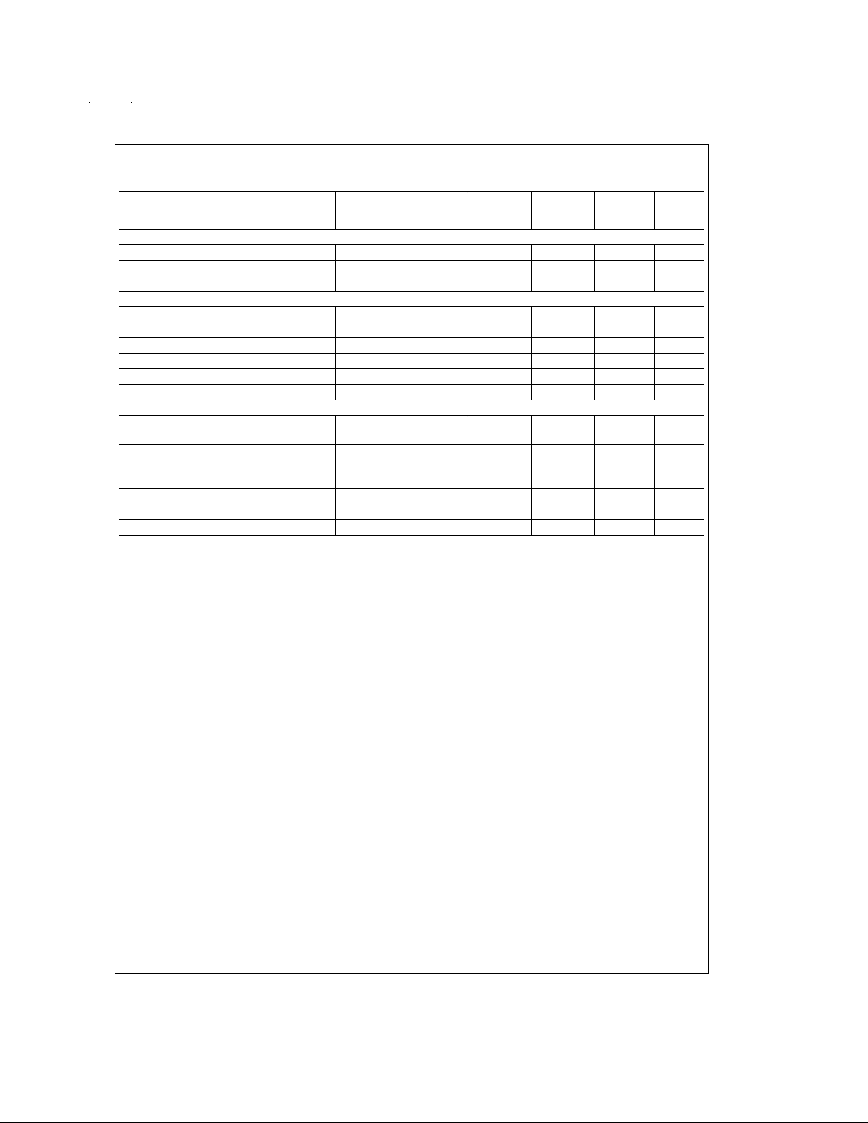
Electrical Characteristics (Continued)
(VCC= 0V, VEE= −5V, VLL= 0V; unless otherwise specified) (Note 4).
Parameter Conditions
Typ
+25˚C
Min/Max
+25˚C
Signal I/O:
Output Voltage Swing R
=75Ω 800 640/960 540/1060 mV
LOAD
Output Voltage Range Lower Limit −2.5 V
Output Voltage Range Upper Limit 0 V
Control Inputs:
Input Voltage - HIGH V
Input Voltage - LOW V
Input Voltage - HIGH V
Input Voltage - LOW V
IH min
IL max
IH min
IL max
Input Current - HIGH V
Input Current - LOW V
(Note 3) −1 −0.5 −0.5 V
(Note 3) −4 −4.5 −4.5 V
VLL= +5V (Note 3) 4 4.5 4.5 V
VLL= +5V (Note 3) 1 0.5 0.5 V
(Note 3) 1 0.2/2.0 0.1/2.5 µA
IH=VLL
−5V (Note 3) −100 −200/10 −250/15 µA
IL=VLL
MISCELLANEOUS PERFORMANCE
V
Supply Current All Outputs Active
CC
Supply Current All Outputs TRI-STATE
V
CC
Supply Current VLL= 0V (Note 3) 2.5 1.7/3.3 1.5/3.5 mA
V
LL
V
Supply Current VLL= +5V (Note 3) 7 mA
LL
(Notes 3, 13, 14)
(Note 3)
157 127/202 119/217 mA
7 3/11 2/12 mA
Input Capacitance 1.5 pF
Output Capacitance 2 pF
Note 1: “Absolute Maximum Ratings” are those values beyond which the safety of the device cannot be guaranteed. They are not meant to imply that the devices
should be operated at these limits. The table of “Electrical Characteristics” specifies conditions of device operation.
Note 2: Min/max ratings are based on product characterization and simulation. Individual parameters are tested as noted. Outgoing quality levels are determined
from tested parameters.
Note 3: J-level spec. is 100%tested at +25˚C.
Note 4: V
Note 5: Bit error rate less than 10
Note 6: Measured using a pseudo-random (2
Note 7: Spread in propagation delays for all input/output combinations.
Note 8: Measured between the 20%and 80%levels of the waveform.
Note 9: Difference in propagation delay for output low-to-high vs. output high-to-low transition.
Note 10: Refer to the
Note 11: Refer to the
Note 12: The bias current for high speed data input depends on the number of data outputs that are selecting that input.
Note 13: The V
Note 14: I
and all VEEsupply pins are bypassed with 0.01 µF ceramic capacitor.
LL
supply current is a function of the number of active data outputs. I
CC
VEE=IVCC+IVLL
−9
over 50%of the bit cell interval.
23
−1 pattern) binary sequence with all other channels active with an uncorrelated signal.
Configuration Timing Diagram
Reset Timing Diagram
.
.
.
18*N+7mAwhere N is an integer from 0 to 8.
VCC
Min/Max
−40˚C to
+85˚C
Units
www.national.com3
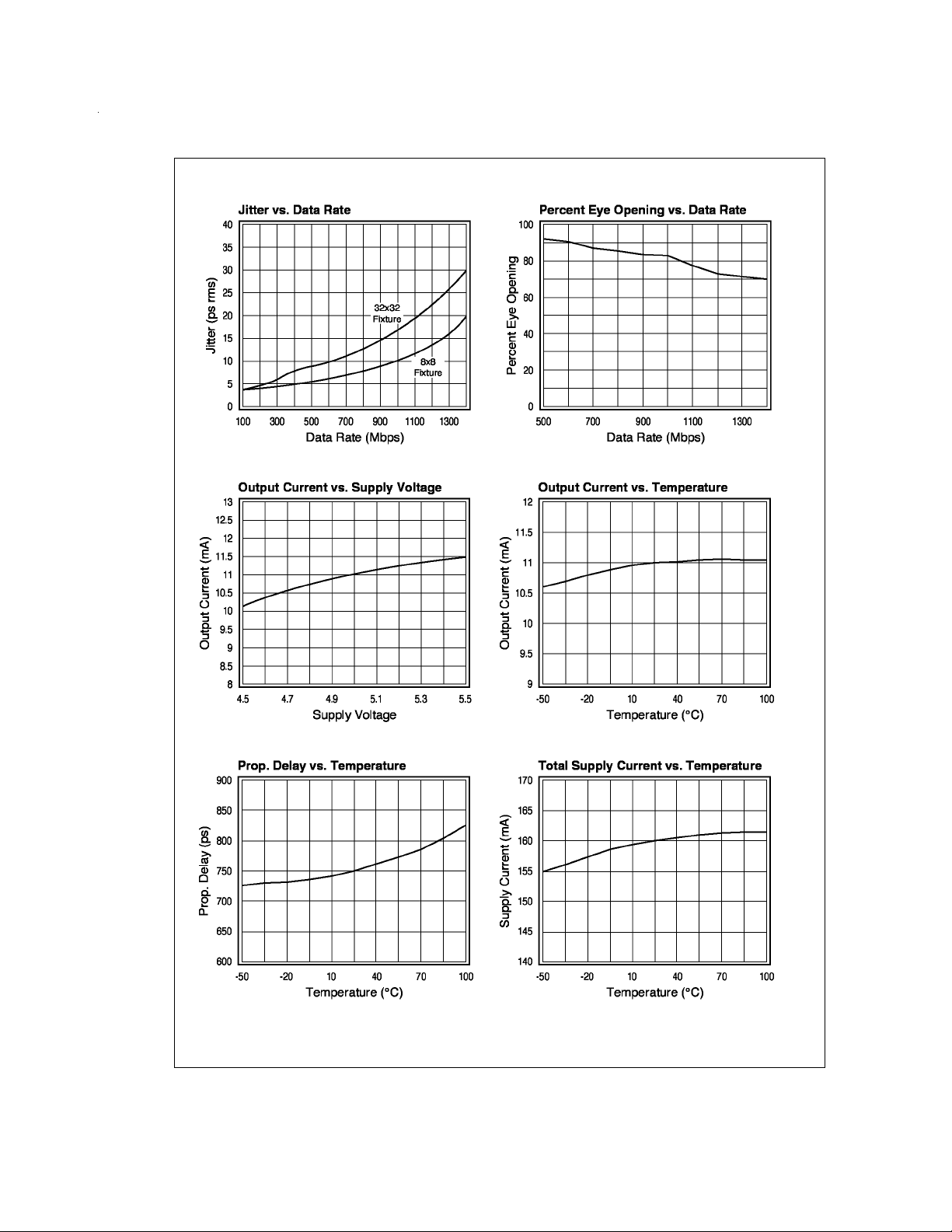
Typical Performance Characteristics
DS100088-3 DS100088-4
DS100088-5 DS100088-6
DS100088-7 DS100088-8
www.national.com 4
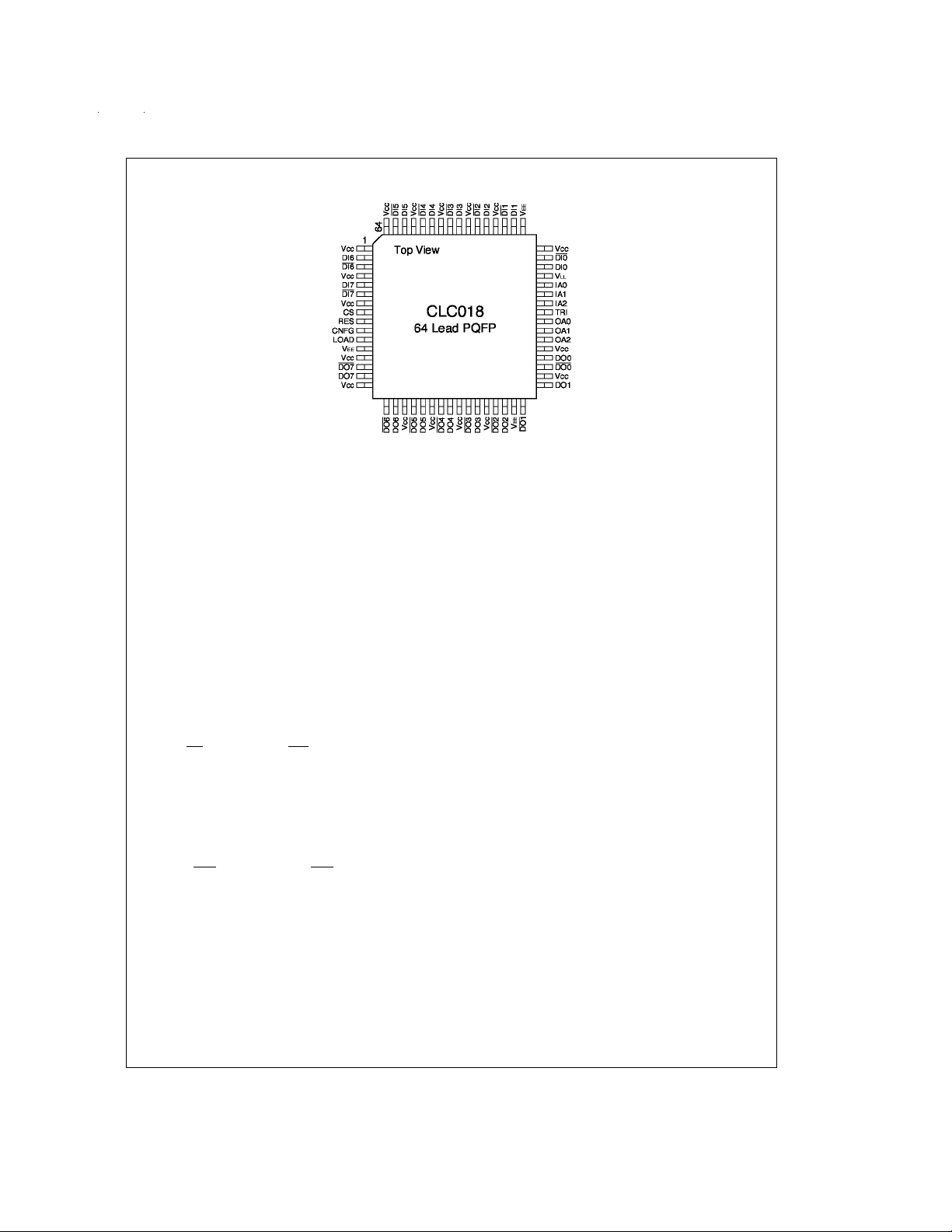
Connection Diagram
Order Number CLC018AJVJQ
See NS Package Number VJE64A
Pin Descriptions
POWER PINS
is the most positive rail for the data path. When the data
V
CC
levels are ECL compatible, then V
GND. For PECL data (+5V referenced ECL), V
nected to the +5V supply. Please refer to the device operation section in this datasheet for recommendations on the
bypassing and ground/power plane requirements of this device.
V
is the most negative rail for the data path. When the data
EE
levels are ECL compatible, then V
power supply. For PECL data (+5V referenced ECL), V
connected to GND.
V
is the logic-level power supply. If the control signals are
LL
referenced to +5V, V
trol signals are ECL compatible, V
is connected to a +5V supply. If con-
LL
DATA INPUT PINS
DI0 and DI0 through DI7 and D17 are the data input pins to
the CLC018. Depending upon how the Power pins are connected (please refer to the Power Pin section above) the
data may be either differential ECL, or differential PECL. To
drive the CLC018 inputs with a single-ended signal, please
refer to the section “Using Single-Ended Data” in the OPERATION section of this datasheet.
DATA OUTPUT PINS
DO0 and DO0 through DO7 and DO7 are the data output
pins of the CLC018. The CLC018 outputs are differential current outputs which can be converted to ECL or PECL compatible outputs through the use of load resistors. Please refer to the “Output Interfacing” paragraph in the OPERATION
section of this datasheet for more details.
should be connected to
CC
is connected to a −5.2V
EE
is connected to GND.
LL
CC
is con-
EE
DS100088-9
CONTROL PINS
IA2, IA1 and IA0 are the three bit input selection address
bus. The input port to be addressed is placed on this bus.
IA2 is the Most Significant Bit (MSB). If input port 6 is to be
addressed, IA2, IA1, IA0 should have 1, 1, 0 asserted on
them. The IA bus should be driven with CMOS levels, if V
is +5V. These levels are thus +5V referenced (standard
CMOS). If V
erenced to the −5V and GND supplies.
is connected to GND, the input levels are ref-
LL
OA2, OA1 and OA0 are the output selection address bus.
The output port selected by the OA bus is connected to the
input port selected on the IAbus when the data is loaded into
the configuration registers. OA2 is the MSB. If OA2, OA1,
is
OA0 are set to 0, 0, 1; then output port 1 will be selected.
CS is an active-high chip select input. When CS is high, the
RES, LOAD, and CNFG pins will be enabled.
LOAD is the latch control for the LOAD register. When LOAD
is high, the load register is transparent. Outputs follow the
state of the IA bus, and are presented to the inputs of the
Configuration register selected by the OA bus. When LOAD
is low, the outputs of the Load register are latched.
RES is the reset control of the configuration and load registers. A high-going pulse on the RES pin programs the switch
matrix to one of two possible states: with TRI low, all outputs
are connected to input #0; with TRI high, all outputs are put
in TRI-STATE condition.
TRI will program the selected output to be in a high impedance or TRI-STATE condition. To place an output in
TRI-STATE, assert a logic-high level on the TRI input when
the desired input and output addresses are asserted on the
respective address inputs and strobe the LOAD input as depicted in the ”Configuration Truth Table”. To enable an output, assert a logic-low level on the TRI input together with the
appropriate addresses and strobe the LOAD input as previously described.
CNFG is the configuration register latch control. When
CNFG is high the Configuration register is made transparent,
and the switch matrix is set to the state loaded into the Load
registers. When CNFG is low, the state of the switch matrix
is latched.
LL
www.national.com5
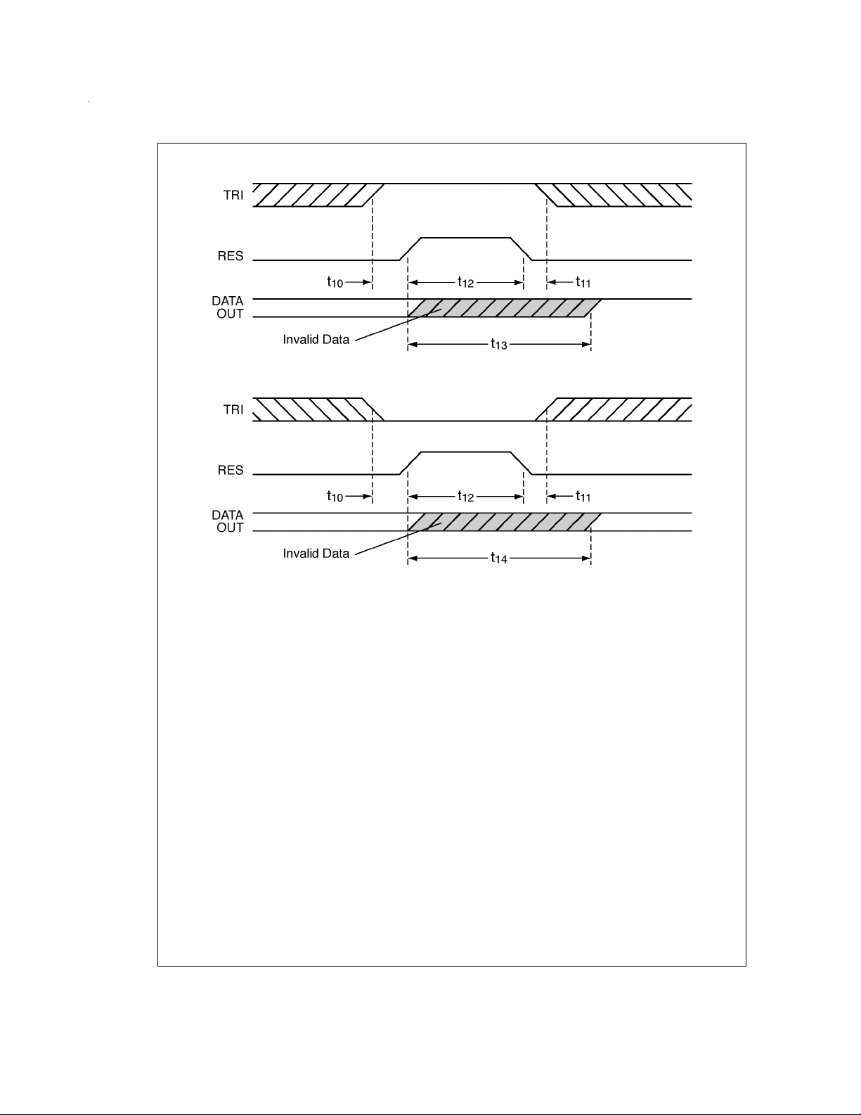
Timing Diagrams
DS100088-10
FIGURE 1. Timing Diagram —TRI-STATE Reset
DS100088-11
FIGURE 2. Timing Diagram —“Broadcast Reset”
www.national.com 6
 Loading...