NSC CLC012AJE-TR13, CLC012AJE Datasheet
CLC012
Adaptive Cable Equalizer for ITU-T G.703 Data Recovery
General Description
National’s CLC012 adaptive cable equalizer is a low-cost
monolithic solution for equalizing data transmitted over cable
(or any media with similar dispersive loss characteristics).
The CLC012 simplifies the task of high-speed data recovery
with a one-chip solution and a minimal number of external
components. The equalizer automatically adapts to equalize
any cable length from zero meters to lengths that attenuate
the signal by 40 dB at 200 MHz. This corresponds to 300
meters of Belden 8281 or 120 meters of Category 5 UTP
(unshielded twisted pair).
The CLC012 provides superior jitter performance: 180ps
pp
for 270 Mbps data that has passed through 200 meters of
Belden 8281 cable. This exceptional performance provides
wide error marginindigitaldatalinks.The equalizer operates
on a single supply with a power consumption of only 290
mW.The small 14-pin SOIC package allows for high-density
placement of components for multi-channel applications
such as routers.The equalizer operates over a wide range of
data rates from less than 50 Mbps to rates in excess of 650
Mbps.
The equalizer is flexible in allowing either single-ended or
differential input drive. Its high common mode rejection provides excellent immunity to interference from noise sources.
On-chip quantized feedback eliminates baseline wander.
Additional features include a Loss of Signal output and an
output mute pin which, when tied together, mute the output
when no signal is present. A buffered eye monitor output is
provided, for viewing the equalized signal prior to the com-
parator. Differential AEC pins allow the user to set the internal adaptive loop time constant with one external capacitor.
Features
n Automatic equalization of coaxial and twisted pair cables
n Loss of Signal detect and output mute
n Output eye monitor
n Single supply operation: +5V or −5.2V
n Single-ended or differential input
n Low cost
Applications
n ITU-T G.703 serial data recovery
n Serial digital data routing and distribution
n Serial digital data equalization and reception
n Data recovery equalization: ATM, CAD networks,
medical, set top terminals, industrial video networks
Key Specifications
n Low jitter: 180ps
pp
@
270 Mbps through 200 meters of
Belden 8281 coaxial cable
n High data rates:
<
50 Mbps to>650 Mbps
n Excellent input return loss: 19 dB
@
270 MHz
n Low supply current: 68 mA
n Equalizes up to 300+ meters of Belden 8281 or 120
meters of Cat 5 UTP cable
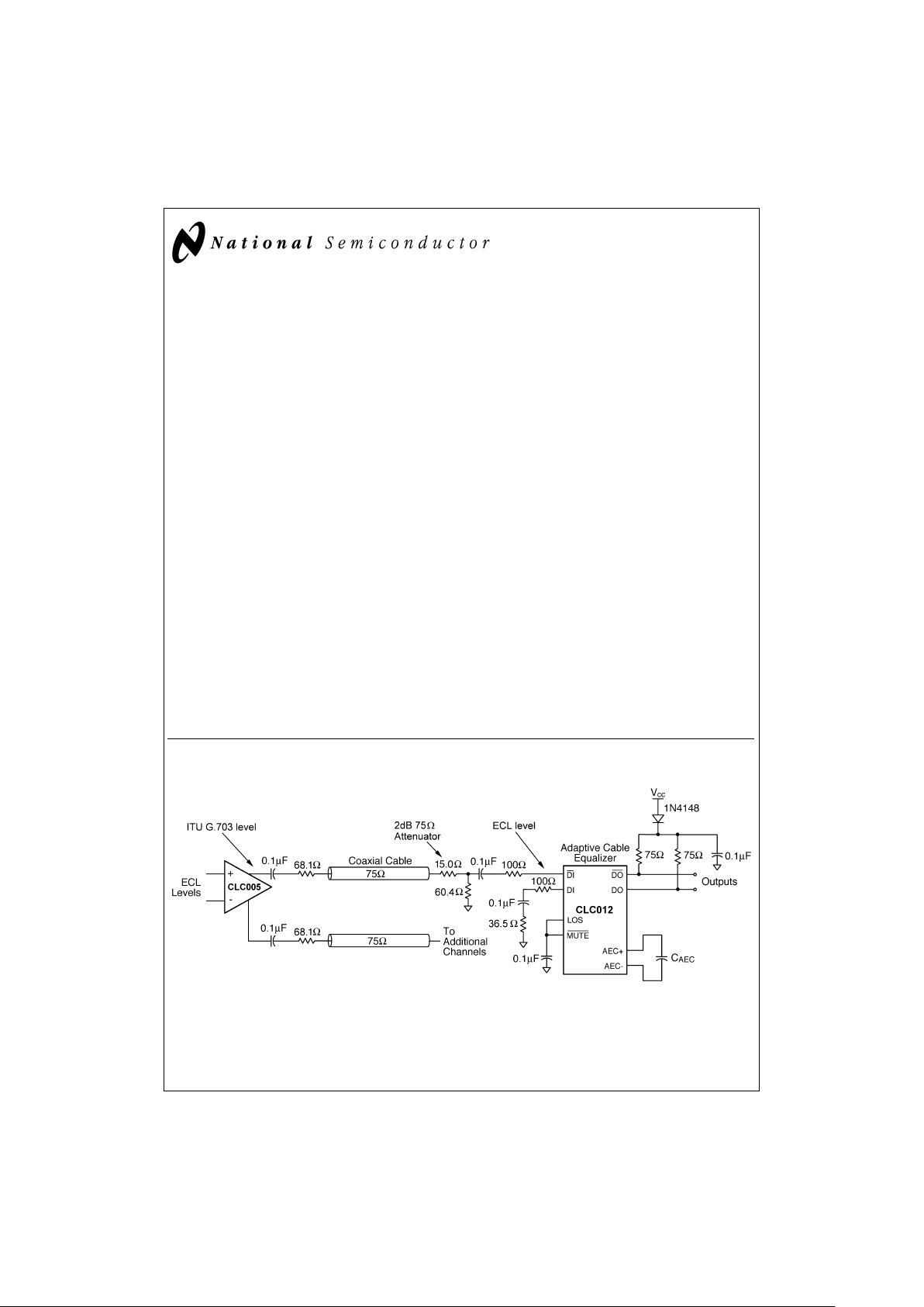
Typical Application
DS100145-4
August 1998
CLC012 Adaptive Cable Equalizer for ITU-T G.703 Data Recovery
© 1998 National Semiconductor Corporation DS100145 www.national.com
Typical Application (Continued)
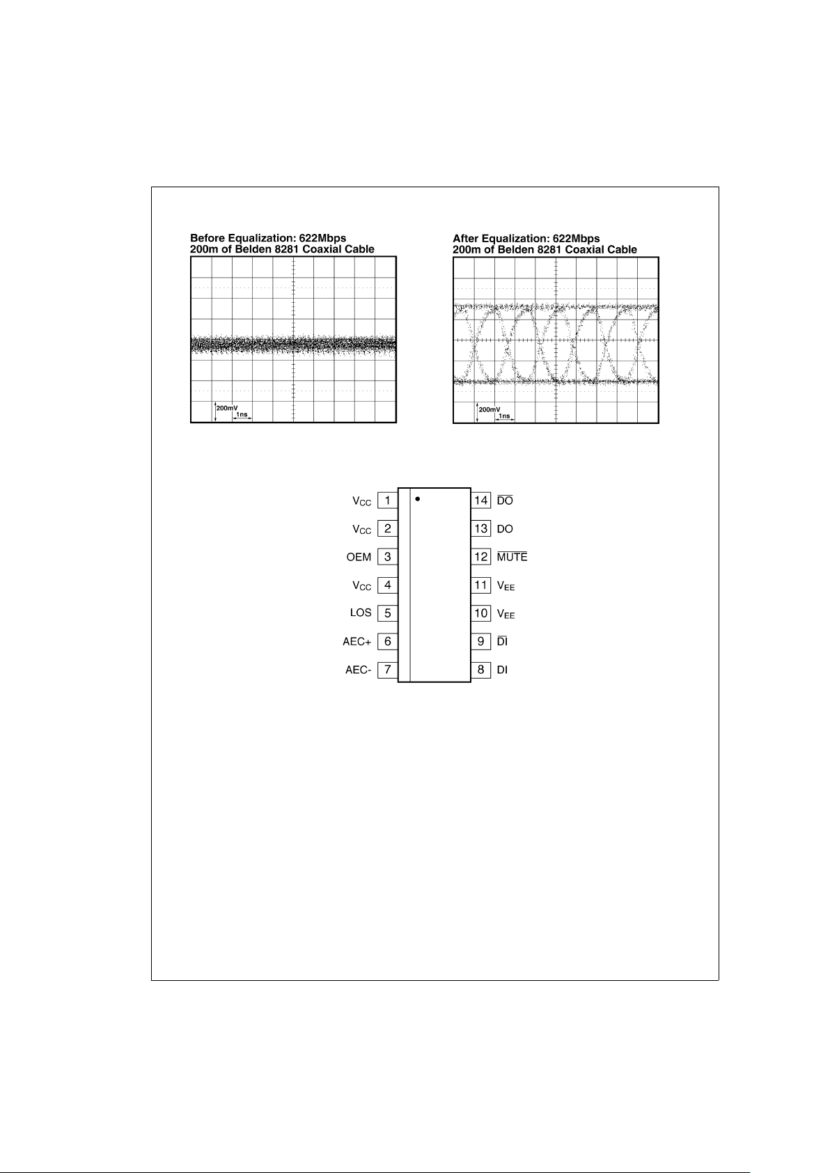
Connection Diagram
DS100145-2
DS100145-3
Pinout SOIC
DS100145-1
14-Pin SOIC
Order Number CLC012AJE
See NS Package Number M14A
www.national.com 2
Absolute Maximum Ratings (Note 1)
If Military/Aerospace specified devices are required,
please contact the National Semiconductor Sales Office/
Distributors for availability and specifications.
Supply Voltage (V
CC–VEE
) −0.3V, +6.5V
Maximum Junction Temperature +150˚C
Storage Temperature Range −65˚C to +150˚C
Lead Temperature
(Soldering 4 sec.) +260˚C
ESD Rating (Note 14) ≥500V
θ
JA
14-Pin SOIC (AJE) 95˚C/W
MTTF (based on limited life test
data)
4.8x10
7
hours
Recommended Operating
Conditions
Supply Voltage (VCC–VEE) 4.5V to 5.5V
Operating Temperature Range −40˚C to +85˚C
Series Input Resistance
(In Series w/DI & DI)
100Ω
Input Coupling Capacitance 0.1 µF
AEC Capacitor (Connected
between AEC+ & AEC−) 50 pF to 1 µF
Cable Input Voltage Swing
(Note 4) 720 to 880 mV
pp
DO/DO Minimum Voltage
(Note 15) VCC–1.6V
Electrical Characteristics
(VCC= +5V, VEE= 0V, signal source swing = 0.8 Vpp(Note 4), C
AEC
= 100 pF)
Parameter Conditions
Typ
+25˚C
Min/Max
+25˚C
Min/Max
−40˚C to
+85˚C
Units
DYNAMIC PERFORMANCE
Residual Jitter
10 meters Belden 8281 311 Mbps PRN (Note 5) 150 250 400 ps
pp
300 meters Belden 8281 311 Mbps PRN (Notes 3, 5) 350 500 750 ps
pp
Equalization Time Constant
100 meters Belden 8281 C
AEC
= 100 pF (Note 6) 1.5 _ _ µs
200 meters Belden 8281 C
AEC
= 100 pF (Note 6) 2.0 _ _ µs
300 meters Belden 8281 C
AEC
= 100 pF (Note 6) 3.2 _ _ µs
output rise and fall time (20%–80%)R
collector
=75Ω 750 _ _ ps
output duty cycle distortion 30 _ _ ps
minimum average transition density 1/50 _ _ trans/ns
maximum average data rate 150m Belden 8281 (Note 7) 650 _ _ Mbps
V
CC
Jitter Sensitivity
27 MHz 0.85 _ _ ns/V
270 MHz 1.90 _ _ ns/V
V
EE
Jitter Sensitivity
27 MHz 0.55 _ _ ns/V
270 MHz 1.45 _ _ ns/V
STATIC PERFORMANCE
Supply Current (Includes Output Current)
V
AEC
= 0V (Note 3) 68 48/75 40/80 mA
V
AEC
= 0.4V (Note 3) 53 43/64 37/70 mA
Input and Output Parameters
DO/DO output current
10 8.7/11.3 8.0/12 mA
DO/DO output voltage swing
R
collector
=75Ω(Note 3) 750 650/850 600/900 mV
DI/DI common mode voltage
3.4 _ _ V
AEC differential voltage Belden 8281 1.5 _ _ mV/meter
AEC+/AEC− common mode 3.6 _ _ V
output eye monitor (OEM) bias potential 3.2 _ _ V
Loss of Signal (LOS) current output-HIGH LOS V
OH
= 4.5V −400 _ _ µA
Loss of Signal (LOS) current output-LOW LOS V
OL
= 0.5V 600 _ _ µA
MUTE voltage input-HIGH
(Note 3) 1.8 2.0 2.0 V
MUTE voltage input-LOW
(Note 3) 1.2 0.8 0.8 V
3 www.national.com

Electrical Characteristics (Continued)
(VCC= +5V, VEE= 0V, signal source swing = 0.8 Vpp(Note 4), C
AEC
= 100 pF)
Parameter Conditions
Typ
+25˚C
Min/Max
+25˚C
Min/Max
−40˚C to
+85˚C
Units
Input and Output Parameters
MUTE current input-HIGH
VIH= 5V (Note 3) 5.0
±
100
±
500 nA
MUTE current input-LOW
VIL= 0V (Note 3) 0.2
±
100
±
500 nA
TIMING PERFORMANCE
LOS Response Time
carrier applied (Note 8) 150 1000 1000 ns
carrier removed (Note 9) 150 1000 1000 ns
MUTE response time
(Note 10) 2.0 _ _ ns
MISCELLANEOUS PERFORMANCE
input resistance single-ended 7.3 _ _ kΩ
input capacitance single-ended (Note 11) 1.0 _ _ pF
input return loss
@
270 MHz Zo=75Ω(Note 12) 19 _ _ dB
maximum cable attenuation 200 MHz (Note 13) 40 _ _ dB
Note 1: “Absolute Maximum Ratings” are those values beyond which the safety of the device cannot be guaranteed. They are not meant to imply that the devices
should be operated at these limits. The table of “Electrical Characteristics” specifies conditions of device operation.
Note 2: Min/max ratings are based on product characterization and simulation. Individual parameters are tested as noted. Outgoing quality levels are determined
from tested parameters.
Note 3: J-level: spec. is 100%tested at +25˚C.
Note 4: These specifications assume an 800 mV
pp
signal at the cable input. Levels above and below 800 mV are allowable, but performance may vary. The cable
will attenuate the signal prior to entering the equalizer.
Note 5: Peak-to-peak jitter is defined as 6 times the rms jitter.
Note 6: For more information, see “CLC012 Operation” and “Design Guidelines”.
Note 7: 50%eye opening.
Note 8: Time from application of a valid signal to when the LOS output asserts high.
Note 9: Time from the removal of a valid signal to when the LOS output asserts low.
Note 10: Time from assertion of MUTE to when the output responds.
Note 11: Device only. Does not include typical pc board parasitics.
Note 12: Includes typical pc board parasitics.
Note 13: This sets the maximum cable length for the equalizer.
Note 14: Human body model, 1.5 kΩ in series with 100 pF; based on limited test data.
Note 15: To maintain specified performance, do not reduce DO/DO below this level.
www.national.com 4
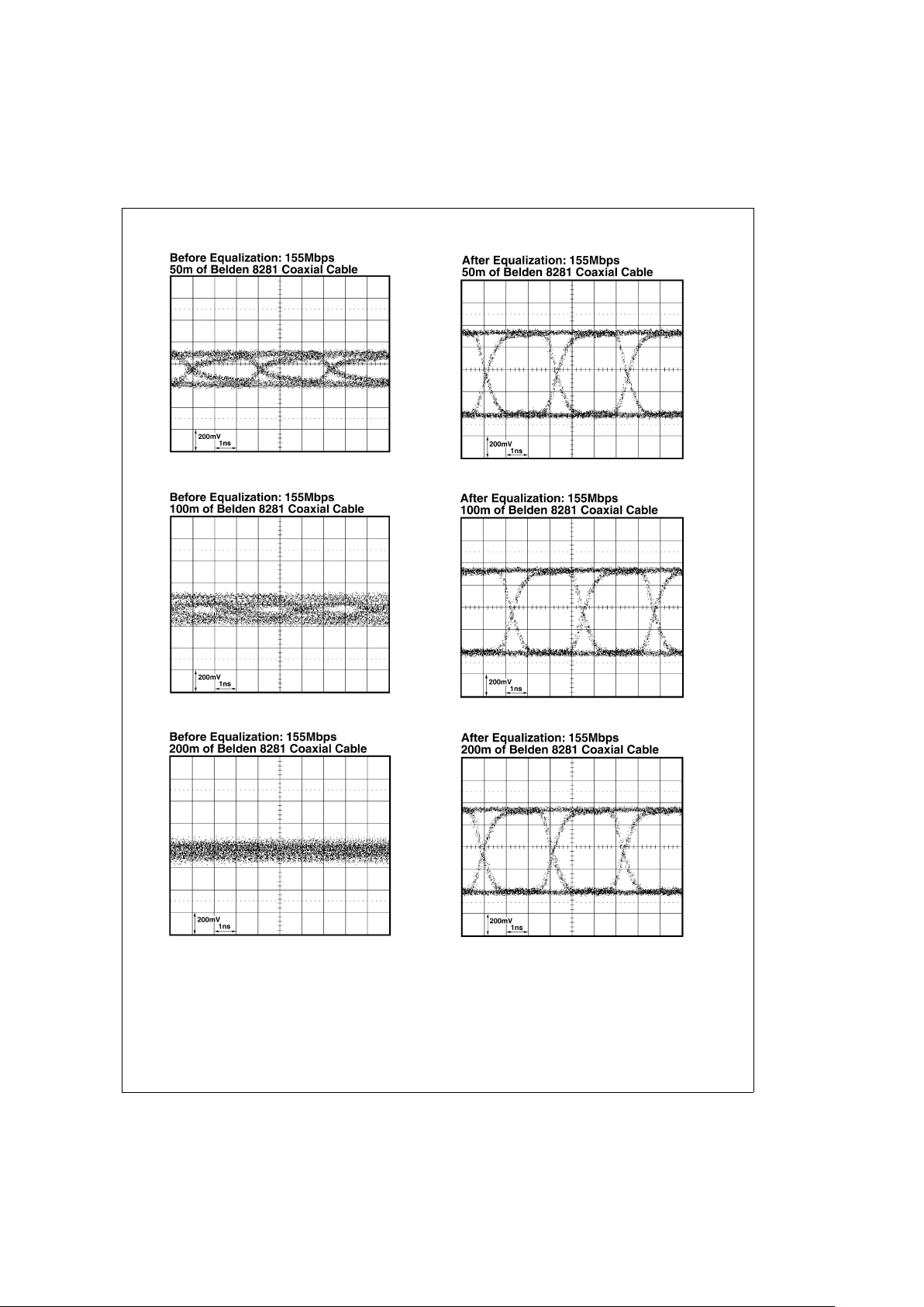
Typical Performance Characteristics
DS100145-5
DS100145-9
DS100145-6
DS100145-10
DS100145-7
DS100145-11
5 www.national.com
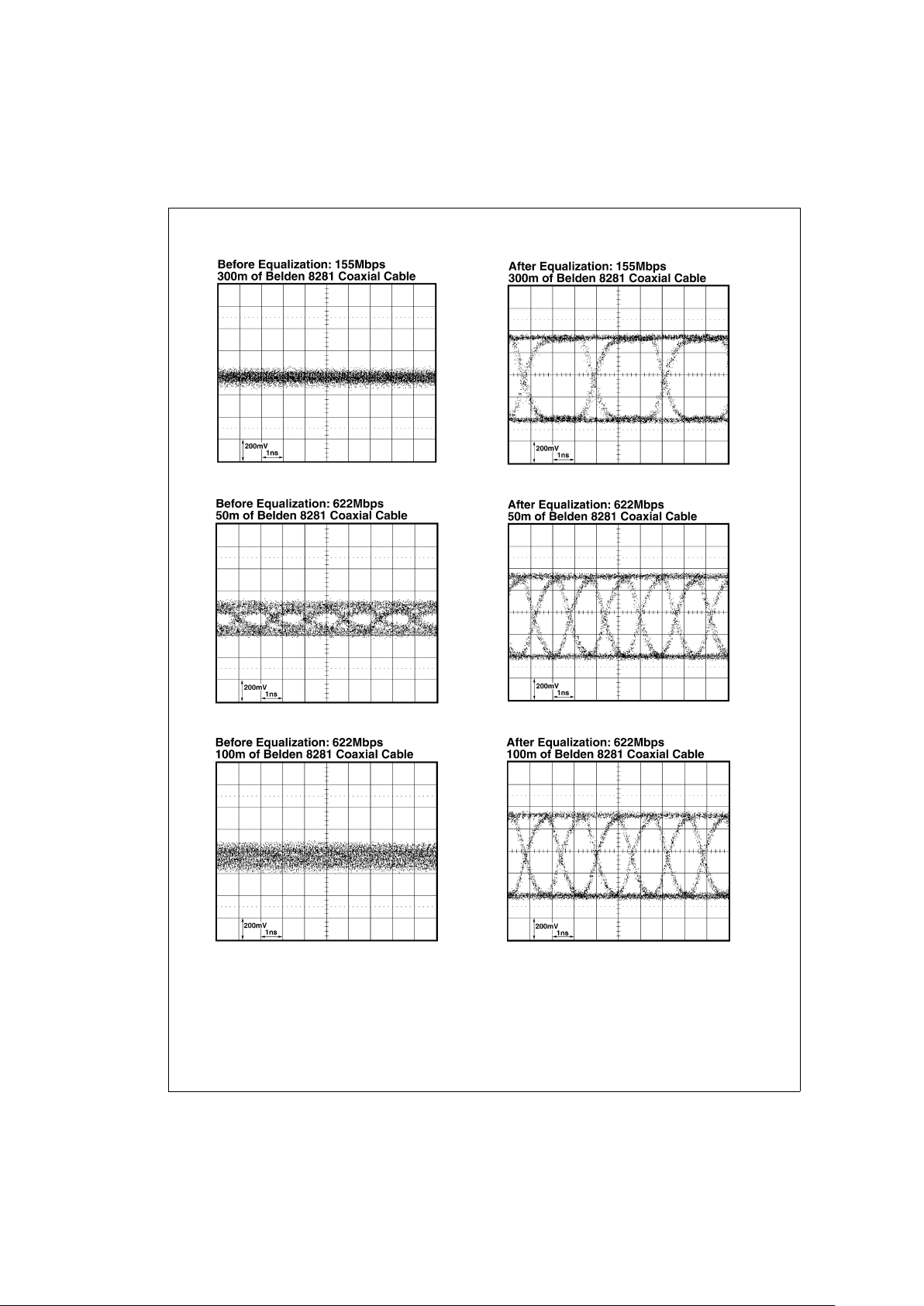
Typical Performance Characteristics (Continued)
DS100145-8
DS100145-12
DS100145-13
DS100145-16
DS100145-14
DS100145-39
www.national.com 6
 Loading...