NSC ADCV0831M6X, ADCV0831M6 Datasheet

ADCV0831
8 Bit Serial I/O Low Voltage Low Power ADC with
Auto Shutdown in a SOT Package
ADCV0831 8 Bit Serial I/O Low Voltage Low Power ADC with Auto Shutdown in a SOT Package
February 2000
General Description
TheADCV0831 is a low voltage 8-bit successive approximationA/D converter with serial I/O. The I/O is a 3-wire serial interface compatible with NSC’s MICROWIRE
SPI standards. It easily interfaces with standard shift registers or microprocessors.
Low voltage and auto shutdown features make the
ADCV0831 ideal for portable battery operated electronic devices. The main benefits are most apparent in small portable
electronic devices. The tiny A/D converter can be placed
anywhere on the board.
™
& Motorola’s
Applications
n Digitizing automotive sensors
n Process control monitoring
n Remote sensing in noisy environments
n Instrumentation
n Test systems
n Embedded diagnostics
Ordering Information
Temperature Range
(0˚C ≤ T
ADCV0831M6 MA06A 1k Units Tape and Reel
ADCV0831M6X MA06A 3k Units Tape and Reel
≤ +70˚C)
j
Features
n Tiny 6-pin SOT 23 package
n Serial digital data link requires few I/O pins
n Auto Shutdown
n 0V to 3V analog input range with single 3V power
supply
n TTL/CMOS input/output compatible
Key Specifications
(For 3V supply, typical, unless otherwise noted.)
n Resolution: 8 bits
n Conversion time (f
n Low power dissipation: 720µW
n Single supply: 2.7V to 5V
n Linearity error:±1.5LSB over temperature
n No missing codes over temperature
n Shutdown supply current 10nA
Package Supplied As
= 700 kHz): 16µs
C
DC
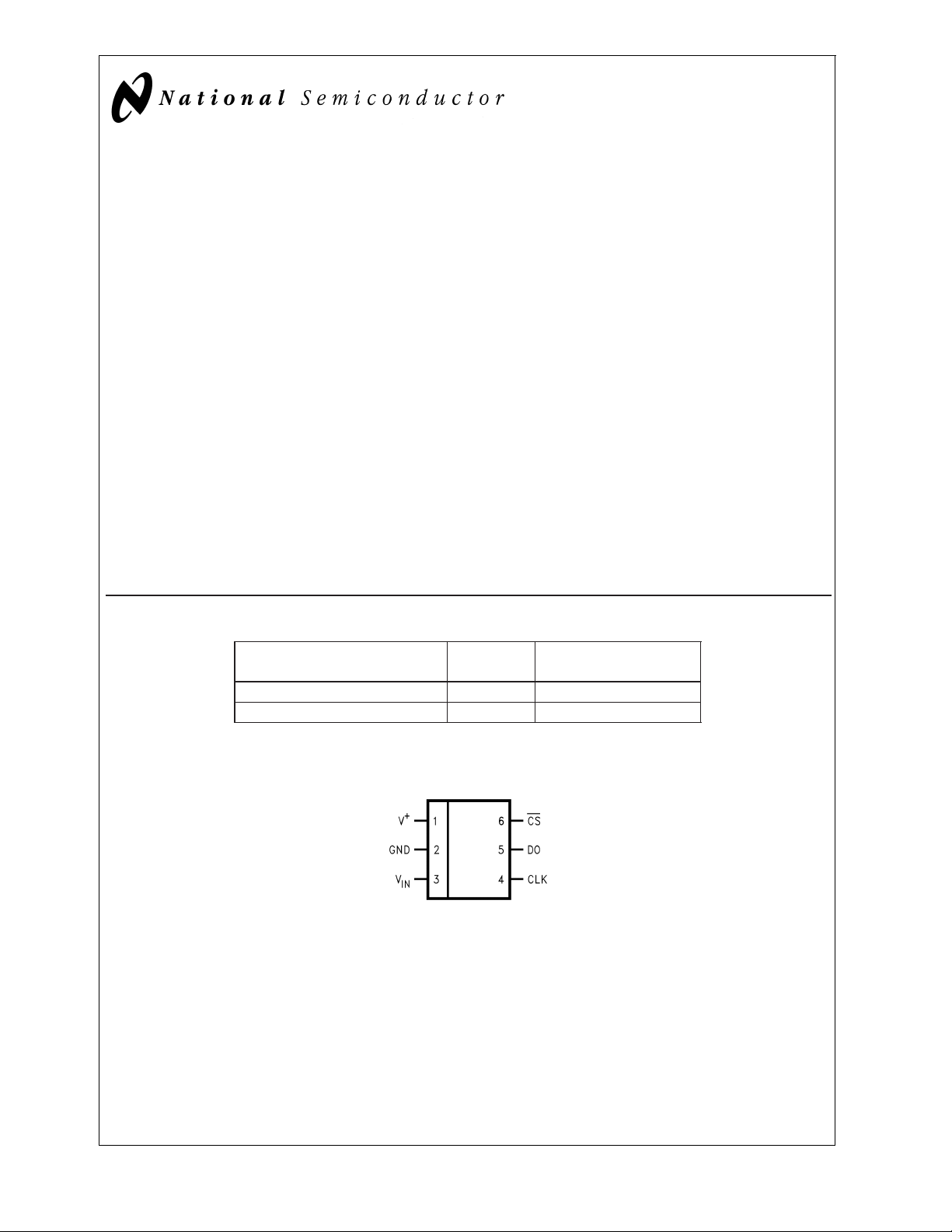
Connection Diagram
ADCV0831
DS100104-1
TRI-STATE®is a registered trademark of National Semiconductor Corporation.
™
COPS
microcontrollers and MICROWIRE™are trademarks of National Semiconductor Corporation.
© 2000 National Semiconductor Corporation DS100104 www.national.com

Absolute Maximum Ratings (Notes 1, 3)
If Military/Aerospace specified devices are required,
please contact the National Semiconductor Sales Office/
ADCV0831
Distributors for availability and specifications.
Supply Voltage (V
Voltage at Inputs and Outputs −0.3V to V
Input Current at Any Pin (Note 4)
Package Input Current (Note 4)
Power Dissipation at T
) 5.5V
CC
CC
±
= 25˚C
A
+ 0.3V
±
(Note 5) 470 mW
ESD Susceptibility (Note 6) 2000V
Electrical Characteristics
The following specifications apply for VCC=3VDC, and f
TA=TJ=T
Symbol Parameter Conditions
V
IN
V
IN(1)
V
IN(0)
I
IN(1)
I
IN(0)
V
OUT(1)
V
OUT(0)
I
OUT
I
SOURCE
I
SINK
I
CC
MIN
to T
; all other limits TA=TJ= 25˚C.
MAX
Integral Linearity Error
Offset Error
Full Scale Error
Resolution 8 Bits (min)
Analog Input Voltage (VCC+ 0.05) V (max)
Logical “1” Input Voltage VCC=3V 2.0 V (min)
Logical “0” Input Voltage VCC=3V 0.8 V (max)
Logical “1” Input Current VIN= 3V 0.01 1 µA (max)
Logical “0” Input Current VIN= 0V 0.01 −1 µA (max)
Logical “1” Output Voltage I
Logical “0” Output Voltage I
TRI-STATE®Output Current V
Output Source Current V
Output Sink Current V
out
out
OUT
OUT
OUT
Supply Current CS = HIGH 0.01 30 µA (max)
CS = LOW
Soldering Temperature (Note 7)
Convection Infrared (15 sec.) 215˚C
Wave Soldering (4 sec.) (Note 7) 260˚C
Storage Temperature −65˚C to +150˚C
Thermal Resistance (θ
5mA
20 mA
Operating Ratings (Notes 2, 3)
Temperature Range 0˚C≤ T
Supply Voltage (V
= 500 kHz unless otherwise specified. Boldface limits apply for
CLK
Typical
(Note 8)
±
0.6
±
0.1
±
0.3
) 265˚C/W
JA
) 2.7VDCto 5V
CC
Limits
(Note 9)
±
1.5 LSB (max)
±
1.5 LSB (max)
±
1.5 LSB (max)
≤70˚C
j
Units
(GND − 0.05) V (min)
=-360µA 2.8 2.4 V (min)
=1.6 mA 0.24 0.4 V (max)
= 0V 0.01 3.0 µA (max)
= 0V 2.6 1.0 mA (min)
= 3V 7.4 3.0 mA (min)
200 400 µA (max)
AC Electrical Characteristics
The following specifications apply for VCC=+3VDC, and tr=tf= 20 ns unless otherwise specified. Boldface limits apply for
TA=TJ=T
Symbol Parameter Conditions Typical Limits Units
f
CLK
t
SET-UP
T
C
t
pd
t
1H,t0H
www.national.com 2
MIN
to T
; all other limits TA=TJ= 25˚C.
MAX
(Note 8) (Note 9)
Clock Frequency 700 kHz (max)
10 kHz (min)
CS failing edge to CLK rising edge 25 ns
Clock Duty Cycle 40 % (min)
60 % (max)
Conversion Time 11 Clock
CLK Falling Edge to Data Valid Low to High CL= 100 pF 142 250 ns (max)
High to Low 70 200
CS Rising Edge to Data Output TRI-STATE CL= 100 pF, RL=2
75 250 ns (max)
kΩ
(see TRI-STATE Test Circuits) C
= 100 pF, RL=10
L
50
kΩ
Periods

AC Electrical Characteristics (Continued)
The following specifications apply for VCC=+3VDC, and tr=tf= 20 ns unless otherwise specified. Boldface limits apply for
TA=TJ=T
MIN
to T
; all other limits TA=TJ= 25˚C.
MAX
Symbol Parameter Conditions Typical Limits Units
(Note 8) (Note 9)
C
IN
C
OUT
Note 1: Absolute Maximum Ratings indicate limits beyond which damage to the device may occur.
Note 2: Operating Ratings indicate conditions for which the device is functional. These ratings do not guarantee specific performance limits. For guaranteed speci-
fications and test conditions, see the Electrical Characteristics. The guaranteed specifications apply only for the test conditions listed. Some performance characteristics may degrade when the device is not operated under the listed test conditions.
Note 3: All voltages are measured with respect to GND = 0 V
Note 4: When the input voltage V
maximum package input current rating limits the number of pins that can safely exceed the power supplies with an input current of 5 mA to four pins.
Note 5: The maximum power dissipation must be derated at elevated temperatures and is dictated by T
allowable power dissipation at any temperature is P
Note 6: Human body model, 100 pF capacitor discharged through a 1.5 kΩ resistor.
Note 7: SeeAN450“SurfaceMountingMethodsandTheirEffectonProductReliability”orLinearDataBooksection“SurfaceMount”forothermethodsofsoldering
surface mount devices.
Note 8: Typicals are at T
Note 9: Guaranteed to National’s AOQL (Average Outgoing Quality Level).
Capacitance of Logic Inputs 5 pF
Capacitance of Logic Outputs 5 pF
, unless otherwise specified.
D
=(T
DC
JMAX−TA
)/θJAor the number given in the Absolute Maximum Ratings, whichever is lower.
at any pin exceeds the power supplies (V
IN
= 25˚C and represent the most likely parametric norm.
J
<
IN
GND or V
>
VCC) the current at that pin should be limited to 5 mA. The 20 mA
IN
, θJAand the ambient temperature, TA. The maximum
JMAX
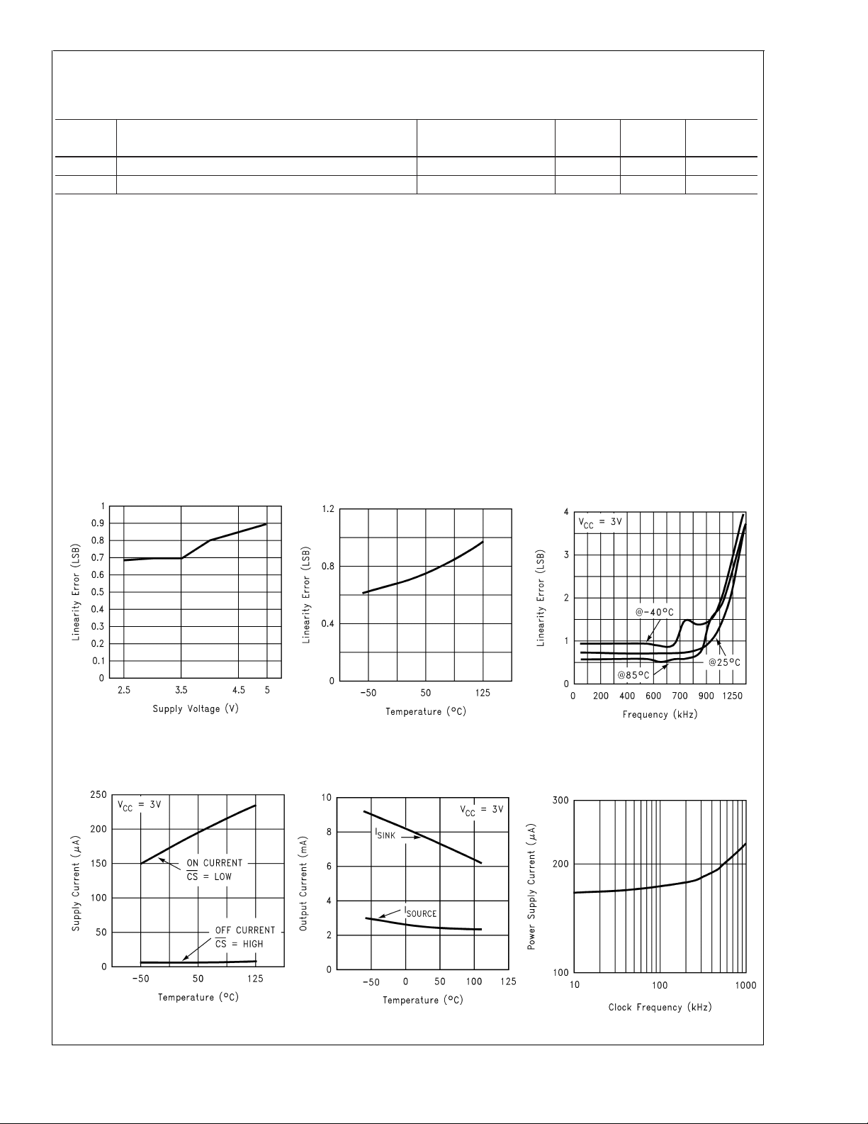
Typical Performance Characteristics
The following specifications apply for VCC= 3V, unless otherwise specified
ADCV0831
Integral Linearity Error vs
Supply Voltage
Power Supply Current
vs Temperature
DS100104-62
Linearity Error vs
Temperature
Output Current vs
Temperature
DS100104-56
Linearity Error vs
Clock Frequency
DS100104-55
Power Supply Current
vs Clock Frequency
DS100104-57
DS100104-58
DS100104-61
www.national.com3
 Loading...