NSC ADC16071CIWMX, ADC16071CIWM, ADC16071CIN Datasheet
TL/H/11454
ADC16071/ADC16471 16-Bit Delta-Sigma 192 ks/s Analog-to-Digital Converters
February 1995
ADC16071/ADC16471
16-Bit Delta-Sigma 192 ks/s Analog-to-Digital Converters
General Description
The ADC16071/ADC16471 are 16-bit delta-sigma analogto-digital converters using 64
c
oversampling at
12.288 MHz. A 5th-order comb filter and a 246 tap FIR decimation filter are used to achieve an output data rate of up to
192 kHz. The combination of oversampling and internal digital filtering greatly reduces the external anti-alias filter requirements to a simple RC low pass filter. The FIR filters
offer linear phase response, 0.005 dB passband ripple, and
t
90 dB stopband rejection. The ADC16071/ADC16471’s
analog fourth-order modulator uses switched capacitor
technology. A built-in fully-differential bandgap voltage reference is also included in the ADC16471. The ADC16071
has no internal reference and requires externally applied
reference voltages.
The ADC16071/ADC16471 use an advanced BiCMOS process for a low power consumption of 500 mW (max) while
operating from a single 5V supply. A power-down mode reduces the power supply current from 100 mA (max) in the
active mode to 1.3 mA (max).
The ADC16071/ADC16471 are ideal analog-to-digital front
ends for signal processing applications. They provide a
complete high resolution signal acquisition system that requires a minimal external anti-aliasing filter, reference, or
interface logic.
The ADC16071/ADC16471’s serial interface is compatible
with the DSP56001, TMS320, and ADSP2100 digital signal
processors.
Key Specifications
Y
Resolution 16 bits
Y
Total harmonic distortion
48 kHz output data rate
b
94 dB (typ)
192 kHz output data rate
b
80 dB (typ)
Y
Maximum output data rate 192 kHz (min)
Y
Power dissipation
Ð Active
192 kHz output data rate 500 mW (max)
48 kHz output data rate 275 mW (max)
Ð Power-down 6.5 mW (max)
Key Features
Y
Voltage reference (ADC16471 only)
Y
Fourth-order modulator
Y
64coversampling with a 12.288 MHz sample rate
Y
Adjustable output data rate from 7 kHz to 192 kHz
Y
Linear-phase digital anti-aliasing filter:
Ð 0.005 dB passband ripple
Ð 90 dB stopband rejection
Y
Singlea5V supply
Y
Power-down mode
Y
Serial data interface compatible with popular
DSP devices
Applications
Y
Medical instrumentation
Y
Process control systems
Y
Test equipment
Y
High sample-rate audio
Y
Digital Signal Processing (DSP) analog front-end
Y
Vibration and noise analysis
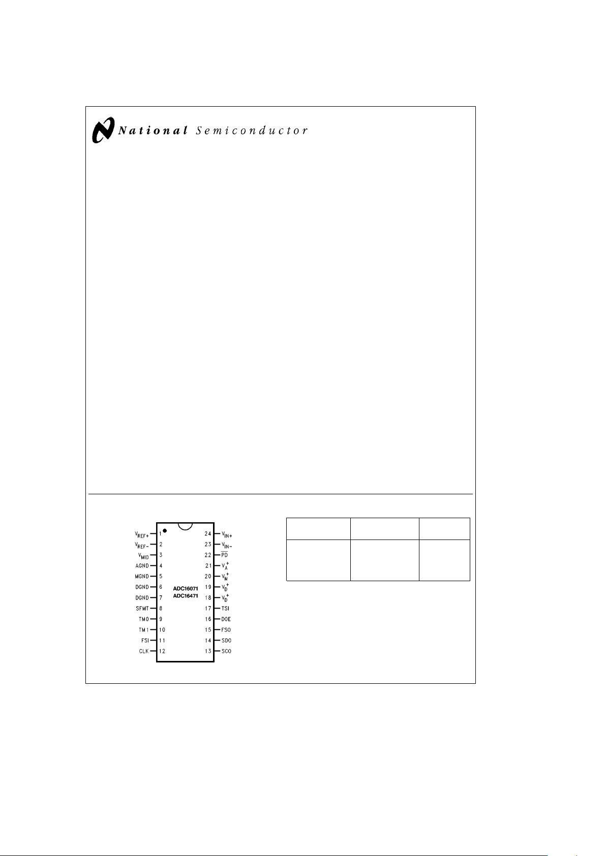
Connection Diagram
TL/H/11454– 2
Ordering Information
Part No. Package
NS Package
No.
ADC16471CIN 24-Pin Molded DIP N24C
ADC16471CIWM 24-Pin SOIC M24B
ADC16071CIN 24-Pin Molded DIP N24C
ADC16071CIWM 24-Pin SOIC M24B
TRI-STATEÉis a registered trademark of National Semiconductor Corporation.
C
1995 National Semiconductor Corporation RRD-B30M75/Printed in U. S. A.
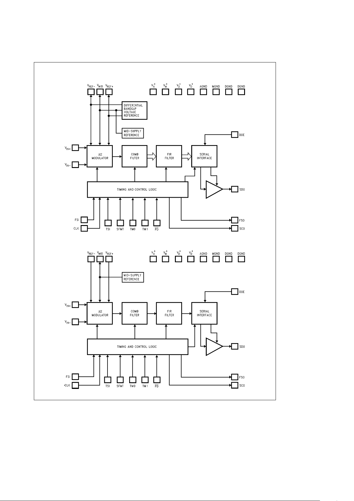
Block Diagram
ADC16471
TL/H/11454– 1
ADC16071
TL/H/11454– 22
2
Absolute Maximum Ratings (Notes 1 and 2)
If Military/Aerospace specified devices are required,
please contact the National Semiconductor Sales
Office/Distributors for availability and specifications.
Supply Voltage (V
A
a
,V
D
a
, and V
M
a
)
a
6.5V
Logic Control Inputs
b
0.3V to V
D
a
a
0.3V
Voltage at Other
Inputs and Outputs
b
0.3V to V
A
a
e
V
M
a
a
0.3V
Input Current at Any Pin (Note 3)
g
25 mA
Package Input Current (Note 3)
g
100 mA
Maximum Junction Temperature (Note 4) 150§C
Storage Temperature
b
65§Ctoa150§C
Lead Temperature
N Package (Soldering, 10 sec.) 300
§
C
WM Package (Infrared, 15 sec.) 220
§
C
WM Package (Vapor Phase, 60 sec.) 215
§
C
ESD Susceptibility (Note 5)
Human Body Model 4000V
Machine Model 250V
See AN-450 ‘‘Surface Mounting Methods and Their Effect
on Product Reliability’’ for other methods of soldering surface mount devices.
Operating Ratings (Notes 1 and 2)
Temperature Range
(T
min
s
T
A
s
T
max
)
ADC16471CIN, ADC16071CIN,
b
40§CsT
A
s
a
85§C
ADC16471CIWM, ADC16071CIWM
Supply Voltage
V
A
a
,V
D
a
,V
M
a
4.75V to 5.25V
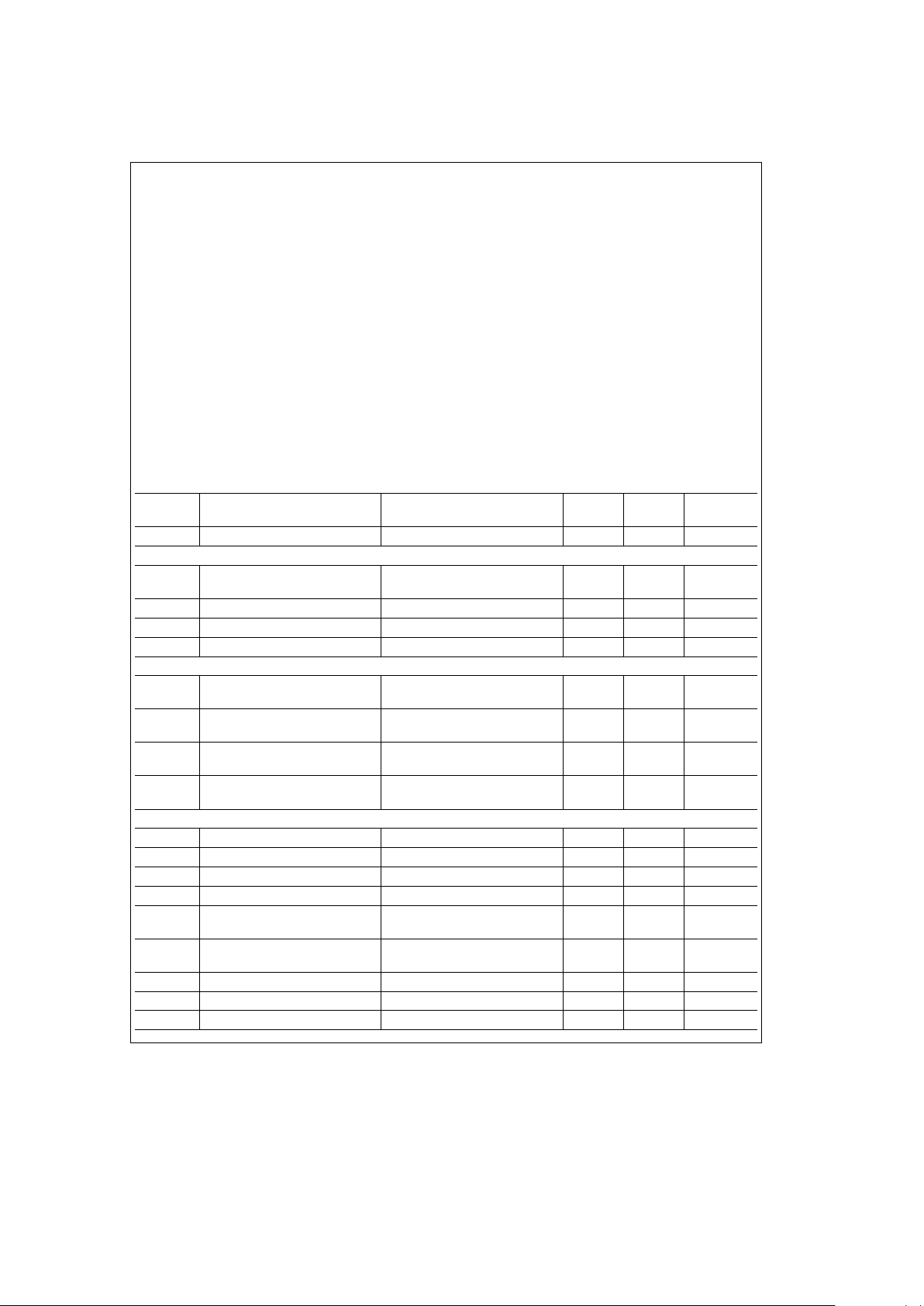
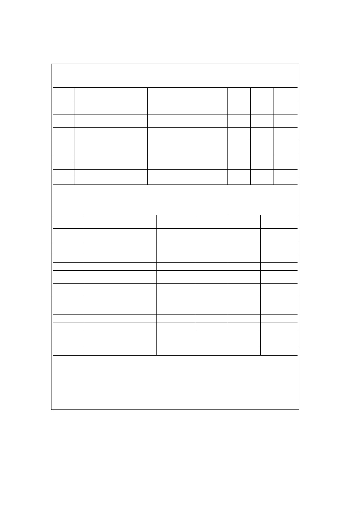
Converter Electrical Characteristics
The following specifications apply for V
M
a
e
V
A
a
e
V
D
a
e
5.0VDC,V
MID
e
V
A
a
/2e2.50V, V
REF
a
e
V
MID
a
1.25V,
V
REF
b
e
V
MID
b
1.25V, f
CLK
e
24.576 MHz, and dynamic tests are performed with an input signal magnitude set atb6dB
with respect to a full-scale input unless otherwise specified. Boldface limits apply for T
A
e
T
J
e
T
min
to T
max
; all other
limits T
A
e
T
J
e
25§C.
Symbol Parameter Conditions
Typical Limits Units
(Note 6) (Note 7) (Limit)
Resolution 16 Bits
f
CLK
e
24.576 MHz (f
s
e
192 kHz)
S/(NaD) Signal-to-NoiseaDistortion Ratio Measurement bandwidthe0.45f
s
76 72 dB (min)
f
IN
e
19 kHz
THD Total Harmonic Distortion f
IN
e
19 kHz 0.010 0.022 % (max)
IMD Intermodulation Distortion f
1
e
18.5 kHz, f
2
e
19.5 kHz 0.010 0.017 % (max)
Converter Noise Floor (Note 8) Measurement Bandwidthe0.45f
s
b
88
b
77 dBFS (min)
f
CLK
e
6.144 MHz (f
s
e
48 kHz)
S/(NaD) Signal-to-NoiseaDistortion Ratio Measurement bandwidthe0.45f
s
85
80 dB (min)
f
IN
e
5 kHz 73 dB (min)
THD Total Harmonic Distortion f
IN
e
5 kHz
0.002
0.0055 % (max)
0.008 % (max)
IMD Intermodulation Distortion f
1
e
4 kHz, f
2
e
5.5 kHz
0.003
0.009 % (max)
0.01 % (max)
Converter Noise Floor (Note 8) Measurement Bandwidthe0.45f
s
b
99
b
92 dBFS (min)
b
89 dBFS (min)
OTHER CONVERTER CHARACTERISTICS
Z
IN
Input Impedance (Note 9) 34 kX
DA
V
Gain Error
g
0.2
g
1.0 %FS (max)
V
OS
Input Offset Voltage 15 mV
I
A
Analog Power Supply Current 23 31 mA (max)
I
M
Modulator Power Supply Current f
CLK
e
24.576 MHz 1.6 2.4
mA (max)
f
CLK
e
6.144 MHz 0.4 0.8
I
D
Digital Power Supply Current f
CLK
e
24.576 MHz 50 65
mA (max)
f
CLK
e
6.144 MHz 13 23
I
SPD
Power-Down Supply Current I
A
a
I
D
a
I
M
0.25 1.3 mA
P
D
Power Dissipation 0.375 0.5 W
V
MID
V
A
a
/2 V
3
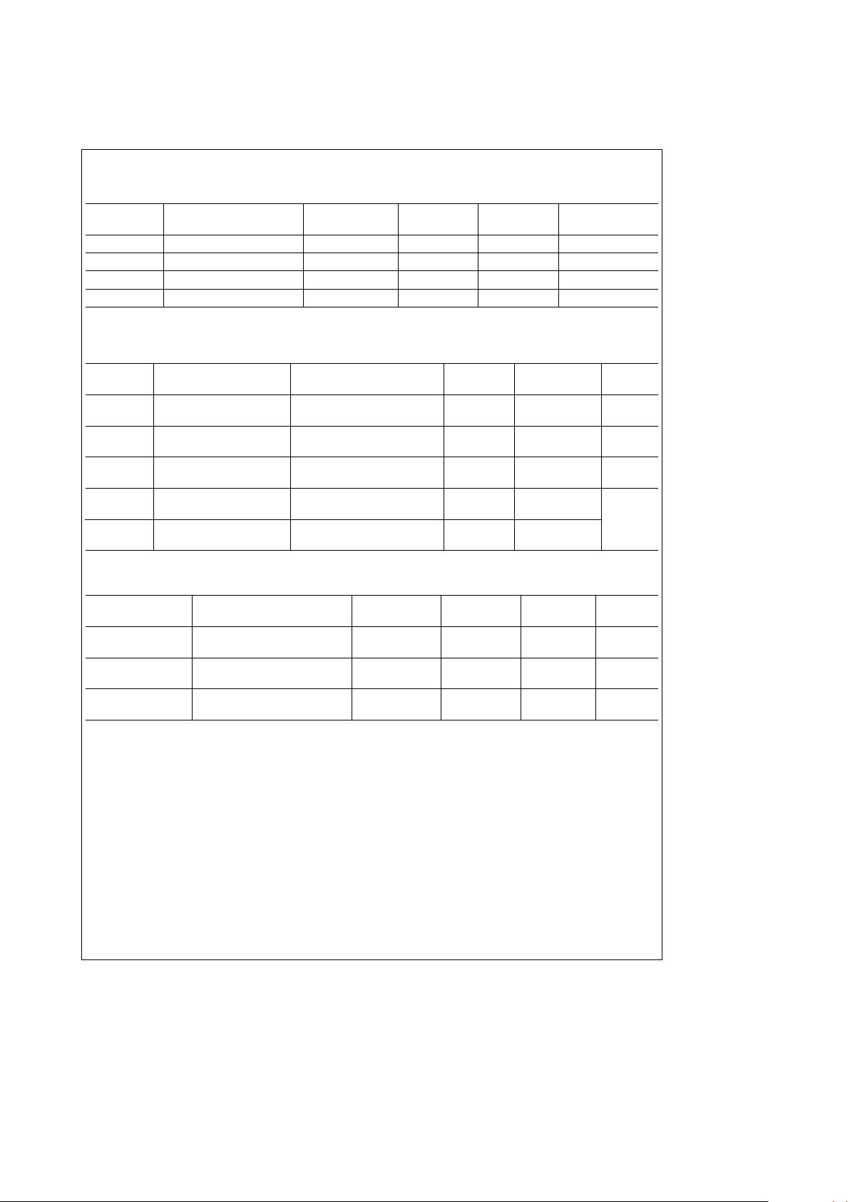
Digital Filter Characteristics
The following specifications apply for V
A
a
e
V
D
a
e
V
M
a
e
5V unless otherwise specified. Boldface limits apply for
T
A
e
T
J
e
T
min
to T
max
; all other limits T
A
e
T
J
e
25§C.
Symbol Parameter Conditions
Typical Limits Units
(Note 6) (Note 7) (Limit)
Stopband Rejection
b
90.0 dB
Passband Ripple
g
0.005 dB
3 dB Cutoff Frequency 0.45 fs
Data Latency 3,968 Clock Cycles
Reference Characteristics (ADC16471 Only)
The following specifications apply for V
A
a
e
V
D
a
e
V
M
a
e
5V, unless otherwise specified. Boldface limits apply for T
A
e
T
J
e
T
min
to T
max
; all other limits T
A
e
T
J
e
25§C.
Symbol Parameter Conditions
Typical Limits Units
(Note 6) (Note 7) (Limit)
V
REF
a
Positive Internal Reference
V
MID
a
1.25
V
MID
a
1.175 V (min)
Output Voltage V
MID
a
1.325 V (max)
V
REF
b
Negative Internal Reference
V
MID
b
1.25
V
MID
b
1.325 V (min)
Output Voltage V
MID
b
1.175 V (max)
D(V
REF
a
– Internal Reference
30 ppm/
§
C
V
REF
b
)/DT Temperature Coefficient
DV
REF
a
/DI Positive Internal Reference Sourcing (0 mAsI
s
a
10 mA)
3.4 6.0
Load Regulation Sinking (
b
1mAsIs0 mA)
mV (max)
DV
REF
b
/DI Negative Internal Reference Sinking (b1mAsIs0 mA)
3.2 6.0
Load Regulation Sourcing (0 mA
sIs
10 mA)
Input Reference Characteristics (ADC16071 Only)
The following specifications apply for V
A
a
e
V
D
a
e
V
M
a
e
5V.
Symbol Parameter Conditions
Typical Limits
Units
(Note 6) (Note 7)
V
REF
a
Positive Reference Voltage 1 V
V
A
a
V
V
REF
b
Negative Reference Voltage 0 V
V
A
ab
1V
V
REF
a
–V
REF
b
Total Reference Voltage 1 V
V
A
a
V
4
DC Electrical Characteristics
The following specifications apply for V
A
a
e
V
D
a
e
V
M
a
e
5V unless otherwise specified. Boldface limits apply for T
A
e
T
J
e
T
MIN
to T
MAX
; all other limits T
A
e
T
J
e
25§C.
Symbol Parameter Conditions
Typical Limits Units
(Note 6) (Note 7) (Limit)
V
IH
Logic High Input Voltage V
D
a
e
5.25V V
D
a
V (max)
2.3 V (min)
V
IL
Logic Low Input Voltage V
D
a
e
4.75V 0.8 V (max)
b
0.3 V (min)
V
OH
Logic High Output Voltage Logic High Output Currenteb400 mA,
2.4 V (min)
V
D
a
e
4.75V
V
OL
Logic Low Output Voltage Logic Low Output Currente2 mA,
0.5 V (max)
V
D
a
e
5.25V
I
IN(1)
Logical ‘‘1’’ Input Current 1.0 5.0 mA (max)
I
IN(0)
Logical ‘‘0’’ Input Current
b
1.0
b
5.0 mA (max)
I
TSI
SDO TRI-STATEÉLeakage Current V
IN
e
0.4V to 2.4V 1.0 5.0 mA (max)
C
IN
Logic Input Capacitance V
IN
e
0toV
D
a
5pF
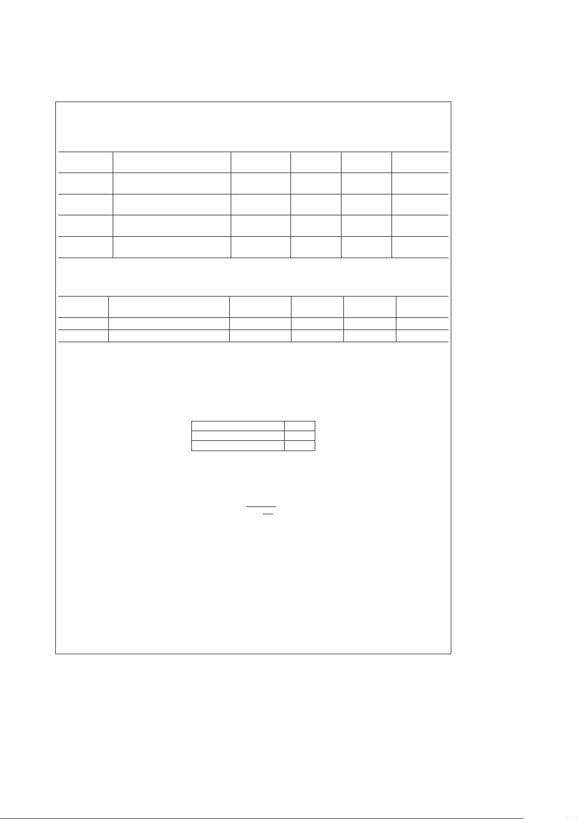
AC Electrical Characteristics for Clock In (CLK), Serial Clock Out (SCO), and
Frame Sync In (FSI)
The following specifications apply for V
A
a
e
V
D
a
e
V
M
a
e
5V unless otherwise specified. Boldface limits apply for T
A
e
T
J
e
T
MIN
to T
MAX
; all other limits T
A
e
T
J
e
25§C.
Symbol Parameter Conditions
Typical Limits Units
(Note 6) (Note 7) (Limit)
f
CLK
CLK Frequency Range 25 MHz (max)
(f
CLK
e
1/t
CLK
) 1 MHz (min)
t
CLK
CLK Period 1000 ns (max)
(t
CLK
e
1/f
CLK
) 40 ns (min)
t
CLKL
CLK Low Pulse Width 16 ns (min)
t
CLKH
CLK High Pulse Width 14 ns (min)
t
R
CLK Rise Time 10 ns (max)
3 ns (min)
t
F
CLK Fall Time 10 ns (max)
3 ns (min)
t
FSILOW
Minimum Frame Sync Input
2t
CLK
(min)Low Time before Frame Sync
Input Asserted High
t
FSISU
Frame Sync Input Setup Time 10 ns (min)
t
FSIH
Frame Sync Input Hold Time 10 ns (min)
t
SCOD
Serial Clock Output Delay
20 ns (max)
Time from Rising Edge
12
5 ns (min)
of CLK
t
SCO
Serial Clock Output Period 4 t
CLK
5
AC Electrical Characteristics for Frame Sync Out (FSO), Serial Clock Out
(SCO), and Serial Data Out (SDO)
The following specifications apply for V
A
a
e
V
D
a
e
V
M
a
e
5V unless otherwise specified. Boldface limits apply for T
A
e
T
J
e
T
MIN
to T
MAX
; all other limits T
A
e
T
J
e
25§C.
Symbol Parameter Conditions
Typical Limits Units
(Note 6) (Note 7) (Limit)
t
SCOFSOH
Delay from Serial Clock Out to
2 5 ns (max)
Frame Sync Output High
t
SCOFSOL
Delay from Serial Clock Out to
2 5 ns (max)
Frame Sync Output Low
t
SDOV
Delay from Serial Clock Out to
3 8 ns (max)
Serial Data Output Valid
t
FSIFSOL
Delay from Frame Sync Input to
8 t
CLK
(max)
Frame Sync Output Low
AC Electrical Characteristics for Data Output Enable (DOE)
The following specifications apply for V
A
a
e
V
D
a
e
V
M
a
e
5V unless otherwise specified. Boldface limits apply for T
A
e
T
J
e
T
MIN
to T
MAX
; all other limits T
A
e
T
J
e
25§C.
Symbol Parameter Conditions
Typical Limits Units
(Note 6) (Note 7) (Limit)
t
DOEE
Data Output Enable Delay Time 20 25 ns (max)
t
DOED
Data Output Disable Delay Time 16 20 ns (max)
Note 1: Absolute Maximum Ratings indicate limits beyond which damage to the device may occur. Operating Ratings indicate conditions for which the device is
functional, but do not guarantee specific performance limits. For guaranteed specifications and test conditions, see the Electrical Characteristics. The guaranteed
specifications apply for the test conditions listed. Some performance characteristics may degrade when the device is not operated under the listed test conditions.
Note 2: All voltages are measured with respect to GND, unless otherwise specified.
Note 3: When the input voltage (V
IN
) at any pin exceeds the power supply rails (V
IN
k
GND or V
IN
l
(V
A
a
,V
M
a
,orV
D
a
)), the current at that pin should be limited
to 25 mA. The 100 mA maximum package input current rating allows the voltage at any four pins, with an input current of 25 mA each, to simultaneously exceed the
power supply voltages.
Note 4: The maximum power dissipation is a function of the maximum junction temperature (T
J(MAX)
), total thermal resistance (iJA), and ambient temperature (TA).
The maximum allowable power dissipation at any ambient temperature is P
D(max)
e
(T
J(max)
b
TA)/iJA. When board mounted, the ADC16071/ADC16471’s
typical thermal resistance is:
Order Number i
JA
ADC16071CIN, ADC16471CIN 47§C/W
ADC16071CIWM, ADC16471CIWM 72§C/W
Note 5: Human body model, 100 pF discharge through a 1.5 kX resistor. The machine model is a 200 pF capacitor discharged directly into each pin.
Note 6: Typicals are at T
A
e
25§C and represent most likely parametric norm.
Note 7: Limits are guaranteed to National’s AOQL (Average Output Quality Level).
Note 8: The V
IN
a
pin is shorted to the V
IN
b
pin.
Note 9: The input impedance between V
IN
a
and V
IN
b
due to the effective resistance of the switch capacitor input varies as follows:
Z
IN
e
10
12
2.35* (
f
CLK
2
)
6
 Loading...