NSC ADC14071CIVBH Datasheet
ADC14071
14-Bit, 7 MSPS, 380 mW A/D Converter
ADC14071 14-Bit, 7 MSPS, 380 mW A/D converter
November 1999
General Description
The ADC14071 is a 14-bit, monotholic analog to digital converter capable of conversion rates up to 8 Megasamples per
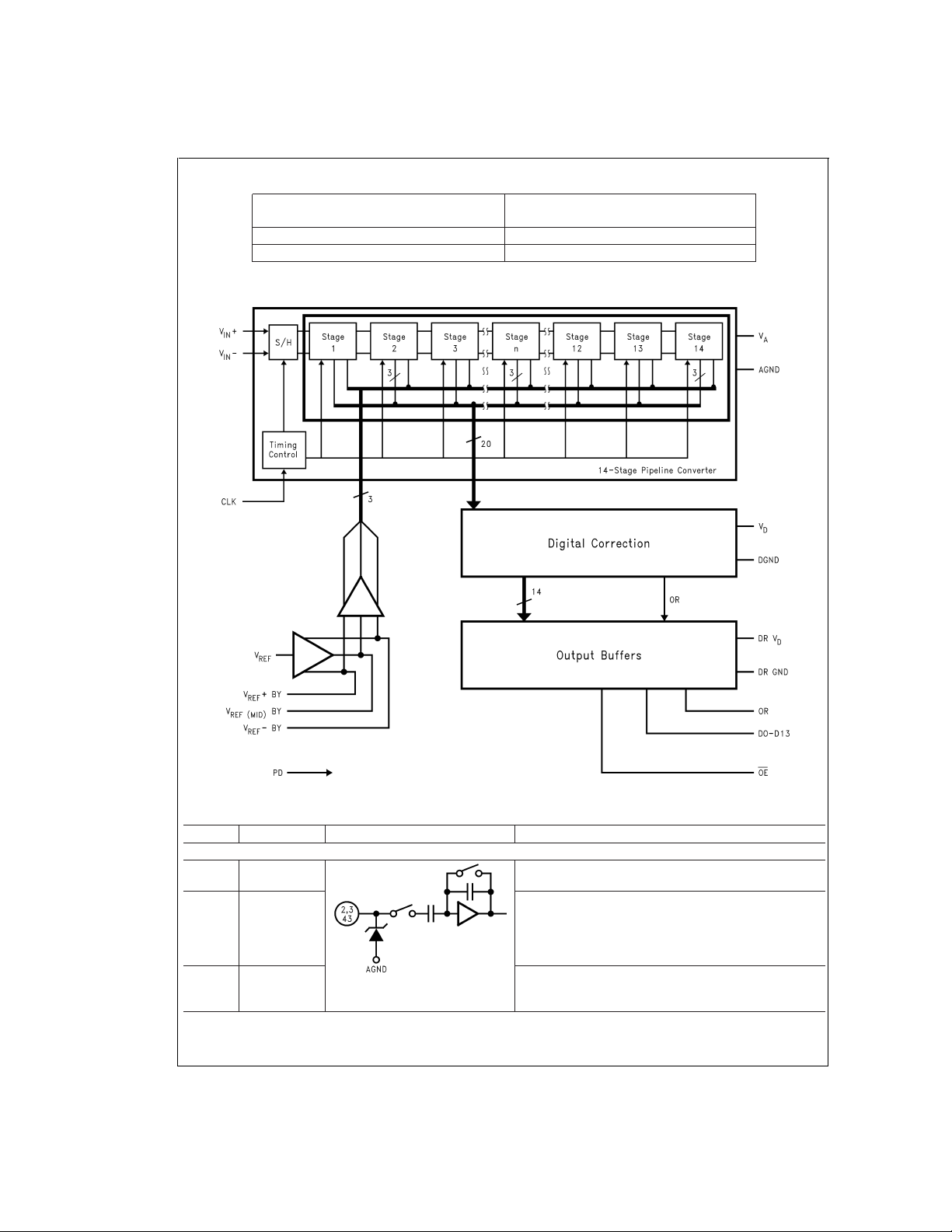
second. This CMOS converter uses a differential, piperlined
architecture with digital error correction and an on-chip
track-and-hold circuit to maintain superb dynamic performance with input frequenciesupto20MHz.Tested and guaranteed dynamic performance specifications provide the designer with known performance. TheADC14071operateson
a +5V single supply consuming just 380mW (typical). The
Power Down feature reduces power consumption to 20mW,
typical.
The differential inputs provide a full scale input swing of
±
V
with the possibilityofasingleinput.Fulluse of the dif-
REF
ferential input is recommended for optimum perfomance. For
ease of use, the reference input is single ended. This singleended reference input is converted on-chip to a differential
reference configuration for use by the processing circuitry.
Output data format is 14-bit straight binary.
The ADC14071 may be used to replace many hybrid converters with a resultant saving of space, power and cost.
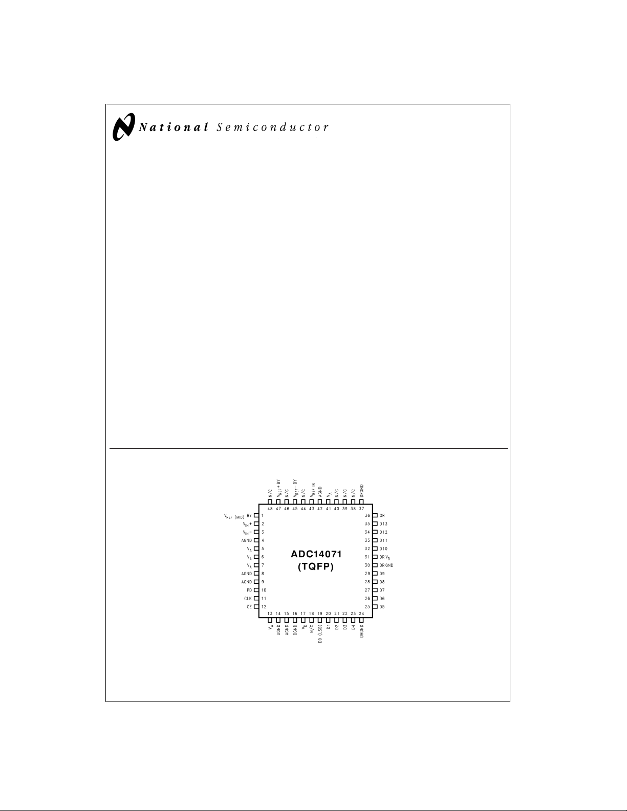
The ADC14071 comes in a 48-pin TQFP and is specified to
operate over the industrial temperature range of −40˚C to
+85˚C.
Connection Diagram
Features
n Single +5V Operation
n Power Down Mode
n TTL/CMOS Input/Output Compatible
Key Specifications
n Resolution 14 Bits
n Max Conversion Rate 7 Msps (min)
n DNL
n SNR (f
n ENOB (f
n Supply Voltage +5V
n Power Consumption 380 mW (typ)
=
500 kHz) 80 dB (typ)
IN
= 500 kHz) 12.6 Bits (typ)
W
±
0.6 LSB (typ)
±
5
Applications
n Document Scanners
n Imaging
n Instrumentation
n PC-Based Data Acquisition
n Spectrum Analyzers
n Sonar/Radar
n xDSL
n Wireless Local Loop
n Data Acquisition Systems
n DSP Front End
%
DS101101-1
TRI-STATE®is a registered trademark of National Semiconductor Corporation.
© 1999 National Semiconductor Corporation DS101101 www.national.com
Ordering Information
ADC14071
Block Diagram
Industrial Temperature Range
(−40˚C ≤ T
≤ +85˚C)
A
NS Package
ADC14071CIVBH VBH48A 48-Pin Thin Quad Flatpak
ADC14071EVAL Evaluation System
Pin Descriptions and Equivalent Circuits
Pin No. Symbol Equivalent Circuit Description
ANALOG I/O
2V
3V
43 V
www.national.com 2
IN
IN
REF IN
+
−
Non-Inverting analog signal input. With a 2.0V reference
voltage the input signal voltage range is from 0V to 2.0V.
Inverting analog signal input. With a 2.0V reference voltage
the input signal voltage range is from 0V to 2.0V. This pin
may be connected to a voltage of
for single-ended operation, but a balanced input signal is
required for best performance.
Positive reference input. This pin should be bypassed to
AGND with a 0.1 µF monolithic capacitor. V
nominal and should be in the range of 1.0V to 2.7V.
DS101101-2
1
⁄2the reference voltage
is 2.0V
REF
Pin Descriptions and Equivalent Circuits (Continued)
Pin No. Symbol Equivalent Circuit Description
ANALOG I/O
ADC14071
47 V
1V
REF (MID)
45 V
DIGITAL I/O
11 CLOCK
12 OE
10 PD
REF
REF
+BY
−BY
BY
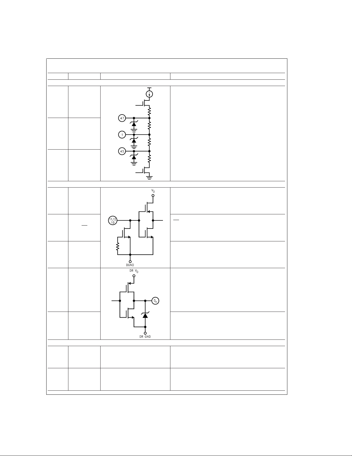
These pins are high impedance reference bypass pins only.
Connect a 0.1µF capacitor from each of these pins the
AGND. DO NOT connect anything else to these pins.
Digital clock input. The range of frequencies for this input is
25 kHz to 8 MHz (typical) with guaranteed performance at 7
MHz. The input is sampled on the rising edge of this input.
OE is the output enable pin that, when low, enables the
TRI-STATE®data output pins. When this pin is high, the
outputs are in a high impedance state.
PD is the Power Down input pin. When high, this input puts
the converter into the power down mode. When this pin is
low, the converter is in the active mode.
36 OR
19-23,
25-29,
D0–D13
32-35
ANALOG POWER
5, 6, 7,
13, 41
4, 8, 9,
14, 15,
AGND
42
Out of Range pin. A high at this output pin indicates that the
input voltage is either above the reference voltage or is
below ground. When this pin is high, the digital output pins
will indicate a full scale for input voltages above the
reference voltage, or will indicate a zero scale for input
voltages below zero scale.
Digital data output pins that make up the 14-bit conversion
results. D0 is the LSB, while D13 is the MSB of the straight
binary output word.
Positive analog supply pins. These pins should be
V
A
connected to a clean, quiet +5V voltage source and
bypassed to AGND with 0.1 µF monolithic capacitors located
within 1 cm of these power pins, and by a 10 µF capacitor.
The ground return for the analog supply. AGND and DGND
should be connected together directly beneath the
ADC14071 package. See Section 5 (Layout and Grounding)
for more details.
www.national.com3

Pin Descriptions and Equivalent Circuits (Continued)
Pin No. Symbol Equivalent Circuit Description
ADC14071
DIGITAL POWER
Positive digital supply pin. This pin should be connected to
17 V
16 DGND
31 DR V
24, 30,
37
NC
18, 38,
39, 40,
44, 46,
48
D
D
DR GND
NC
the same clean, quiet +5V source as is V
DGND with a 0.1 µF monolithic capacitor in parallel with a
10 µF capacitor, both located within 1 cm of the power pin.
The ground return for the digital supply. AGND and DGND
should be connected together directly beneath the
ADC14071 package. See Section 5 (Layout and Grounding)
for more details.
Positive digital supply pin for the ADC14071’s output drivers.
This pin should be connected to a voltage source of +3 to
+5V and bypassed to DR GND with a 0.1 µF monolithic
capacitor. If the supply for this pin is different from the
supply used for V
a 10 µF tantalum capacitor and never exceed the voltage on
. All bypass capacitors should be located within 1 cm of
V
D
the supply pin.
and VD, it should also be bypassed with
A
The ground return for the digital supply for the ADC14071’s
output drivers. These pins should be connected to the
system digital ground, but not be connected in close
proximity to the ADC14071’s DGND or AGND pins. See
Section 5 (Layout and Grounding) for more details.
All pins marked NC (no connect) should not be connected to
any potential (or to ground). Allow these pins to float.
and bypassed to
A
www.national.com 4
Absolute Maximum Ratings (Notes 1, 2)
If Military/Aerospace specified devices are required,
please contact the National Semiconductor Sales Office/
Distributors for availability and specifications.
Supply Voltage
+
=
=
(V
−DRVD,VD−DRV
V
A
Voltage on Any I/O Pin −0.5V to V
Input Current at Pins 1, 45 and
47(Note 3)
Input Current at Any Other Pin (Note
3)
Package Input Current (Note 3)
Power Dissipation at T
ESD Susceptibility (Note 5)
Human Body Model
Machine Model
=
V
V
A
D
) 6.0V
DR V
D
D
=
25˚C See (Note 4)
A
+
+0.5V
±
10 mA
±
25 mA
±
50 mA
1500V
≥0V
200V
Soldering Temperature, Infrared,
10 seconds (Note 6) 300˚C
Storage Temperature −65˚C to +150˚C
Operating Ratings (Notes 1, 2)
Operating Temperature Range −40˚C ≤ T
V
A,VD
DR V
V
REF
D
+4.75V to +5.25V
Digital Inputs −0.3V to V
Analog Inputs −0.3V to V
| ≤100 mV
|V
A−VD
|AGND − DGND| 0V to 100 mV
≤ +85˚C
A
2.7V to V
1.0V to 2.7V
+ 0.3V
D
+ 0.3V
A
ADC14071
D
Converter Electrical Characteristics
=
The following specifications apply for AGND=DGND=DR GND=0V, V
=
V
REF IN
apply for T
+2.0V, V
=
A
(common mode)=1.0V, f
IN
=
T
to T
T
J
MIN
MAX
: all other limits T
CLK
=
A
@
7 MHz
=
=
T
25˚C (Notes 7, 8, 9)
J
50%duty cycle, tr,t
Symbol Parameter Conditions
=
V
A
+5.0V
D
r
=
DC
4ns, C
(Note 10)
Typical
STATIC CONVERTER CHARACTERISTICS
Resolution with No Missing Codes 14 Bits (min)
INL Integral Non-Linearity (note 12)
DNL Differential Non-Linearity
Positive and Negative Full-Scale
FSE
Error
25˚C 0.9 2.3
TC FSE Full-Scale Error Tempco −5 ppm/˚C
ZSE Zero Offset Error 25˚C 0.1
TC ZSE Zero Offset Error Tempco −0.6 ppm/˚C
REFERENCE AND ANALOG INPUT CHARACTERISTICS
V
Reference Voltage Range 2.00
REF
Reference Input Resistance 10M Ohms
R
R
C
Reference Input Capacitance 5 pF
R
+
Input Voltage Range (V
V
IN
C
IN
+
V
IN
−
,V
Input Capacitance V
IN
−
−V
)VIN(common Mode) = V
IN
IN
IN
=
1.0V+0.7 Vrms
/2
REF
(CLK LOW) 14 pF
(CLK HIGH) 5 pF
DYNAMIC CONVERTER CHARACTERISTICS
BW Full Power Bandwidth
ENOB Effective Number of Bits
SINAD Signal-to-Noise and Distortion
SNR Signal -to-Noise Ratio (Note 13)
THD Total Harmonic Distortion
−1 dB 20 MHz
−3 dB 25 MHz
=
f
500 kHz 12.6 12.0 Bits (min)
IN
=
f
3.5 MHz 12.0 Bits
IN
=
f
500 kHz 77 74 dB (min)
IN
=
f
3.5 MHz 74 dB
IN
=
f
500 kHz 80 78 dB (min)
IN
=
f
3.5 MHz 77 dB
IN
=
f
500 kHz −83 −76 dB (min)
IN
=
f
3.5 MHz −79 dB
IN
=
,DRV
L
±
2.2 LSB
±
0.6
3.0V or 5.0V, PD=0V,
D
=
20 pF/pin. Boldface limits
Limits
(Note 11)
+1.0
−0.85
LSB (max)
1.0
2.7
±
±
2.0
1.0
±
2.7
V(max)
V(max)
Units
%
FS
%
FS
V(min)
V(min)
www.national.com5
Converter Electrical Characteristics (Continued)
The following specifications apply for AGND=DGND=DR GND=0V, V
V
REF IN
ADC14071
apply for T
=
+2.0V, V
(common mode)=1.0V, f
IN
=
=
T
A
T
J
MIN
to T
MAX
: all other limits T
Symbol Parameter Conditions
DYNAMIC CONVERTER CHARACTERISTICS
SFDR Spurious Free Dynamic Range
IMD Intermodulation Distortion
CLK
=
f
IN
f
IN
f
IN1
f
IN2
@
7 MHz
=
=
T
25˚C (Notes 7, 8, 9)
A
J
=
500 kHz 90 dB
=
3.5 MHz 81 dB
=
95 kHz
=
105 kHz
=
V
A
50%duty cycle, tr,t
D
=
r
+5.0V
=
4ns, C
DC
L
Typical
(Note 10)
3.0V or 5.0V, PD=0V,
D
=
20 pF/pin. Boldface limits
Limits
(Note 11)
=
,DRV
−97 dB
Units
DC and Logic Electrical Characteristics
The following specifications apply for AGND=DGND=DR GND=0V, V
V
REF IN
ply for T
=
+2.0V, V
A
(common mode)=1.0V, f
IN
=
=
T
to T
T
J
MIN
: all other limits T
MAX
Symbol Parameter Conditions
CLOCK OE, PD DIGITAL INPUT CHARACTERISTICS
V
Logical “1” Input Voltage V
IH
V
Logical “0” Input Voltage V
IL
I
Logical “1” Input Current V
IH
I
Logical “0” Input Current V
IL
C
VINInput Capacitance 5 pF
IN
D00 – D13 DIGITAL OUTPUT CHARACTERISTICS
V
Logical “1” Output Voltage
OH
Logical “0” Output Voltage
V
OL
TRI-STATE Output Current
I
OZ
Output Short Circuit Source
+I
SC
Current
Output Short Circuit Sink
−I
SC
Current
POWER SUPPLY CHARACTERISTICS
Analog Supply Current PD=DGND 75.7 81 mA(max)
I
A
I
D+IDR
Digital Supply Current PD=DGND, no output load, dc input 0.3 2 mA(max)
Total Power Consumption
PSRR
Power Supply Rejection
Ratio
=
CLK
=
A
+
=
5.25V 2.0 V(min)
+
=
5.25V 0.8 V(max)
=
5.0V 1 µA
IN
=
0V −1 µA
IN
=
DR V
D
=
DR V
D
=
DR V
D
=
DR V
D
=
V
3V or 5V 100 nA
OUT
=
V
0V −100 nA
OUT
=
DR V
D
=
V
DR V
OUT
@
7 MHz
T
4.75V, I
2.7V, I
4.75V, I
2.7V, I
3V, V
50%duty cycle, tr,t
=
25˚C (Notes 7, 8, 9)
J
=
−360 µA 4.5 V(min)
OUT
=
−360 µA 2.5 V(min)
OUT
=
1.6 mA 0.4 V(max)
OUT
=
1.6 mA 0.4 V(max)
OUT
=
0V −10 mA
OUT
=
3V 12 mA
D
PD=DGND, no output load, dc input 380 425 mW(max)
PD=DR V
, no output load, dc input 20 mW
D
Change in FS Error with 0.5V change in V
250 mV
100 kHz riding on V
PP
=
=
V
A
A
+5.0V
D
r
=
A
DC
4ns, C
=
,DRV
L
3.0V or 5.0V, PD=0V,
D
=
20 pF/pin. Boldface limits ap-
Typical
(Note
10)
Limits
(Note
11)
70 dB
46 dB
Units
AC Electrical Characteristics
The following specifications apply for AGND=DGND=DR GND=0V, V
=
V
REF IN
apply for T
+2.0V, V
=
A
(common mode)=1.0V, f
IN
=
to T
T
T
J
MIN
: all other limits T
MAX
CLK
=
A
@
7 MHz
50%duty cycle, tr,t
=
=
T
25˚C (Notes 7, 8, 9)
J
Symbol Parameter Conditions
f
CLK
Conversion Clock Frequency
Conversion Clock Duty Cycle
www.national.com 6
=
A
=
V
+5.0V
D
=
f
DC
4 ns, C
(Note 10)
=
,DRV
L
Typical
3.0V or 5.0V, PD=0V,
D
=
20 pF/pin. Boldface limits
Limits
(Note 11)
25
8 7
45
55
Units
kHz(min)
MHz(max)
%
(min)
%
(max)
 Loading...