NSC ADC12C170HFEB, ADC12C170 Datasheet
February 2007
ADC12C170
12-Bit, 170 MSPS, 1.1 GHz Bandwidth A/D Converter with
CMOS outputs
General Description
The ADC12C170 is a high-performance CMOS analog-todigital converter capable of converting analog input signals
into 12-Bit digital words at rates up to 170 Mega Samples Per
Second (MSPS). This converter uses a differential, pipelined
architecture with digital error correction and an on-chip sample-and-hold circuit to minimize power consumption and the
external component count, while providing excellent dynamic
performance. A unique sample-and-hold stage yields a fullpower bandwidth of 1.1 GHz. The ADC12C170 operates from
dual +3.3V and +1.8V power supplies and consumes 715 mW
of power at 170 MSPS.
The separate +1.8V supply for the digital output interface allows lower power operation with reduced noise. A powerdown feature reduces the power consumption to 5 mW while
still allowing fast wake-up time to full operation. In addition
there is a sleep feature which consumes 50 mW of power and
has a faster wake-up time.
The differential inputs provide a full scale differential input
swing equal to 2 times the reference voltage. A stable 1.0V
internal voltage reference is provided, or the ADC12C170 can
be operated with an external reference.
Clock mode (differential versus single-ended) and output data
format (offset binary versus 2's complement) are pin-selectable. A duty cycle stabilizer maintains performance over
a wide range of input clock duty cycles.
The ADC12C170 is pin compatible with the ADC14155.
It is available in a 48-lead LLP package and operates over the
industrial temperature range of −40°C to +85°C.
Features
■
1.1 GHz Full Power Bandwidth
■
Internal sample-and-hold circuit
■
Low power consumption
■
Internal precision 1.0V reference
■
Single-ended or Differential clock modes
■
Clock Duty Cycle Stabilizer
■
Dual +3.3V and +1.8V supply operation (+/- 10%)
■
Power-down and Sleep modes
■
Offset binary or 2's complement output data format
■
Pin-compatible with: ADC14155
■
48-pin LLP package, (7x7x0.8mm, 0.5mm pin-pitch)
Key Specifications
■
Resolution 12 Bits
■
Conversion Rate 170 MSPS
■
SNR (fIN = 70 MHz) 67.2 dBFS (typ)
■
SFDR (fIN = 70 MHz) 85.4 dBFS (typ)
■
ENOB (fIN = 70 MHz) 10.8 bits (typ)
■
Full Power Bandwidth 1.1 GHz (typ)
■
Power Consumption 715 mW (typ)
Applications
■
High IF Sampling Receivers
■
Wireless Base Station Receivers
■
Power Amplifier Linearization
■
Multi-carrier, Multi-mode Receivers
■
Test and Measurement Equipment
■
Communications Instrumentation
■
Radar Systems
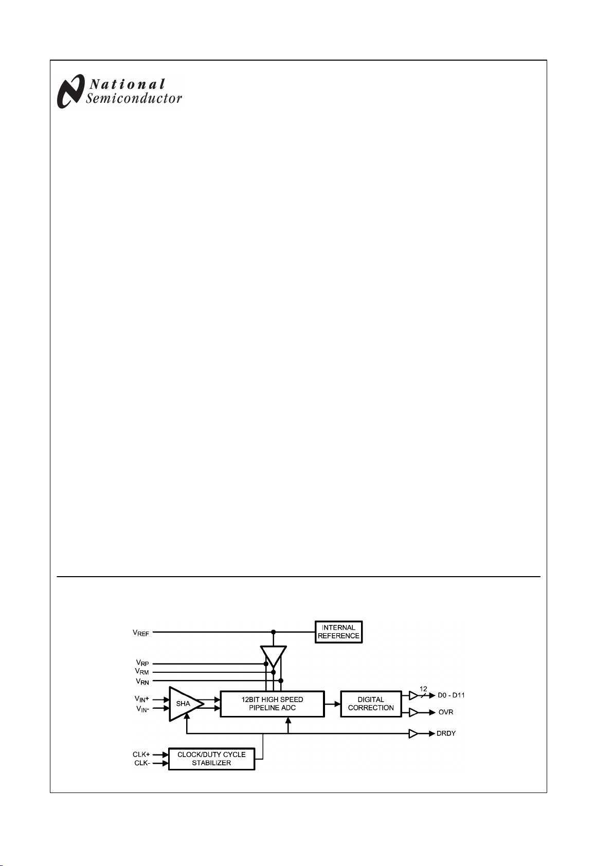
Block Diagram
20209202
© 2007 National Semiconductor Corporation 202092 www.national.com
ADC12C170 12-Bit, 170 MSPS, 1.1 GHz Bandwidth A/D Converter
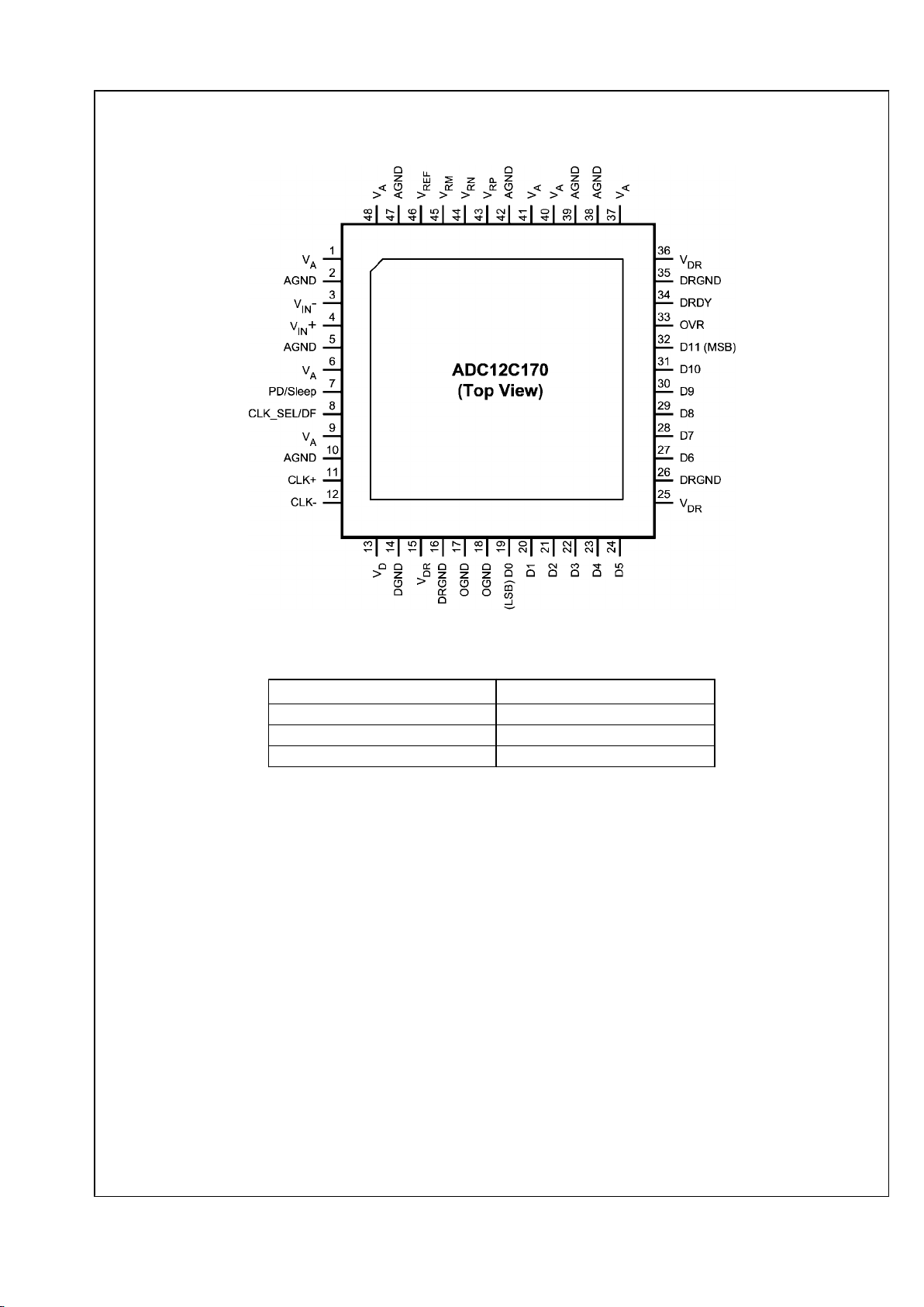
Connection Diagram
20209201
Ordering Information
Industrial (−40°C ≤ TA ≤ +85°C)
Package
ADC12C170CISQ 48 Pin LLP
ADC12C170LFEB Evaluation Board
ADC12C170HFEB Evaluation Board
www.national.com 2
ADC12C170
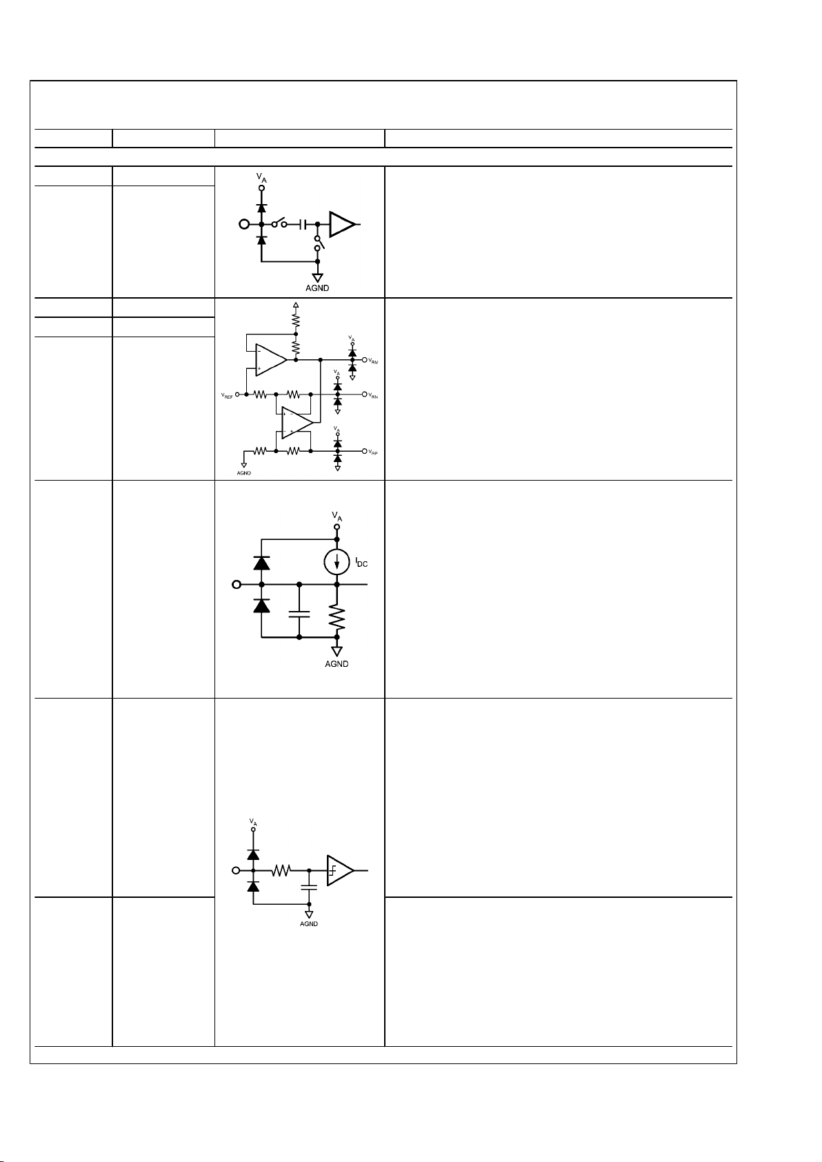
Pin Descriptions and Equivalent Circuits
Pin No. Symbol Equivalent Circuit Description
ANALOG I/O
3
VIN− Differential analog input pins. The differential full-scale input signal
level is two times the reference voltage with each input pin signal
centered on a common mode voltage, VCM.
4
VIN+
43
V
RP
These pins should each be bypassed to AGND with a low ESL
(equivalent series inductance) 0.1 µF capacitor placed very close
to the pin to minimize stray inductance. A 0.1 µF capacitor should
be placed between VRP and VRN as close to the pins as possible,
and a 10 µF capacitor should be placed in parallel.
VRP and VRN should not be loaded. VRM may be loaded to 1mA for
use as a temperature stable 1.5V reference.
It is recommended to use VRM to provide the common mode
voltage, VCM, for the differential analog inputs, VIN+ and VIN−.
45
V
RM
44
V
RN
46
V
REF
This pin can be used as either the +1.0V internal reference voltage
output (internal reference operation) or as the external reference
voltage input (external reference operation).
To use the internal reference, V
REF
should be decoupled to AGND
with a 0.1 µF, low equivalent series inductance (ESL) capacitor. In
this mode, V
REF
defaults as the output for the internal 1.0V
reference.
To use an external reference, overdrive this pin with a low noise
external reference voltage. The input impedance looking into this
pin is 9kΩ. Therefore, to overdrive this pin, the output impedance
of the external reference source should be << 9kΩ.
This pin should not be used to source or sink current.
The full scale differential input voltage range is 2 * V
REF
.
8 CLK_SEL/DF
This is a four-state pin controlling the input clock mode and output
data format.
CLK_SEL/DF = VA, CLK+ and CLK− are configured as a
differential clock input. The output data format is 2's complement.
CLK_SEL/DF = (2/3)*VA, CLK+ and CLK− are configured as a
differential clock input. The output data format is offset binary.
CLK_SEL/DF = (1/3)*VA, CLK+ is configured as a single-ended
clock input and CLK− should be tied to AGND. The output data
format is 2's complement.
CLK_SEL/DF = AGND, CLK+ is configured as a single-ended clock
input and CLK− should be tied to AGND. The output data format is
offset binary.
7 PD/Sleep
This is a three-state input controlling Power Down and Sleep
modes.
PD = VA, Power Down is enabled. In the Power Down state only
the reference voltage circuitry remains active and power
dissipation is reduced.
PD = VA/2, Sleep mode is enabled. Sleep mode is similar to Power
Down mode - it consumes more power but has a faster recovery
time.
PD = AGND, Normal operation.
3 www.national.com
ADC12C170
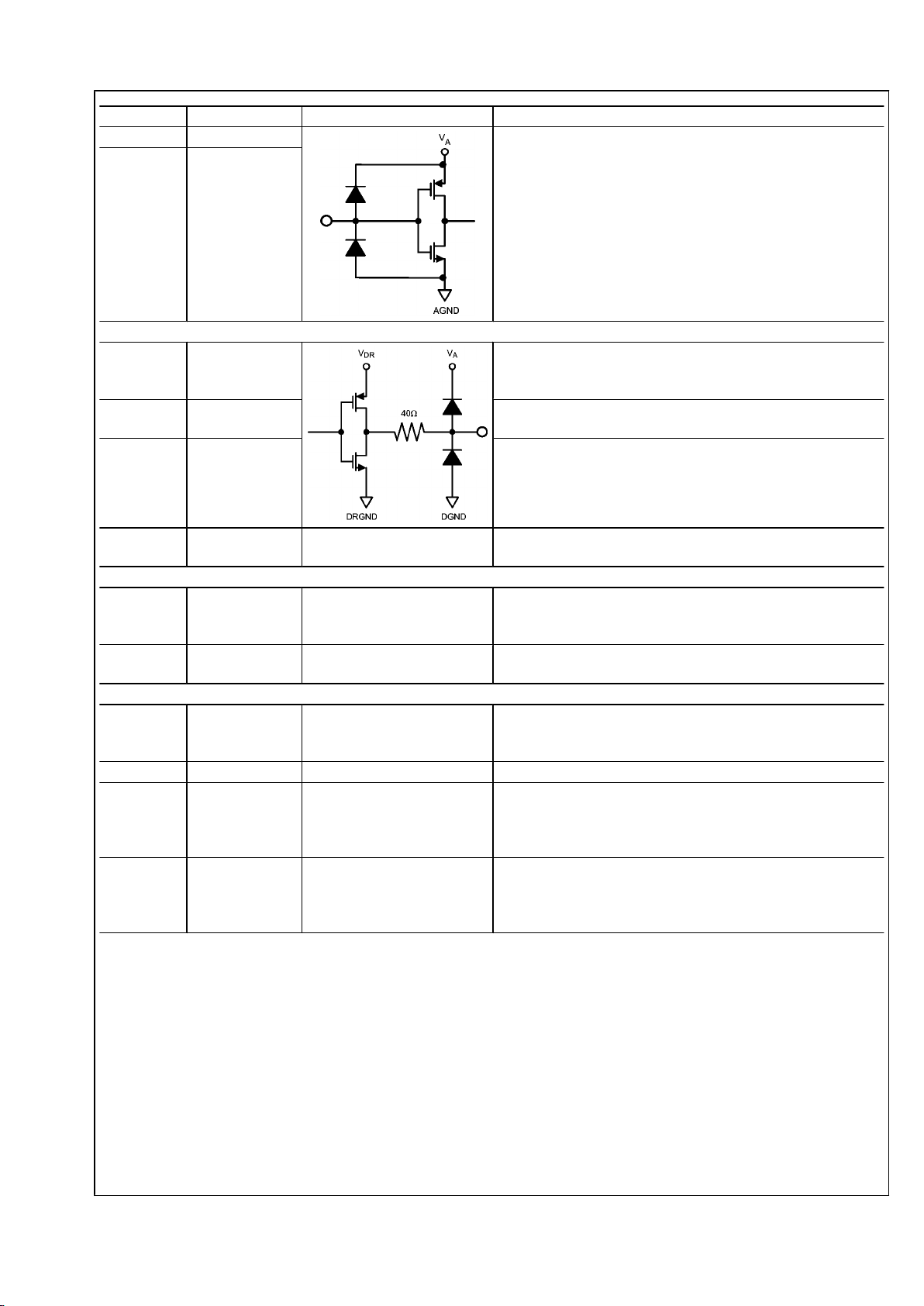
Pin No. Symbol Equivalent Circuit Description
11 CLK+ The clock input pins can be configured to accept either a single-
ended or a differential clock input signal.
When the single-ended clock mode is selected through CLK_SEL/
DF (pin 8), connect the clock input signal to the CLK+ pin and
connect the CLK− pin to AGND.
When the differential clock mode is selected through CLK_SEL/DF
(pin 8), connect the positive and negative clock inputs to the CLK
+ and CLK− pins, respectively.
The analog input is sampled on the falling edge of the clock input.
12 CLK−
DIGITAL I/O
19-24,
27-32
D0–D11
Digital data output pins that make up the 12-Bit conversion result.
D0 (pin 19) is the LSB, while D11 (pin 32) is the MSB of the output
word. Output levels are CMOS compatible.
33 OVR
Over-Range Indicator. This output is set HIGH when the input
amplitude exceeds the 12-Bit conversion range (0 to 4095).
34 DRDY
Data Ready Strobe. This pin is used to clock the output data. It has
the same frequency as the sampling clock. One word of data is
output in each cycle of this signal. The rising edge of this signal
should be used to capture the output data.
17-18 OGND
Output GND, internally tied to GND through 5k ohm resistor to
provide pin compatibility with 14 bit ADCs.
ANALOG POWER
1, 6, 9, 37, 40,
41, 48
V
A
Positive analog supply pins. These pins should be connected to a
quiet +3.3V source and be bypassed to AGND with 0.01 µF and
0.1 µF capacitors located close to the power pins.
2, 5, 10, 38,
39, 42, 47
AGND The ground return for the analog supply.
DIGITAL POWER
13
V
D
Positive digital supply pin. This pin should be connected to a quiet
+3.3V source and be bypassed to DGND with a 0.01 µF and 0.1
µF capacitor located close to the power pin.
14 DGND The ground return for the digital supply.
15, 25, 36
V
DR
Positive driver supply pin for the output drivers. This pin should be
connected to a quiet voltage source of +1.8V and be bypassed to
DRGND with 0.01 µF and 0.1 µF capacitors located close to the
power pins.
16, 26, 35 DRGND
The ground return for the digital output driver supply. These pins
should be connected to the system digital ground, but not be
connected in close proximity to the ADC's DGND or AGND pins.
See Section 6.0 (Layout and Grounding) for more details.
www.national.com 4
ADC12C170

Absolute Maximum Ratings
(Notes 1, 2)
If Military/Aerospace specified devices are required,
please contact the National Semiconductor Sales Office/
Distributors for availability and specifications.
Supply Voltage (VA, VD) −0.3V to 4.2V
Supply Voltage (VDR) −0.3V to 2.35V
|VA–VD|
≤ 100 mV
Voltage on Any Input Pin
(Not to exceed 4.2V)
−0.3V to (VA +0.3V)
Voltage on Any Output Pin
(Not to exceed 2.35V)
-0.3V to (VDR +0.2V)
Input Current at Any Pin other
than Supply Pins (Note 3)
±5 mA
Package Input Current (Note 3) ±50 mA
Max Junction Temp (TJ) +150°C
Thermal Resistance (θJA)
24°C/W
Package Dissipation at TA = 25°
C (Note 4)
5.2W
ESD Rating
Human Body Model (Note 5) 2000 V
Machine Model (Note 5) 200 V
Charge Device Model 1000 V
Storage Temperature −65°C to +150°C
Soldering process must comply with National
Semiconductor's Reflow Temperature Profile
specifications. Refer to www.national.com/packaging.
(Note 6)
Operating Ratings (Notes 1, 2)
Operating Temperature
−40°C ≤ TA ≤ +85°C
Supply Voltage (VA, VD) +3.0V to +3.6V
Output Driver Supply (VDR)
+1.6V to +2.0V
CLK −0.05V to (VA + 0.05V)
Clock Duty Cycle 30/70 %
Analog Input Pins 0V to 2.6V
V
CM
1.4V to 1.6V
|AGND-DGND|
≤100mV
5 www.national.com
ADC12C170
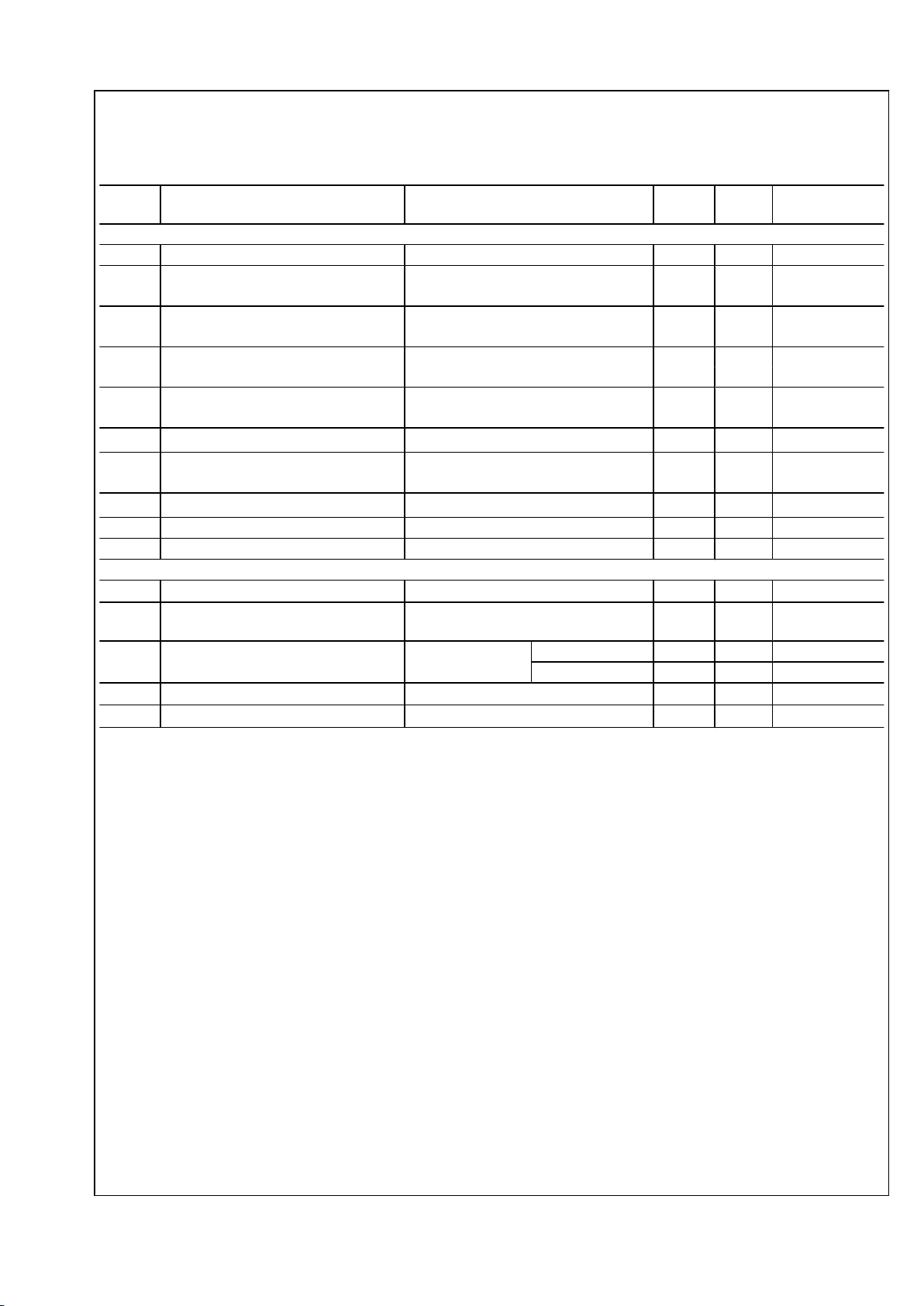
Converter Electrical Characteristics
Unless otherwise specified, the following specifications apply: VIN = -1dBFS, AGND = DGND = DRGND = 0V, VA = VD = +3.3V,
VDR = +1.8V, Internal V
REF
= +1.0V, f
CLK
= 170 MHz, VCM = VRM, CL = 5 pF/pin, Single-Ended Clock Mode, Offset Binary Format.
Typical values are for TA = 25°C. Boldface limits apply for T
MIN
≤ TA ≤ T
MAX
. All other limits apply for TA = 25°C (Notes 7, 8, 9)
Symbol Parameter Conditions
Typical
(Note 10)
Limits
Units
(Limits)
STATIC CONVERTER CHARACTERISTICS
Resolution with No Missing Codes 12 Bits (min)
INL Integral Non Linearity (Note 11)
±0.85
2.95 LSB (max)
-3.29 LSB (min)
DNL Differential Non Linearity
±0.54
1.3 LSB (max)
-0.92 LSB (min)
PGE Positive Gain Error +0.85
3.38 %FS (max)
-2.10 %FS (min)
NGE Negative Gain Error -0.31
3.00 %FS (max)
-3.57 %FS (min)
TC GE Gain Error Tempco
−40°C ≤ TA ≤ +85°C
+8.0 ppm/°C
V
OFF
Offset Error (VIN+ = VIN−)
−0.13
0.89 %FS (max)
-1.14 %FS (min)
TC V
OFF
Offset Error Tempco
−40°C ≤ TA ≤ +85°C
+0.5 ppm/°C
Under Range Output Code 0 0
Over Range Output Code 4095 4095
REFERENCE AND ANALOG INPUT CHARACTERISTICS
V
CM
Common Mode Input Voltage 1.5 V
V
RM
Reference Ladder Midpoint Output
Voltage
Output load = 1 mA 1.5 V
C
IN
VIN Input Capacitance (each pin to GND)
(Note 12)
VIN = 1.5 Vdc
± 0.5 V
(CLK LOW) 9 pF
(CLK HIGH) 6 pF
V
REF
Reference Voltage (Note 13) 1.00 V
Reference Input Resistance 9
kΩ
www.national.com 6
ADC12C170
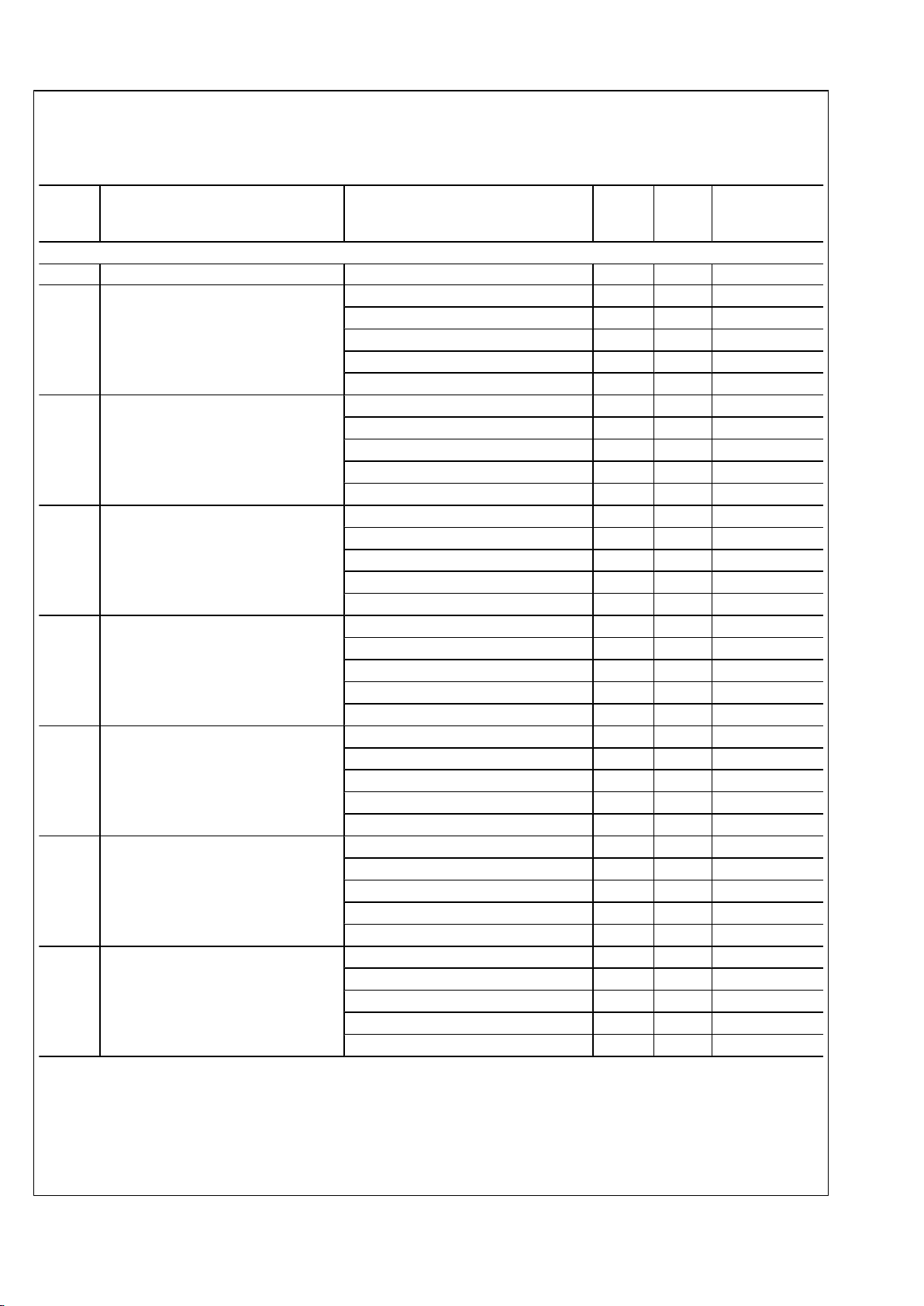
Dynamic Converter Electrical Characteristics
Unless otherwise specified, the following specifications apply: VIN = -1dBFS, AGND = DGND = DRGND = 0V, VA = VD = +3.3V,
VDR = +1.8V, Internal V
REF
= +1.0V, f
CLK
= 170 MHz, VCM = VRM, CL = 5 pF/pin, Single-Ended Clock Mode, Offset Binary Format.
Typical values are for TA = 25°C. Boldface limits apply for T
MIN
≤ TA ≤ T
MAX
. All other limits apply for TA = 25°C (Notes 7, 8, 9)
Symbol Parameter Conditions
Typical
(Note
10)
Limits
Units
(Limits)
DYNAMIC CONVERTER CHARACTERISTICS, AIN = -1dBFS
FPBW Full Power Bandwidth -1 dBFS Input, −3 dB Corner 1.1 GHz
SNR Signal-to-Noise Ratio
fIN = 10 MHz
67.5 dBFS
fIN = 70 MHz
67.2 66.0 dBFS
fIN = 150 MHz
67.1 dBFS
fIN = 250 MHz
66.8 dBFS
fIN = 400 MHz
66.0 dBFS
SFDR Spurious Free Dynamic Range
fIN = 10 MHz
86.6 dBFS
fIN = 70 MHz
85.4 74.0 dBFS
fIN = 150 MHz
83.4 dBFS
fIN = 250 MHz
84.1 dBFS
fIN = 400 MHz
72.9 dBFS
ENOB Effective Number of Bits
fIN = 10 MHz
10.9 Bits
fIN = 70 MHz
10.8 10.5 Bits
fIN = 150 MHz
10.8 Bits
fIN = 250 MHz
10.8 Bits
fIN = 400 MHz
10.5 Bits
THD Total Harmonic Disortion
fIN = 10 MHz
-82.6 dBFS
fIN = 70 MHz
−82.6 -72.0 dBFS
fIN = 150 MHz
-81.1 dBFS
fIN = 250 MHz
-80.3 dBFS
fIN = 400 MHz
-70.7 dBFS
H2 Second Harmonic Distortion
fIN = 10 MHz
-89.7 dBFS
fIN = 70 MHz
−88.4 -77.0 dBFS
fIN = 150 MHz
-93.5 dBFS
fIN = 250 MHz
-91.0 dBFS
fIN = 400 MHz
-72.9 dBFS
H3 Third Harmonic Distortion
fIN = 10 MHz
-86.7 dBFS
fIN = 70 MHz
−85.4 -74 dBFS
fIN = 150 MHz
-84.6 dBFS
fIN = 250 MHz
-84.1 dBFS
fIN = 400 MHz
-77.6 dBFS
SINAD Signal-to-Noise and Distortion Ratio
fIN = 10 MHz
67.3 dBFS
fIN = 70 MHz
67.1 65.2 dBFS
fIN = 150 MHz
67.0 dBFS
fIN = 250 MHz
66.6 dBFS
fIN = 400 MHz
64.7 dBFS
7 www.national.com
ADC12C170
 Loading...