

NSC ADC12662CIVF, ADC12662CIV Datasheet
ADC12662
12-Bit, 1.5 MHz, 200 mW A/D Converter
with Input Multiplexer and Sample/Hold
ADC12662 12-Bit, 1.5 MHz, 200 mW A/D Converter with Input Multiplexer and Sample/Hold
June 2001
General Description
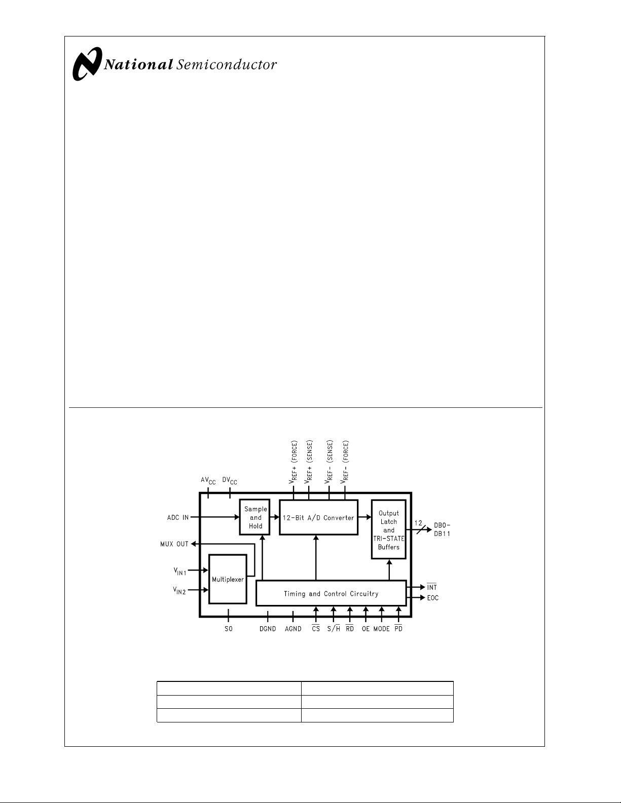
Using an innovative multistep conversion technique, the
12-bit ADC12662 CMOS analog-to-digital converter digitizes
signals at a 1.5 MHz sampling rate while consuming a maximum of only 200 mW on a single +5V supply. The
ADC12662 performs a 12-bit conversion in three
lower-resolution “flash” conversions, yielding a fast A/D without the cost and power dissipation associated with true flash
approaches.
The analog input voltage to the ADC12662 is tracked and
held by an internal sampling circuit, allowing high frequency
input signals to be accurately digitized without the need for
an external sample-and-hold circuit. The ADC12662 features
two sample-and-hold/flash comparator sections which allow
the converter to acquire one sample while converting the
previous. This pipelining technique increases conversion
speed without sacrificing performance. The multiplexer output is available to the user in order to perform additional
external signal processing before the signal is digitized.
When the converter is not digitizing signals, it can be placed
in the Standby mode; typical power consumption in this
mode is 250 µW.
ADC12662 Block Diagram
Features
n Built-in sample-and-hold
n Single +5V supply
n Single channel or 2 channel multiplexer operation
n Low Power Standby mode
Key Specifications
n Sampling rate 1.5 MHz (min)
n Conversion time 580 ns (typ)
n Signal-to-Noise Ratio, f
n Power consumption (f
n No missing codes over temperature Guaranteed
= 100 kHz 67.5 dB (min)
IN
= 1.5 MHz) 200 mW (max)
s
Applications
n Digital signal processor front ends
n Instrumentation
n Disk drives
n Mobile telecommunications
n Waveform digitizers
01187601
Ordering Information
Industrial (−40˚C ≤ TA≤ +85˚) Package
ADC12662CIV V44 Plastic Leaded Chip Carrier
ADC12662CIVF VGZ44A Plastic Quad Flat Package
© 2001 National Semiconductor Corporation DS011876 www.national.com
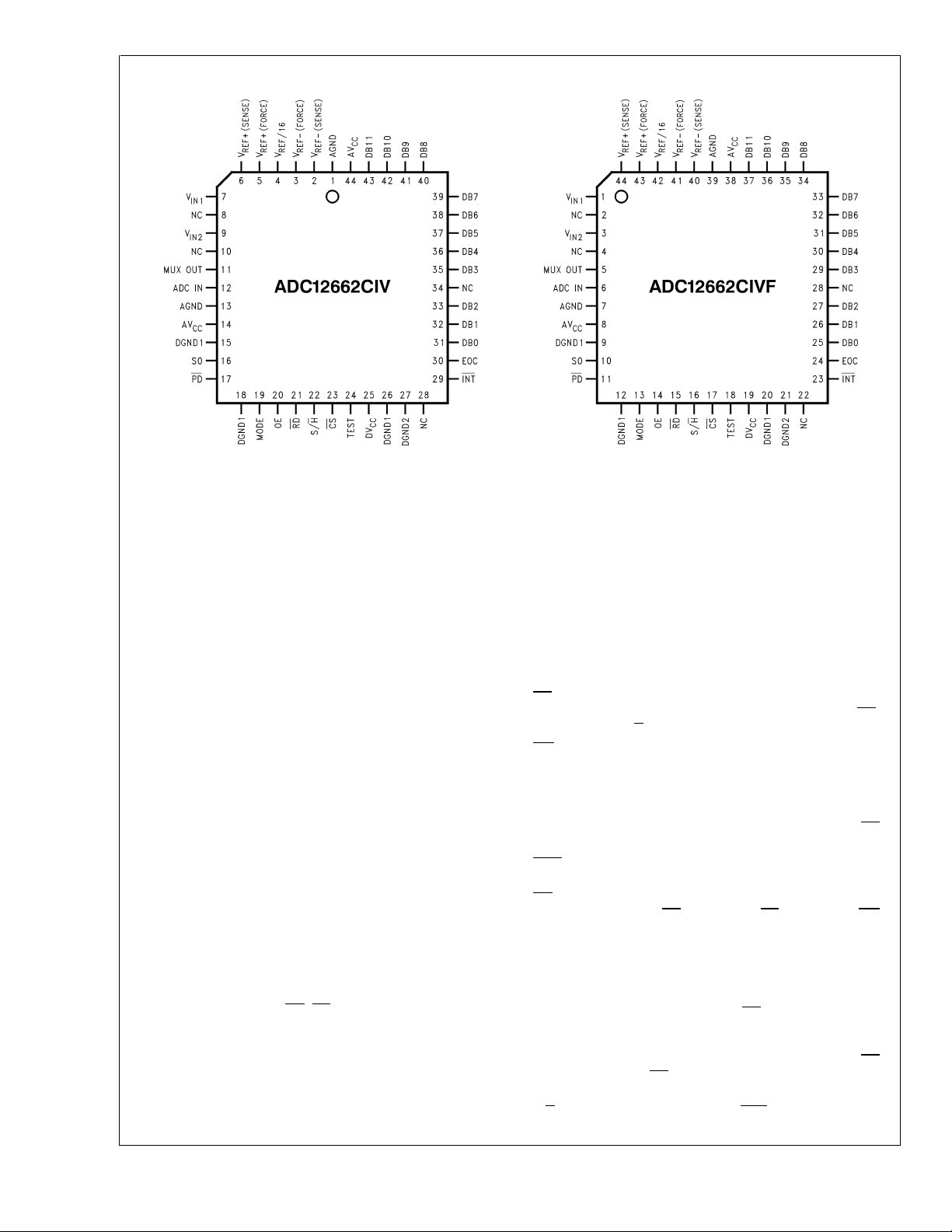
Connection Diagrams
ADC12662
Top View
01187615
Pin Descriptions
AV
CC
DV
CC
AGND, DGND1,
DB0–DB11 These are the TRI-STATE output pins, en-
V
IN1,VIN2
MUX OUT This is the output of the on-board analog
These are the two positive analog supply
inputs. They should always be connected to
the same voltage source, but are brought out
separately to allow for separate bypass capacitors. Each supply pin should be bypassed to AGND with a 0.1 µF ceramic capacitor in parallel with a 10 µF tantalum
capacitor.
This is the positive digital supply input. It
should always be connected to the same
voltage as the analog supply, AV
. It should
CC
be bypassed to DGND2 with a 0.1 µF ceramic capacitor in parallel with a 10 µF tantalum capacitor.
DGND2
These are the power supply ground pins.
There are separate analog and digital ground
pins for separate bypassing of the analog
and digital supplies. The ground pins should
be connected to a stable, noise-free system
ground. All of the ground pins should be
returned to the same potential. AGND is the
analog ground for the converter. DGND1 is
the ground pin for the digital control lines.
DGND2 is the ground return for the output
databus. See Section 6.0 LAYOUT AND
GROUNDING for more information.
abled by RD, CS, and OE.
These are the analog input pins to the multi-
plexer. For accurate conversions, no input
pin (even one that is not selected) should be
driven more than 50 mV below ground or 50
mV above V
.
CC
input multiplexer.
Top View
01187629
ADC IN This is the direct input to the 12-bit sampling
A/D converter. For accurate conversions,
this pin should not be driven more than 50
mV below ground or 50 mV above V
.
CC
S0 This pin selects the analog input that will be
connected to the ADC12662 during the conversion. The input is selected based on the
state of S0 when EOC makes its high-to-low
transition. Low selects V
V
.
IN2
, high selects
IN1
MODE This pin should be tied to DGND1.
CS
This is the active low Chip Select control
input. When low, this pin enables the RD,
S/H, and OE inputs. This pin can be tied low.
INT This is the active low Interrupt output. When
using the Interrupt Interface Mode (
Figure 1
this output goes low when a conversion has
been completed and indicates that the conversion result is available in the output
latches. This output is always high when RD
EOC
is held low (
This is the End-of-Conversion control output.
Figure 2
).
This output is low during a conversion.
RD
This is the active low Read control input.
When RD is low (and CS is low), the INT
output is reset and (if OE is high) data appears on the data bus. This pin can be tied
low.
OE This is the active high Output Enable control
input. This pin can be thought of as an inverted version of the RD input (see
Figure 6
Data output pins DB0–DB11 are TRI-STATE
when OE is low. Data appears on
DB0–DB11 only when OE is high and CS
and RD are both low. This pin can be tied
high.
S/H
This is the Sample/Hold control input. The
analog input signal is held and a new conver-
),
).
www.national.com 2

Pin Descriptions (Continued)
sion is initiated by the falling edge of this
control input (when CS is low).
PD This is the Power Down control input. This
pin should be held high for normal operation.
When this pin is pulled low, the device goes
into a low power standby mode.
V
REF+(FORCE)
,V
REF−(FORCE)
These are the positive and negative voltage
reference force inputs, respectively. See
Section 4, REFERENCE INPUTS, for more
information.
V
REF+(SENSE)
,V
REF−(SENSE)
These are the positive and negative voltage
reference sense pins, respectively. See Section 4, REFERENCE INPUTS, for more
information.
V
/16 This pin should be bypassed to AGND with a
REF
0.1 µF ceramic capacitor.
TEST This pin should be tied to DV
.
CC
ADC12662
www.national.com3
Absolute Maximum Ratings (Notes 1,
2)
If Military/Aerospace specified devices are required,
ADC12662
please contact the National Semiconductor Sales Office/
Distributors for availability and specifications.
Supply Voltage (V
) −0.3V to +6V
AV
CC
Voltage at Any Input or Output −0.3V to V
=DVCC=
CC
+
CC
VF Package
Vapor Phase (60 seconds) 215˚C
Infrared (15 seconds) 220˚C
Storage Temperature Range −65˚C to +150˚C
Maximum Junction Temperature
(T
) 150˚C
JMAX
Operating Ratings (Notes 1, 2)
0.3V
Input Current at Any Pin (Note 3) 25 mA
Package Input Current (Note 3) 50 mA
Power Dissipation (Note 4)
ADC12662CIV 875 mW
ESD Susceptibility (Note 5) 2000V
Temperature Range T
ADC12662CIV, ADC12662CIVF −40˚C ≤ TA≤
Supply Voltage Range
=AVCC) 4.75V to 5.25V
(DV
CC
MIN
Soldering Information (Note 6)
V Package, Infrared, 15 seconds +300˚C
Converter Characteristics
The following specifications apply for DVCC=AVCC= +5V, V
unless otherwise specified. Boldface limits apply for T
A=TJ
REF+(SENSE)
from T
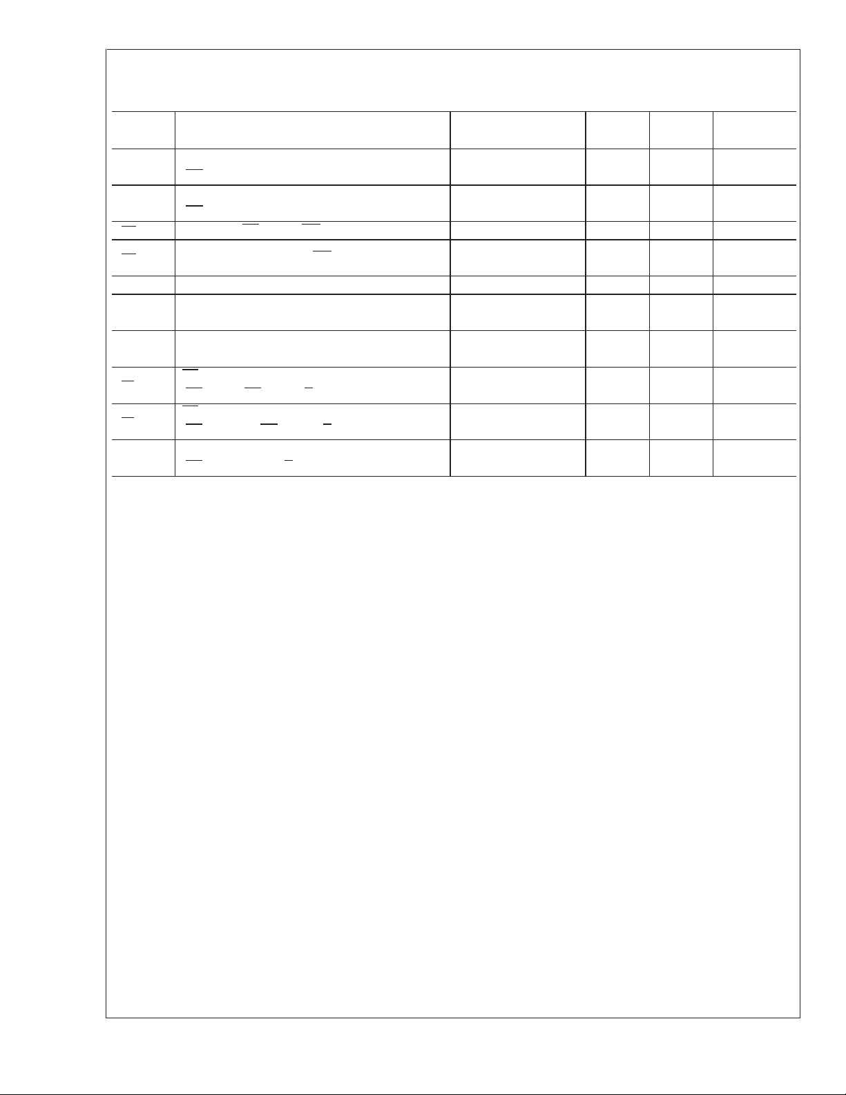
Symbol Parameter Conditions Typ Limit Units
Resolution 12 Bits
R
V
V
V
C
C
REF
REF(+)
REF(−)
IN
ADC
MUX
Differential Linearity Error T
Integral Linearity Error
(Note 9)
Offset Error T
Full-Scale Error T
Power Supply Sensitivity
(Note 15)
Reference Resistance 1000
V
REF+(SENSE)
V
REF−(SENSE)
Input Voltage AV
Input Voltage AGND V (min)
Input Voltage Range To V
ADC IN Input Leakage AGND to AV
ADC IN Input Capacitance 25 pF
MUX On-Channel Leakage AGND to AV
MUX Off-Channel Leakage AGND to AV
Multiplexer Input Cap 7 pF
MUX Off Isolation f
to T
T
DV
IN
MIN
MIN
MIN
MIN
MAX
to T
MAX
to T
MAX
to T
MAX
=AVCC=5V±5%
CC
IN1,VIN2
, or ADC IN
− 0.3V 0.1 3 µA (max)
CC
− 0.3V 0.1 3 µA (max)
CC
− 0.3V 0.1 3 µA (max)
CC
= 100 kHz 92 dB
= +4.096V, V
to T
MIN
REF−(SENSE)
; all other limits TA=TJ= +25˚C.
MAX
= AGND, and fs= 1.5 MHz,
(Note 7) (Note 8) (Limit)
±
0.4
±
0.4
±
0.3
±
0.3
±
0.95 LSB (max)
±
1.5 LSB (max)
±
2.0 LSB (max)
±
1.5 LSB (max)
±
0.75 LSB (max)
600 Ω (min)
1300 Ω (max)
CC
AV
+0.05V V (max)
CC
AGND − 0.05V V (min)
≤ TA≤ T
+85˚C
V (max)
MAX
Dynamic Characteristics (Note 10)
The following specifications apply for DVCC=AVCC= +5V, V
100 kHz, 0 dB from fullscale, and f
T
; all other limits TA=TJ= +25˚C.
MAX
= 1.5 MHz, unless otherwise specified. Boldface limits apply for TA=TJfrom T
s
REF+(SENSE)
Symbol Parameter Conditions Typ Limit Units
SINAD Signal-to-Noise Plus
Distortion Ratio
www.national.com 4
T
to T
MIN
MAX
= +4.096V, V
(Note 7) (Note 8) (Limit)
REF−(SENSE)
= AGND, RS=25Ω,fIN=
70 67.0 dB (min)
MIN
to
Dynamic Characteristics (Note 10) (Continued)
The following specifications apply for DVCC=AVCC= +5V, V
100 kHz, 0 dB from fullscale, and f
T
; all other limits TA=TJ= +25˚C.
MAX
= 1.5 MHz, unless otherwise specified. Boldface limits apply for TA=TJfrom T
s
REF+(SENSE)
Symbol Parameter Conditions Typ Limit Units
SNR Signal-to-Noise Ratio
(Note 11)
THD Total Harmonic Distortion
(Note 12)
ENOB Effective Number of Bits
(Note 13)
IMD Intermodulation Distortion f
T
to T
MIN
T
MIN
T
MIN
IN
MAX
to T
MAX
to t
MAX
= 88.7 kHz, 89.5 kHz −80 dBc
= +4.096V, V
(Note 7) (Note 8) (Limit)
REF−(SENSE)
= AGND, RS=25Ω,fIN=
70 67.5 dB (min)
−80 −70 dBc (max)
11.3 10.8 Bits (min)
DC Electrical Characteristics
The following specifications apply for DVCC=AVCC= +5V, V
unless otherwise specified. Boldface limits apply for T
A=TJ
REF+(SENSE)
from T
Symbol Parameter Conditions Typ Limit Units
V
IN(1)
V
IN(0)
I
IN(1)
I
IN(0)
V
OUT(1)
V
OUT(0)
I
OUT
C
OUT
C
IN
DI
CC
AI
CC
I
STANDBY
Logical “1” Input Voltage DVCC=AVCC= +5.5V 2.0 V (min)
Logical “0” Input Voltage DVCC=AVCC= +4.5V 0.8 V (max)
Logical “1” Input Current 0.1 1.0 µA (max)
Logical “0” Input Current 0.1 1.0 µA (max)
=AVCC= +4.5V,
DV
CC
Logical “1” Output Voltage
Logical “0” Output Voltage
TRI-STATE®Output
Leakage Current
I
= −360 µA 2.4 V (min)
OUT
I
= −100 µA 4.25 V (min)
OUT
DV
=AVCC= +4.5V,
CC
= 1.6 mA
I
OUT
Pins DB0–DB11 0.1 3 µA (max)
TRI-STATE Output Capacitance Pins DB0–DB11 5 pF
Digital Input Capacitance 4 pF
DVCCSupply Current 2 3 mA (max)
AVCCSupply Current 32 37 mA (max)
Standby Current (DICC+AICC) PD=0V 50 µA
= +4.096V, V
to T
MIN
REF−(SENSE)
; all other limits TA=TJ= +25˚C.
MAX
= AGND, and fs= 1.5 MHz,
(Note 7) (Note 8) (Limit)
0.4 V (max)
MIN
ADC12662
to
AC Electrical Characteristics
The following specifications apply for DVCC=AVCC= +5V, V
unless otherwise specified. Boldface limits apply for T
A=TJ
REF+(SENSE)
from T
Symbol Parameter Conditions Typ Limit Units
f
s
t
CONV
t
AD
t
S/H
t
EOC
Maximum Sampling Rate
(1/t
THROUGHPUT
)
Conversion Time
(S/H Low to EOC High)
Aperture Delay
(S/H Low to Input Voltage Held)
S/H Pulse Width 10
S/H Low to EOC Low 90
= +4.096V, V
to T
MIN
REF−(SENSE)
; all other limits TA=TJ= +25˚C.
MAX
= AGND, and fs= 1.5 MHz,
(Note 7) (Note 8) (Limits)
1.5 MHz (min)
580
510 ns (min)
660 ns (max)
20 ns
400 ns (max)
60 ns (min)
126 ns (max)
5 ns (min)
www.national.com5
AC Electrical Characteristics (Continued)
The following specifications apply for DVCC=AVCC= +5V, V
unless otherwise specified. Boldface limits apply for T
ADC12662
Symbol Parameter Conditions Typ Limit Units
t
ACC
t1H,t
t
INTH
t
INTL
t
UPDATE
t
MS
t
MH
t
CSS
t
CSH
t
WU
Note 1: Absolute Maximum Ratings indicate limits beyond which damage to the device may occur. Operating Ratings indicate conditions for which the device is
functional. These ratings do not guarantee specific performance limits, however.For guaranteed specifications and test conditions, see the Electrical Characteristics.
The guaranteed specifications apply only for the test conditions listed. Some performance characteristics may degrade when the device is not operated under the
listed test conditions.
Note 2: All voltages are measured with respect to GND (GND = AGND = DGND), unless otherwise specified.
Note 3: When the input voltage (V
to 25 mA or less. The 50 mA package input current limits the number of pins that can safely exceed the power supplies with an input current of 25 mA to two.
Note 4: The maximum power dissipation must be derated at elevated temperatures and is dictated by T
allowable power dissipation at any temperature is P
(PLCC) package is 55˚C/W. θ
conditions.
Note 5: Human body model, 100 pF discharged through a 1.5 kΩ resistor. Machine model ESD rating is 200V.
Note 6: See AN-450 “Surface Mounting Methods and Their Effect on Product Reliability” or the section titled “Surface Mount” found in a current National
Semiconductor Linear Data Book for other methods of soldering surface mount devices.
Note 7: Typicals are at +25˚C and represent most likely parametric norm.
Note 8: Tested limits are guaranteed to National’s AOQL (Average Outgoing Quality Level).
Note 9: Integral Linearity Error is the maximum deviation from a straight line between the
Note 10: Dynamic testing of the ADC12662 is done using the ADC IN input. The input multiplexer adds harmonic distortion at high frequencies. See the graph in
the Typical Performance Characteristics section for a typical graph of THD performance vs input frequency with and without the input multiplexer.
Note 11: The signal-to-noise ratio is the ratio of the signal amplitude to the background noise level. Harmonics of the input signal are not included in its calculation.
Note 12: The contributions from the first nine harmonics are used in the calculation of the THD.
Note 13: Effective Number of Bits (ENOB) is calculated from the measured signal-to-noise plus distortion ratio (SINAD) using the equation ENOB = (SINAD −
1.76)/6.02.
Note 14: The digital power supply current takes up to 10 seconds to decay to its final value after PD is pulled low. This prohibits production testing of the standby
current. Some parts may exhibit significantly higher standby currents than the 50 µA typical.
Note 15: Power Supply Sensitivity is defined as the change in the Offset Error or the Full Scale Error due to a change in the supply voltage.
Access Time
(RD Low or OE High to Data Valid)
TRI-STATE Control
0H
(RD High or OE Low to Databus TRI-STATE)
Delay from RD Low to INT High CL= 100 pF 35 60 ns (max)
Delay from EOC High to INT Low CL= 100 pF −25
EOC High to New Data Valid 5 15 ns (max)
Multiplexer Address Setup Time
(MUX Address Valid to EOC Low)
Multiplexer Address Hold Time
(EOC Low to MUX Address Invalid)
CS Setup Time
(CS Low to RD Low, S/H Low, or OE High)
CS Hold Time
(CS High after RD High, S/H High, or OE Low)
Wake-Up Time
(PD High to First S/H Low)
) at any pin exceeds the power supply rails (V
IN
=(T
for the VF (PQFP) package is 62˚C/W. In most cases the maximum derated power dissipation will be reached only during fault
JA
D
)/θJAor the number given in the Absolute Maximum Ratings, whichever is lower. θJAfor the V
JMAX−TA
A=TJ
REF+(SENSE)
from T
C
L
R
L
<
IN
= +4.096V, V
to T
MIN
REF−(SENSE)
; all other limits TA=TJ= +25˚C.
MAX
= AGND, and fs= 1.5 MHz,
(Note 7) (Note 8) (Limits)
= 100 pF 10 20 ns (max)
= 1k, CL=10pF 25 40 ns (max)
−35 ns (min)
−5 ns (max)
50 ns (min)
50 ns (min)
20 ns (min)
20 ns (min)
1µs
GND or V
>
VCC) the absolute value of current at that pin should be limited
IN
, θJAand the ambient temperature TA. The maximum
JMAX
measured
offset and full scale endpoints.
www.national.com 6
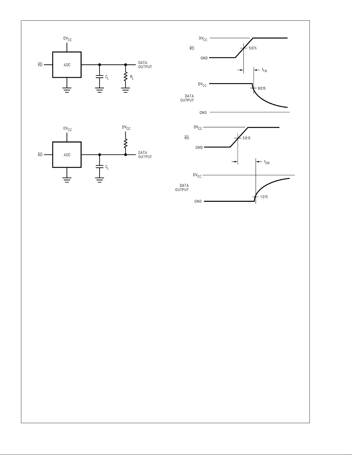
TRI-STATE Test Circuit and Waveforms
01187602
ADC12662
01187603
01187604
01187605
www.national.com7
 Loading...