NSC ADC12181CIVT Datasheet

March 2000
ADC12181
12-Bit, 10 MHz Self-Calibrating, Pipelined A/D Converter
with Internal Sample & Hold
ADC12181 12-Bit, 10 MHz Self-Calibrating, Pipelined A/D Converter with Internal Sample & Hold
General Description
The ADC12181 is a monolithic CMOS analog-to-digital converter capable of converting analog input signals into 12-bit
digital words at 10 megasamples per second (MSPS). The
ADC12181 utilizes an innovative pipeline architecture to
minimize die size and power consumption. Self-calibration
and error correction maintain accuracy and performance
over temperature.
The ADC12181 converter operates on a 5V power supply
and can digitize analog input signals in the range of 0 to 2V.
A single convert clock controls the conversion operation. All
digital I/O is TTL compatible.
The ADC12181 is designed to minimize external components necessary for the analog input interface. An internal
sample-and-hold circuit samples the analog input and an internal amplifier buffers the reference voltage input.
The ADC12181 is available in the 32-lead TQFP package
and is designed to operate over the extended commercial
temperature range of -40˚C to +85˚C.
Features
n Single 5V power supply
n Simple analog input interface
n Internal Sample-and-hold
n Internal Reference buffer amplifier
n Low power consumption
Key Specifications
n Resolution 12 Bits
n Conversion Rate 10 Msps (min)
n DNL
n SNR 65 dB (typ)
n ENOB 10.4 Bits (typ)
n Analog Input Range 2 Vpp (min)
n Supply Voltage +5V
n Power Consumption, 10 MHz 235 mW (typ)
±
0.4 LSB (typ)
±
Applications
n Image processing front end
n PC-based data acquisition
n Scanners
n Fax machines
n Waveform digitizer
5%
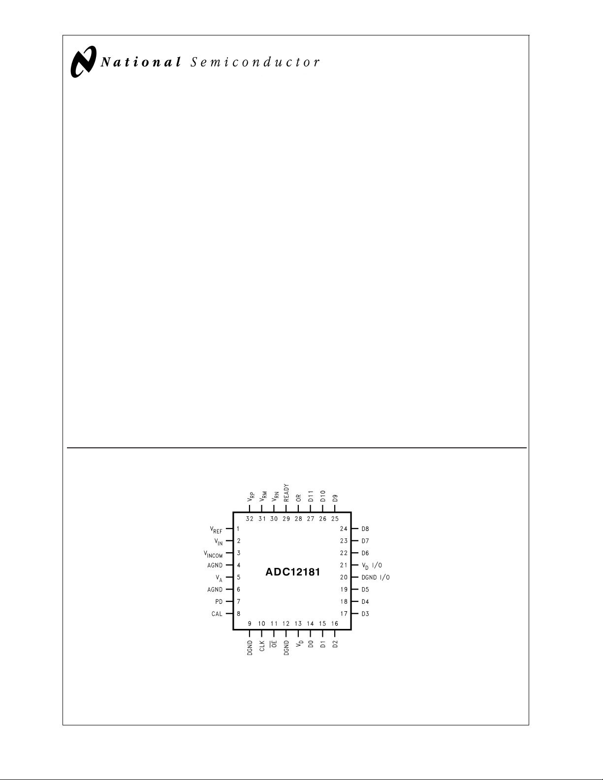
Connection Diagram
DS101039-1
TRI-STATE®is a registered trademark of National Semiconductor Corporation.
© 2000 National Semiconductor Corporation DS101039 www.national.com

Ordering Information
Industrial
ADC12181
ADC12181CIVT 32 pin TQFP
ADC12181 EVAL Evaluation Board
(−40˚C ≤ TA ≤ +85˚C)
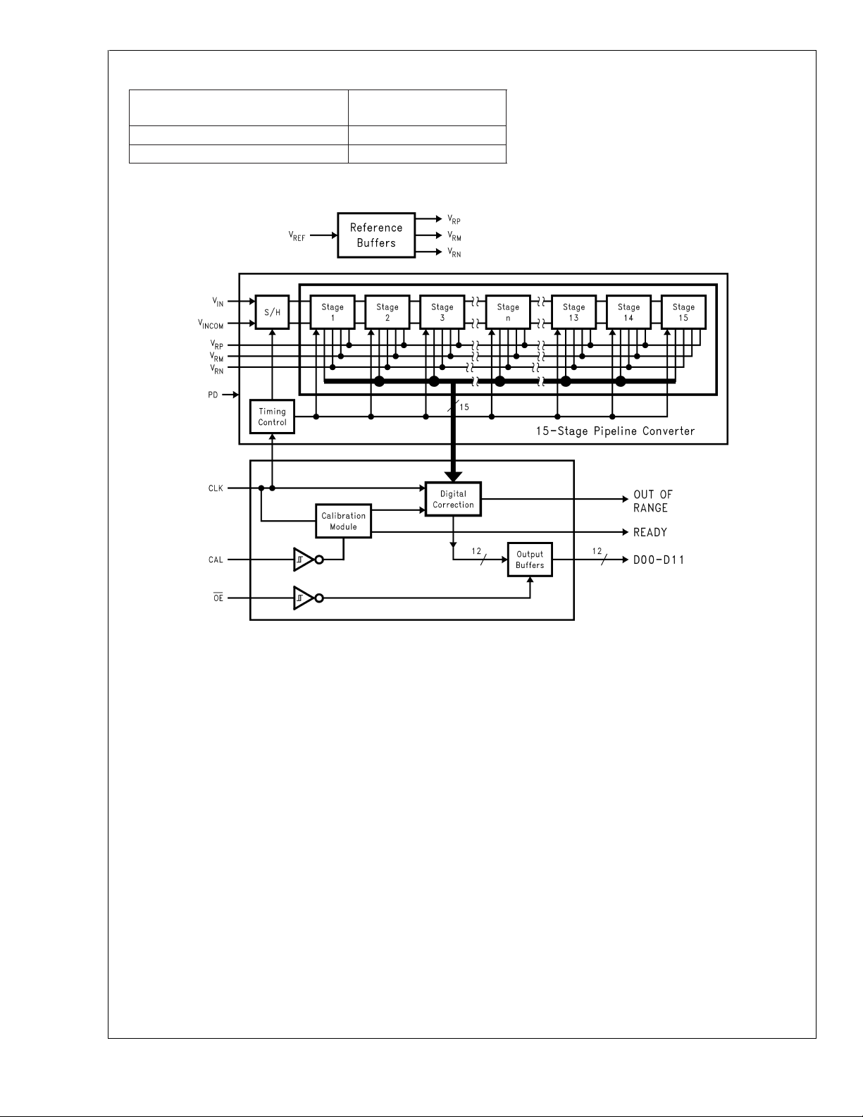
Simplified Block Diagram
Package
DS101039-2
www.national.com 2

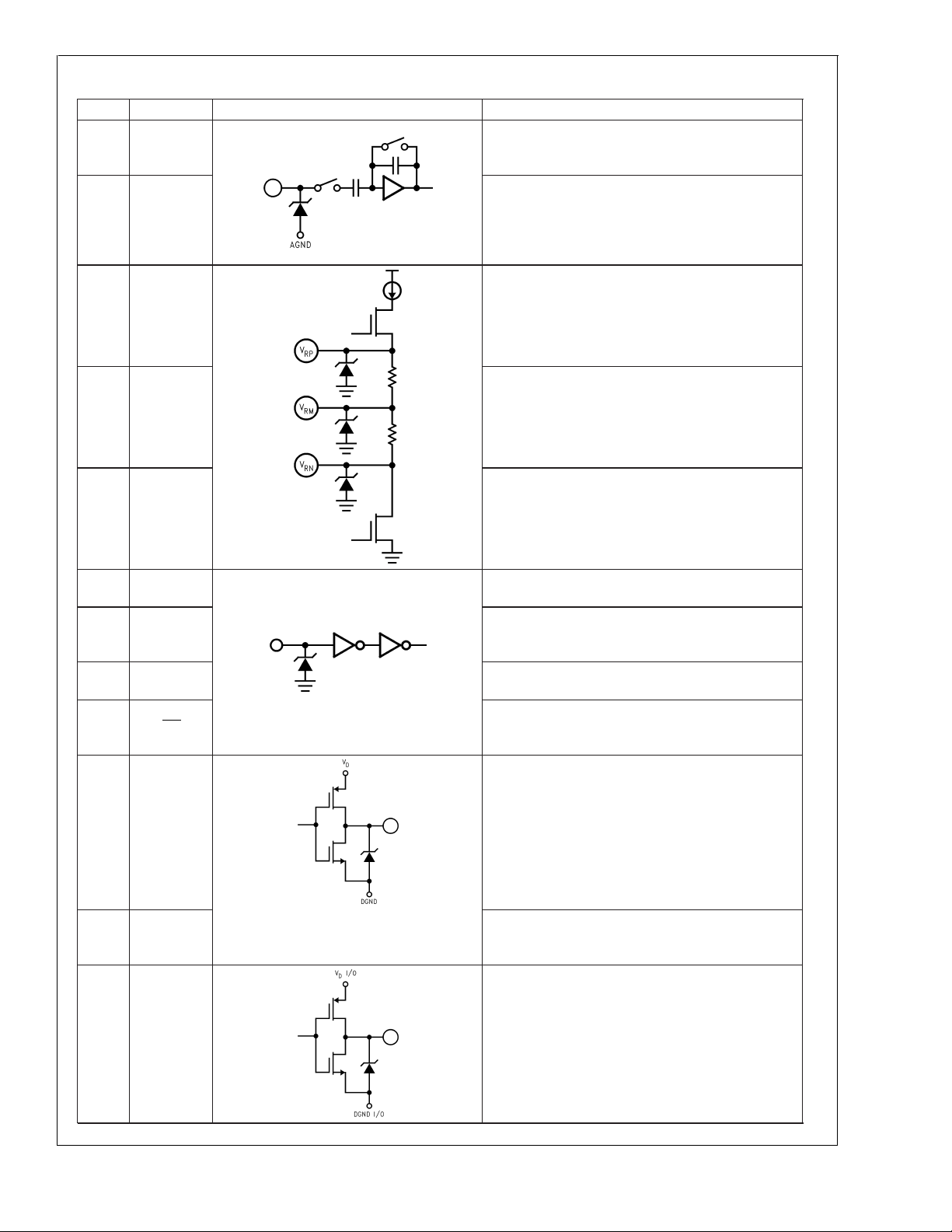
Pin Descriptions and Equivalent Circuits #2
No. Symbol Equivalent Circuit Description
Analog signal input. With a 2.0V reference voltage,
2V
1V
32 V
31 V
IN
REF
RP
RM
input signal voltages in the range of 0 to 2.0 Volts
will be converted. See section 1.2.
Reference voltage input. This pin should be driven
from an accurate, stable reference source in the
range of 1.8 to 2.2V and bypassed to a low-noise
analog ground with a monolithic ceramic capacitor,
nominally 0.01µF. See section 1.1.
Positive reference bypass pin. Bypass with a 0.1µF
capacitor. Do not connect anything else to this pin.
See section 3.1
Reference midpoint bypass pin. Bypass with a
0.1µF capacitor. Do not connect anything else to
this pin. See section 3.1
ADC12181
30 V
RN
10 CLOCK
8 CAL
7PD
11 OE
28 OR
29 READY
Negative reverence bypass pin. Bypass with a
0.1µF capacitor. Do not connect anything else to
this pin. See section 3.1
Sample Clock input, TTL compatible. Maximum
amplitude should not exceed 3V.
Calibration request, active High. Calibration cycle
starts when CAL returns to logic low. CAL is ignored
during power-down mode. See section 2.2.
Power-down, active High, ignored during calibration
cycle. See paragraph 2.4
Output enable control, active low. When this pin is
high the data outputs are in Tri-state
(high-impedance) mode.
Over range indicator. This pin is at a logic High for
V
IN
<
0 or for V
>
V
REF
.
IN
Device ready indicator, active High. This pin is at a
logic Low during a calibration cycle and while the
device is in the power down mode.
14-19,
22-27
D0 - D11
Digital output word, CMOS compatible. D0 (pin 14)
is LSB, D11 (pin 27) is MSB. Load with no more
than 50pF.
www.national.com3

Pin Descriptions and Equivalent Circuits #2 (Continued)
ADC12181
No. Symbol Equivalent Circuit Description
3V
5V
4, 6 AGND
13 V
9, 12 DGND
21 V
20 DGND I/O
IN com
A
D
I/O
D
Analog input common. Connect to a quiet point in
analog ground near the driving device. See section
1.2.
Positive analog supply pin. Connect to a clean,
quiet voltage source of +5V. V
and VDshould have
A
a common supply and be separately bypassed with
a 5µF to 10µF capacitor and a 0.1µF chip capacitor.
The ground return for the analog supply. AGND and
DGND should be connected together close to the
ADC12181 package. See section 5.0.
Positive analog supply pin. Connect to a clean,
quiet voltage source of +5V. V
and VDshould have
A
a common supply and be separately bypassed with
a 5µF to 10µF capacitor and a 0.1 µF chip
capacitor.
The ground return for the analog supply. AGND and
DGND should be connected together close to the
ADC12181 package. See section 5.0
The digital output driver supply pin. This pin can be
operated from a supply voltage of 3V to 5V, but the
voltage on this pin should never exceed the V
D
supply pin voltage.
The ground return for the output drivers. This pin
should be returned to a point in the digital ground
that is removed from the other ground pins of the
ADC12181.
www.national.com 4

ADC12181
Absolute Maximum Ratings (Notes 1, 2)
If Military/Aerospace specified devices are required,
Storage Temp. −65˚C to +150˚C
Maximum Junction Temp. 150˚C
please contact the National Semiconductor Sales Office/
Distributors for availability and specifications.
Supply Voltage 6.5V
Voltage on Any Output −0.3V to V
Input Current at Any Pin (Note 3)
Package Input Current (Note 3)
+
+0.3V
±
25mA
±
50mA
Package Dissipation See (Note 4)
ESD Susceptibility
Operating Ratings
Operating Temp. Range −40˚C ≤ TA≤ +85˚C
Supply Voltage +4.75V to +5.25V
V
I/O +2.7V to V
D
V
Input 1.8V to 2.2V
REF
CLOCK, CAL, PD, OE −0.05V to V
|AGND −DGND| ≤100mV
+ 0.05V
D
Human Body Model 1500V
Machine Model 200V
Soldering Temp., Infrared, 10
300˚C
sec.(Note 6)
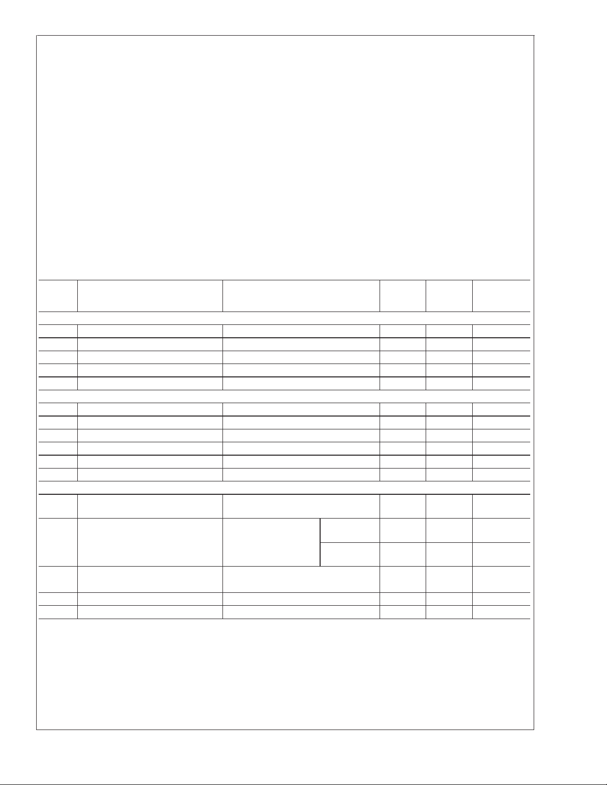
Converter Electrical Characteristics
The following specifications apply for AGND = DGND = DGND I/O = 0V, VA=VD=VDI/O = +5V, PD = +5V, V
f
= 10MHz, CL= 50 pF/pin. After Auto-Cal at Temperature. Boldface limits apply for TA=TJto T
CLK
limits TA=TJ= 25˚C (Notes 7, 8) and (Note 9)
Symbol Parameter Conditions
Typical
(Note
10)
MIN
Limits
(Note
11)
to T
Static Converter Characteristics
Resolution with No Missing Codes 12 Bits(min)
INL Integral Non Linearity
DNL Differential Non Linearity
Full-Scale Error
Zero Error
±
±
±
±
0.7
0.4
0.05
0.15
±
2.1 LSB( max)
±
0.8 LSB( max)
±
0.24 %FS(max)
±
0.24 %FS(max)
Dynamic Converter Characteristics
BW Full Power Bandwidth 100 MHz
SNR Signal-to-Noise Ratio f
SINAD Signal-to-Noise & Distortion f
ENOB Effective Number of Bits f
THD Total Hamonic Distortion f
SFDR Spurious Free Dynamic Range f
= 5 MHz, VIN= 2.0V
in
= 5 MHz, VIN= 2.0V
in
= 5 MHz, VIN= 2.0V
in
= 5 MHz, VIN= 2.0V
in
= 5 MHz, VIN= 2.0V
in
P-P
P-P
P-P
P-P
P-P
65 62 dB
64.5 61.5 dB
10.4 10 Bits
74 dB
73 dB
Reference and Analog Input Characteristics
V
IN
C
IN
V
REF
Input Voltage Range V
VINInput Capacitance
= 2.0V
REF
V
= 1.0Vdc +
IN
0.7Vrms
(CLK
LOW)
(CLK
HIGH)
10 pF
15 pF
Reference Voltage (Note 14) 2.00
0
V
REF
1.8 V(min)
2.2 V(max)
Reference Input Leakage Current 10 µA
Reference Input Resistance 1 MΩ(min)
REF
MAX
= +2.0V,
: all other
Units
(Limits)
V(min)
V(max)
D
www.national.com5
 Loading...