

ADC0801/ADC0802/ADC0803/ADC0804/ADC0805
8-Bit µP Compatible A/D Converters
General Description
The ADC0801, ADC0802, ADC0803, ADC0804 and
ADC0805 are CMOS 8-bit successive approximation A/D
converters that use a differential potentiometric
ladder—similar to the 256R products. These converters are
designed to allow operation with the NSC800 and INS8080A
derivative control bus with TRI-STATE
®
output latches directly driving the data bus. These A/Ds appear like memory
locations or I/O ports to the microprocessor and no interfacing logic is needed.
Differential analog voltage inputs allow increasing the
common-mode rejection and offsetting the analog zero input
voltage value. In addition, the voltage reference input can be
adjusted to allow encoding any smaller analog voltage span
to the full 8 bits of resolution.
Features
n Compatible with 8080 µP derivatives— no interfacing
logic needed - access time - 135 ns
n Easy interface to all microprocessors, or operates “stand
alone”
n Differential analog voltage inputs
n Logic inputs and outputs meet both MOS and TTL
voltage level specifications
n Works with 2.5V (LM336) voltage reference
n On-chip clock generator
n 0V to 5V analog input voltage range with single 5V
supply
n No zero adjust required
n 0.3" standard width 20-pin DIP package
n 20-pin molded chip carrier or small outline package
n Operates ratiometrically or with 5 V
DC
, 2.5 VDC,or
analog span adjusted voltage reference
Key Specifications
n Resolution 8 bits
n Total error
±
1
⁄4LSB,
±
1
⁄2LSB and±1 LSB
n Conversion time 100 µs
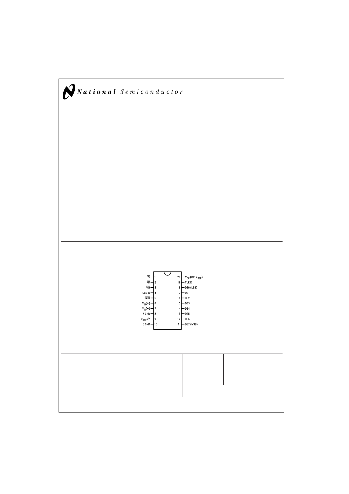
Connection Diagram
Ordering Information
TEMP RANGE 0˚C TO 70˚C 0˚C TO 70˚C −40˚C TO +85˚C
±
1
⁄4Bit Adjusted ADC0801LCN
ERROR
±
1
⁄2Bit Unadjusted ADC0802LCWM ADC0802LCN
±
1
⁄2Bit Adjusted ADC0803LCN
±
1Bit Unadjusted ADC0804LCWM ADC0804LCN ADC0805LCN/ADC0804LCJ
PACKAGE OUTLINE M20B—Small
Outline
N20A—Molded DIP
TRI-STATE®is a registered trademark of National Semiconductor Corp.
Z-80
®
is a registered trademark of Zilog Corp.
ADC080X
Dual-In-Line and Small Outline (SO) Packages
DS005671-30
See Ordering Information
November 1999
ADC0801/ADC0802/ADC0803/ADC0804/ADC0805 8-Bit µP Compatible A/D Converters
© 1999 National Semiconductor Corporation DS005671 www.national.com
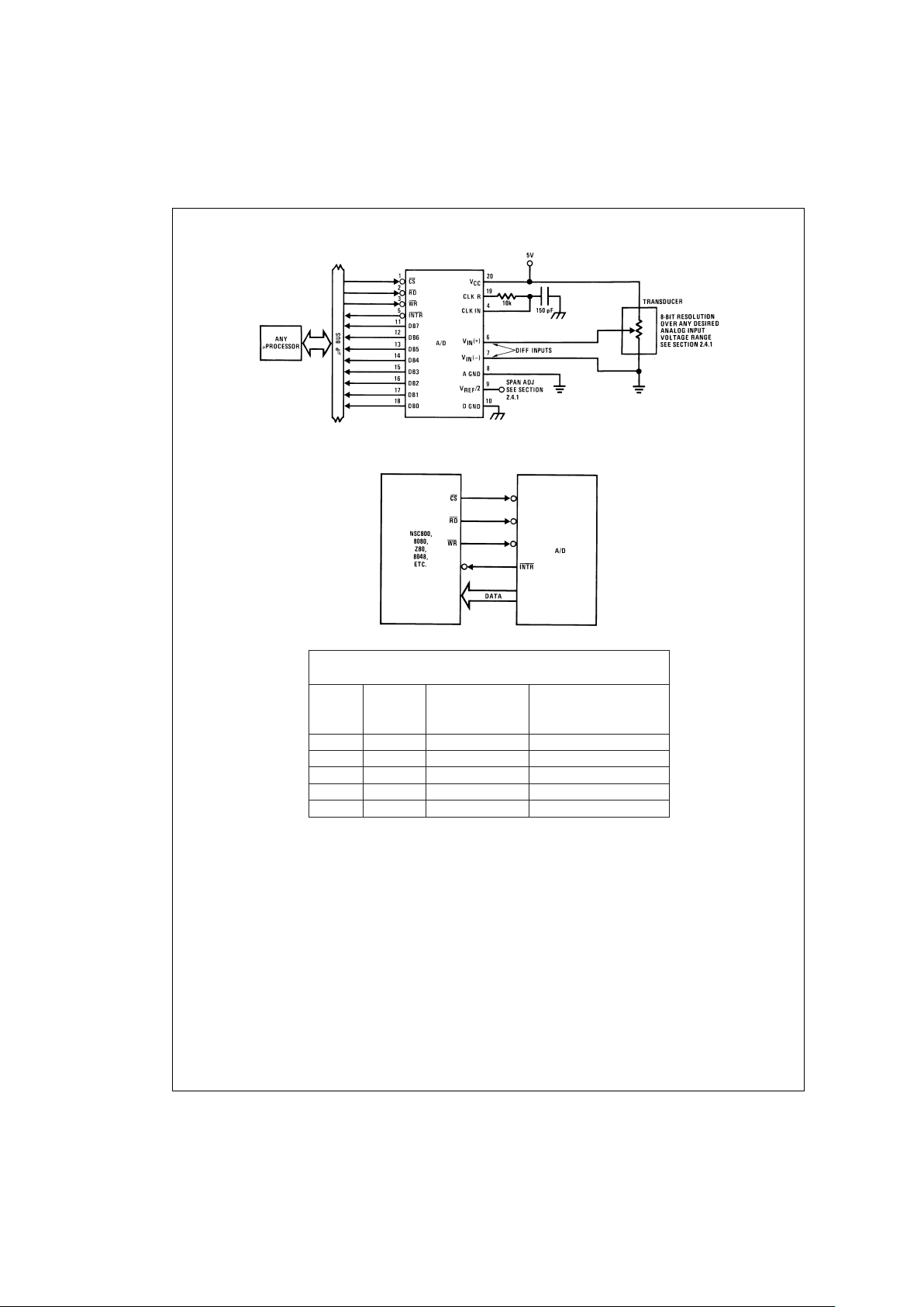
Typical Applications
Error Specification (Includes Full-Scale,
Zero Error, and Non-Linearity)
Part Full- V
REF
/2=2.500 V
DCVREF
/2=No Connection
Number Scale (No Adjustments) (No Adjustments)
Adjusted
ADC0801
±
1
⁄4LSB
ADC0802
±
1
⁄2LSB
ADC0803
±
1
⁄2LSB
ADC0804
±
1 LSB
ADC0805
±
1 LSB
DS005671-1
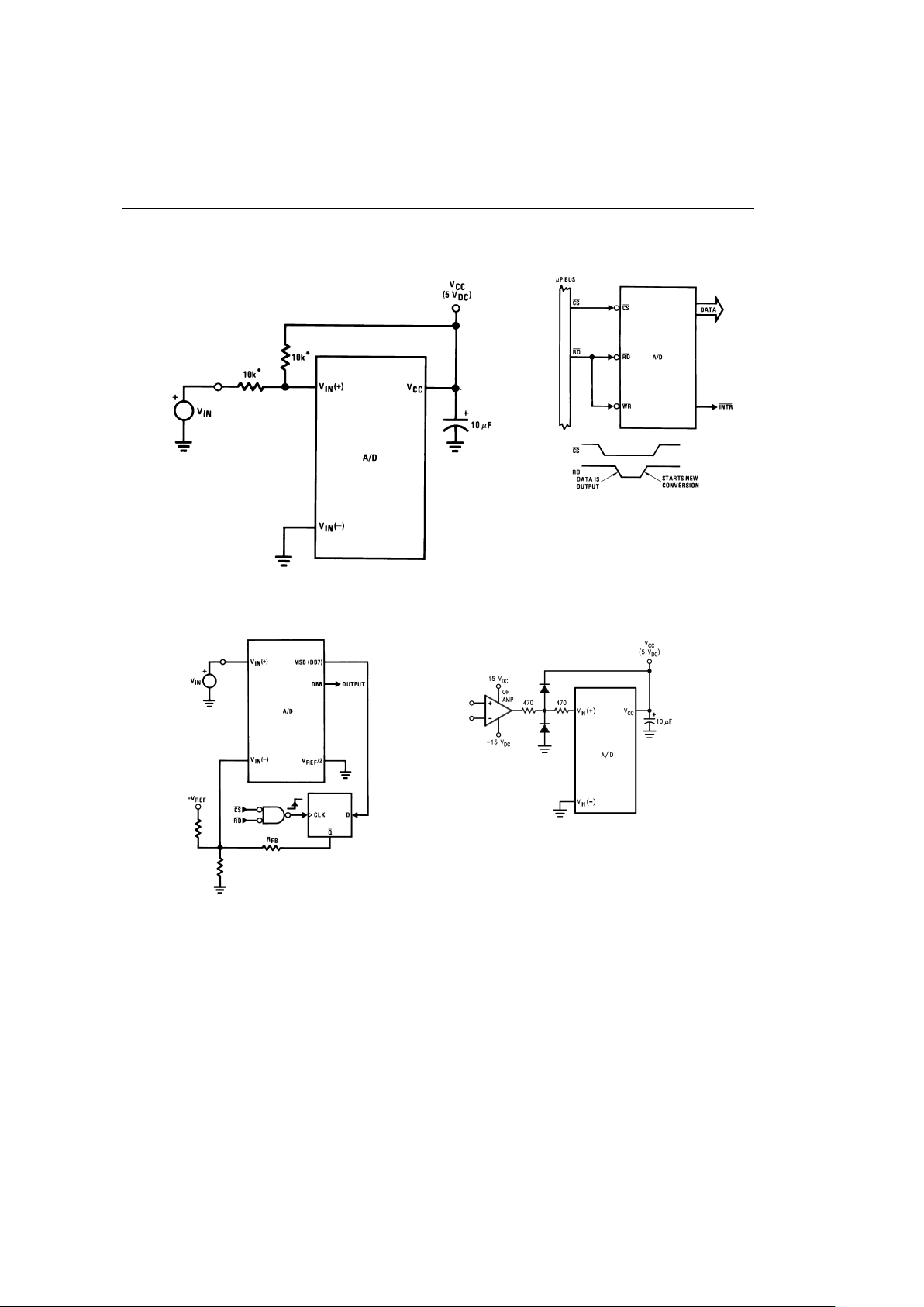
8080 Interface
DS005671-31
ADC0801/ADC0802/ADC0803/ADC0804/ADC0805
www.national.com 2
Absolute Maximum Ratings (Notes 1, 2)
If Military/Aerospace specified devices are required,
please contact the National Semiconductor Sales Office/
Distributors for availability and specifications.
Supply Voltage (V
CC
) (Note 3) 6.5V
Voltage
Logic Control Inputs −0.3V to +18V
At Other Input and Outputs −0.3V to (V
CC
+0.3V)
Lead Temp. (Soldering, 10 seconds)
Dual-In-Line Package (plastic) 260˚C
Dual-In-Line Package (ceramic) 300˚C
Surface Mount Package
Vapor Phase (60 seconds) 215˚C
Infrared (15 seconds) 220˚C
Storage Temperature Range −65˚C to +150˚C
Package Dissipation at T
A
=
25˚C 875 mW
ESD Susceptibility (Note 10) 800V
Operating Ratings (Notes 1, 2)
Temperature Range T
MIN≤TA≤TMAX
ADC0804LCJ −40˚C≤TA≤+85˚C
ADC0801/02/03/05LCN −40˚C≤T
A
≤+85˚C
ADC0804LCN 0˚C≤T
A
≤+70˚C
ADC0802/04LCWM 0˚C≤T
A
≤+70˚C
Range of V
CC
4.5 VDCto 6.3 V
DC
Electrical Characteristics
The following specifications apply for V
CC
=
5V
DC,TMIN≤TA≤TMAX
and f
CLK
=
640 kHz unless otherwise specified.
Parameter Conditions Min Typ Max Units
ADC0801: Total Adjusted Error (Note 8) With Full-Scale Adj.
±
1
⁄
4
LSB
(See Section 2.5.2)
ADC0802: Total Unadjusted Error (Note 8) V
REF
/2=2.500 V
DC
±
1
⁄
2
LSB
ADC0803: Total Adjusted Error (Note 8) With Full-Scale Adj.
±
1
⁄
2
LSB
(See Section 2.5.2)
ADC0804: Total Unadjusted Error (Note 8) V
REF
/2=2.500 V
DC
±
1 LSB
ADC0805: Total Unadjusted Error (Note 8) V
REF
/2-No Connection
±
1 LSB
V
REF
/2 Input Resistance (Pin 9) ADC0801/02/03/05 2.5 8.0 kΩ
ADC0804 (Note 9) 0.75 1.1 kΩ
Analog Input Voltage Range (Note 4) V(+) or V(−) Gnd–0.05 V
CC
+0.05 V
DC
DC Common-Mode Error Over Analog Input Voltage
±
1/16
±
1
⁄
8
LSB
Range
Power Supply Sensitivity V
CC
=
5V
DC
±
10%Over
±
1/16
±
1
⁄
8
LSB
Allowed V
IN
(+) and VIN(−)
Voltage Range (Note 4)
AC Electrical Characteristics
The following specifications apply for V
CC
=
5V
DC
and T
MIN≤TA≤TMAX
unless otherwise specified.
Symbol Parameter Conditions Min Typ Max Units
T
C
Conversion Time f
CLK
=
640 kHz (Note 6) 103 114 µs
T
C
Conversion Time (Notes 5, 6) 66 73 1/f
CLK
f
CLK
Clock Frequency V
CC
=
5V, (Note 5) 100 640 1460 kHz
Clock Duty Cycle 40 60
%
CR Conversion Rate in Free-Running INTR tied to WR with
8770 9708 conv/s
Mode CS=0V
DC,fCLK
=
640 kHz
t
W(WR)L
Width of WR Input (Start Pulse Width) CS=0VDC(Note 7) 100 ns
t
ACC
Access Time (Delay from Falling C
L
=
100 pF 135 200 ns
Edge of RD to Output Data Valid)
t1H,t
0H
TRI-STATE Control (Delay C
L
=
10 pF, R
L
=
10k 125 200 ns
from Rising Edge of RD to
(See TRI-STATE Test
Hi-Z State) Circuits)
t
WI,tRI
Delay from Falling Edge 300 450 ns
of WR or RD to Reset of INTR
C
IN
Input Capacitance of Logic 5 7.5 pF
Control Inputs
ADC0801/ADC0802/ADC0803/ADC0804/ADC0805
www.national.com3
AC Electrical Characteristics (Continued)
The following specifications apply for V
CC
=
5V
DC
and T
MIN≤TA≤TMAX
unless otherwise specified.
Symbol Parameter Conditions Min Typ Max Units
C
OUT
TRI-STATE Output 5 7.5 pF
Capacitance (Data Buffers)
CONTROL INPUTS [Note: CLK IN (Pin 4) is the input of a Schmitt trigger circuit and is therefore specified separately]
V
IN
(1) Logical “1” Input Voltage V
CC
=
5.25 V
DC
2.0 15 V
DC
(Except Pin 4 CLK IN)
V
IN
(0) Logical “0” Input Voltage V
CC
=
4.75 V
DC
0.8 V
DC
(Except Pin 4 CLK IN)
I
IN
(1) Logical “1” Input Current V
IN
=
5V
DC
0.005 1 µA
DC
(All Inputs)
I
IN
(0) Logical “0” Input Current V
IN
=
0V
DC
−1 −0.005 µA
DC
(All Inputs)
CLOCK IN AND CLOCK R
V
T
+ CLK IN (Pin 4) Positive Going 2.7 3.1 3.5 V
DC
Threshold Voltage
V
T
− CLK IN (Pin 4) Negative 1.5 1.8 2.1 V
DC
Going Threshold Voltage
V
H
CLK IN (Pin 4) Hysteresis 0.6 1.3 2.0 V
DC
(VT+)−(VT−)
V
OUT
(0) Logical “0” CLK R Output I
O
=
360 µA 0.4 V
DC
Voltage V
CC
=
4.75 V
DC
V
OUT
(1) Logical “1” CLK R Output I
O
=
−360 µA 2.4 V
DC
Voltage V
CC
=
4.75 V
DC
DATA OUTPUTS AND INTR
V
OUT
(0) Logical “0” Output Voltage
Data Outputs I
OUT
=
1.6 mA, V
CC
=
4.75 V
DC
0.4 V
DC
INTR Output I
OUT
=
1.0 mA, V
CC
=
4.75 V
DC
0.4 V
DC
V
OUT
(1) Logical “1” Output Voltage I
O
=
−360 µA, V
CC
=
4.75 V
DC
2.4 V
DC
V
OUT
(1) Logical “1” Output Voltage I
O
=
−10 µA, V
CC
=
4.75 V
DC
4.5 V
DC
I
OUT
TRI-STATE Disabled Output V
OUT
=
0V
DC
−3 µA
DC
Leakage (All Data Buffers) V
OUT
=
5V
DC
3µA
DC
I
SOURCE
V
OUT
Short to Gnd, T
A
=
25˚C 4.5 6 mA
DC
I
SINK
V
OUT
Short to VCC,T
A
=
25˚C 9.0 16 mA
DC
POWER SUPPLY
I
CC
Supply Current (Includes f
CLK
=
640 kHz,
Ladder Current) V
REF
/2=NC, T
A
=
25˚C
and CS=5V
ADC0801/02/03/04LCJ/05 1.1 1.8 mA
ADC0804LCN/LCWM 1.9 2.5 mA
Note 1: Absolute Maximum Ratings indicate limits beyond which damage to the device may occur.DC and AC electrical specifications do not apply when operating
the device beyond its specified operating conditions.
Note 2: All voltages are measured with respect to Gnd, unless otherwise specified. The separate A Gnd point should always be wired to the D Gnd.
Note 3: A zener diode exists, internally, from V
CC
to Gnd and has a typical breakdown voltage of 7 VDC.
Note 4: For V
IN
(−)≥ VIN(+) the digital output code will be 0000 0000.Twoon-chipdiodes are tied to eachanalog input (see block diagram) which will forward conduct
for analog input voltages one diode drop below ground or one diode drop greater than the V
CC
supply. Be careful, during testing at low VCClevels (4.5V), as high
level analog inputs (5V) can cause thisinputdiode to conduct–especiallyatelevatedtemperatures, and cause errors for analog inputsnearfull-scale. The spec allows
50 mV forward bias of eitherdiode.This means that as long astheanalog V
IN
does not exceed the supply voltageby more than 50 mV, the output code will becorrect.
Toachievean absolute 0 V
DC
to5VDCinput voltage range will therefore require a minimum supply voltage of 4.950 VDCover temperature variations, initial tolerance
and loading.
Note 5: Accuracy is guaranteed at f
CLK
=
640 kHz. At higher clock frequencies accuracy can degrade. For lower clock frequencies, the duty cycle limits can be ex-
tended so long as the minimum clock high time interval or minimum clock low time interval is no less than 275 ns.
Note 6: With an asynchronous start pulse, up to 8 clock periods may be required before the internal clock phases are proper to start the conversion process. The
start request is internally latched, see
Figure 4
and section 2.0.
ADC0801/ADC0802/ADC0803/ADC0804/ADC0805
www.national.com 4
AC Electrical Characteristics (Continued)
Note 7: The CS input is assumed to bracket the WR strobe input and therefore timing is dependent on the WR pulse width. An arbitrarily wide pulse width will hold
the converter in a reset mode and the start of conversion is initiated by the low to high transition of the WR pulse (see timing diagrams).
Note 8: None of these A/Ds requires a zero adjust (see section 2.5.1). To obtain zero code at other analog input voltages see section 2.5 and
Figure 7
.
Note 9: The V
REF
/2 pin is the center point of a two-resistor divider connected from VCCto ground. In all versions of the ADC0801, ADC0802, ADC0803, and
ADC0805, and in the ADC0804LCJ, each resistor is typically 16 kΩ. In all versions of the ADC0804 except the ADC0804LCJ, each resistor is typically 2.2 kΩ.
Note 10: Human body model, 100 pF discharged through a 1.5 kΩ resistor.
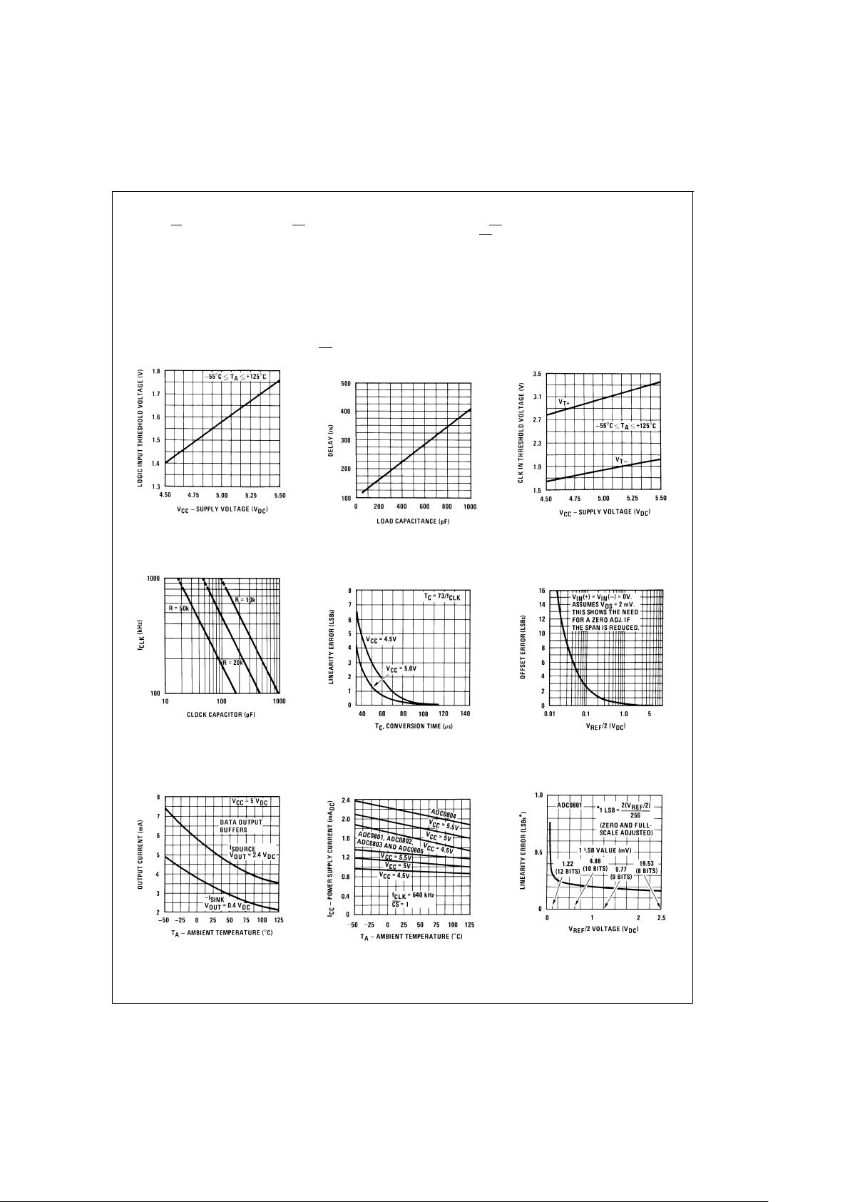
Typical Performance Characteristics
Logic Input Threshold Voltage
vs. Supply Voltage
DS005671-38
Delay From Falling Edge of
RD to Output Data Valid
vs. Load Capacitance
DS005671-39
CLK IN Schmitt Trip Levels
vs. Supply Voltage
DS005671-40
f
CLK
vs. Clock Capacitor
DS005671-41
Full-Scale Error vs
Conversion Time
DS005671-42
Effect of Unadjusted Offset Error
vs. V
REF
/2 Voltage
DS005671-43
Output Current vs
Temperature
DS005671-44
Power Supply Current
vs Temperature (Note 9)
DS005671-45
Linearity Error at Low
V
REF
/2 Voltages
DS005671-46
ADC0801/ADC0802/ADC0803/ADC0804/ADC0805
www.national.com5
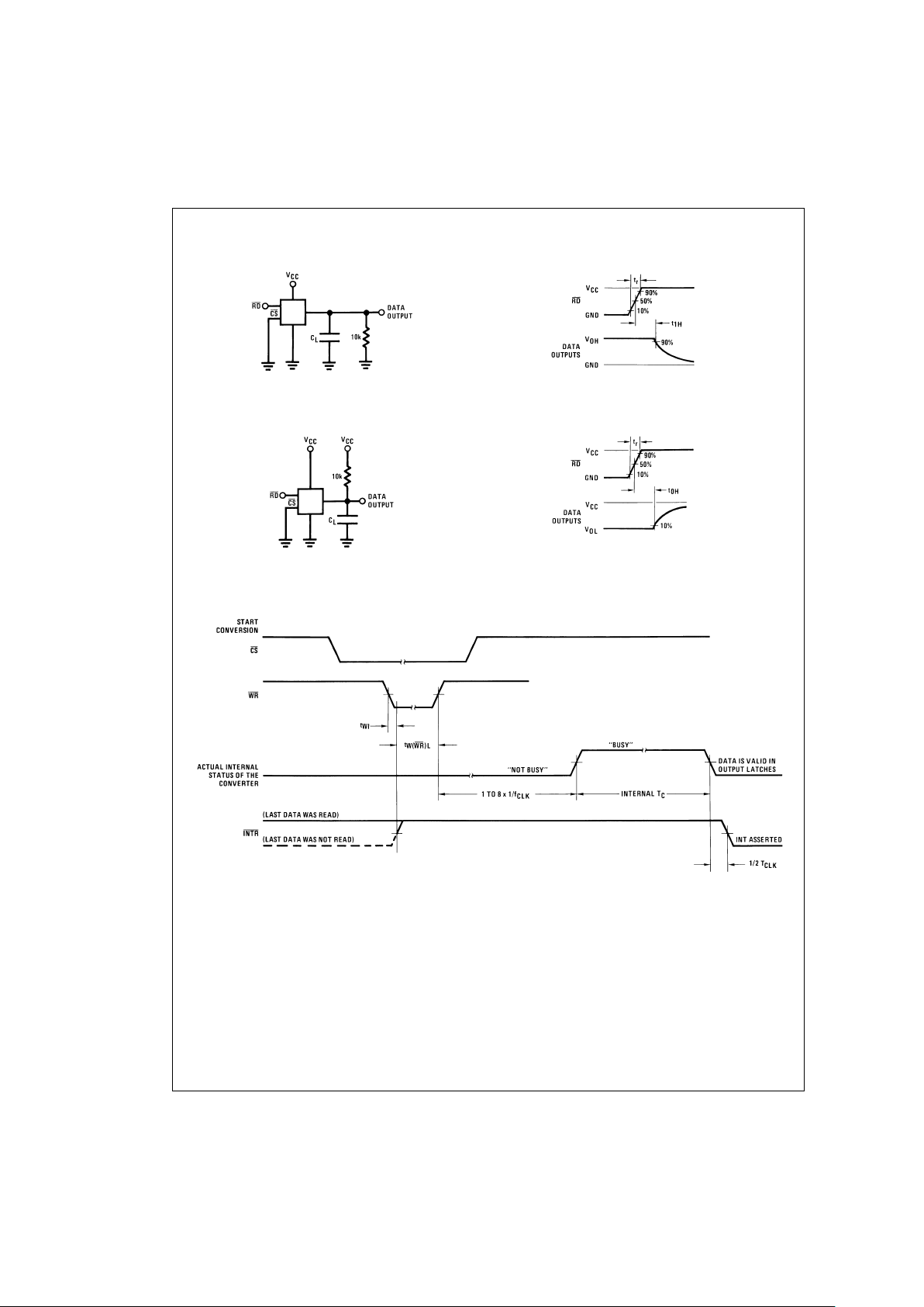
TRI-STATE Test Circuits and Waveforms
Timing Diagrams
(All timing is measured from the 50%voltage points)
t
1H
DS005671-47
t1H,C
L
=
10 pF
DS005671-48
t
r
=
20 ns
t
0H
DS005671-49
t0H,C
L
=
10 pF
DS005671-50
t
r
=
20 ns
DS005671-51
ADC0801/ADC0802/ADC0803/ADC0804/ADC0805
www.national.com 6
Timing Diagrams (All timing is measured from the 50
%
voltage points) (Continued)
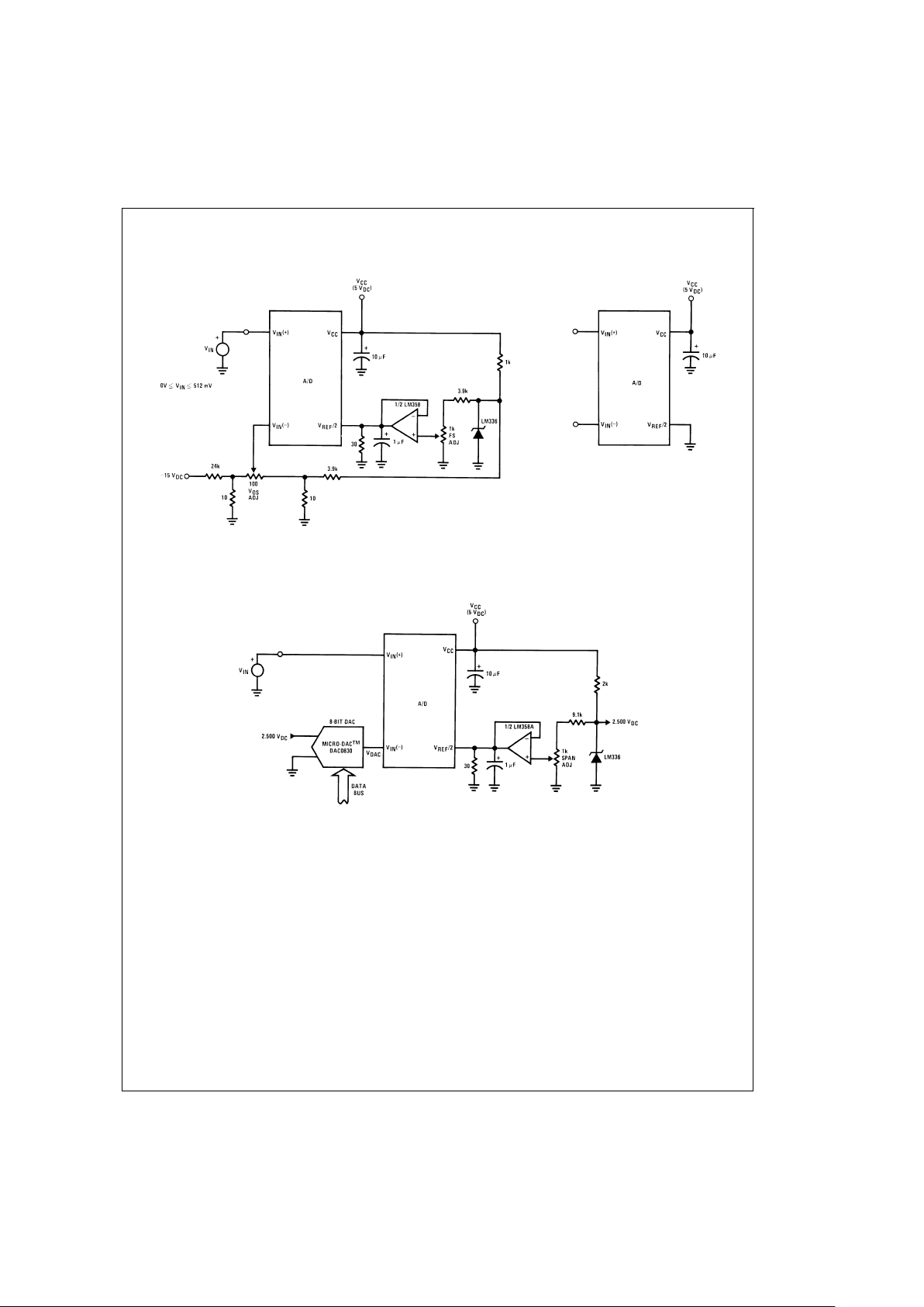
Typical Applications
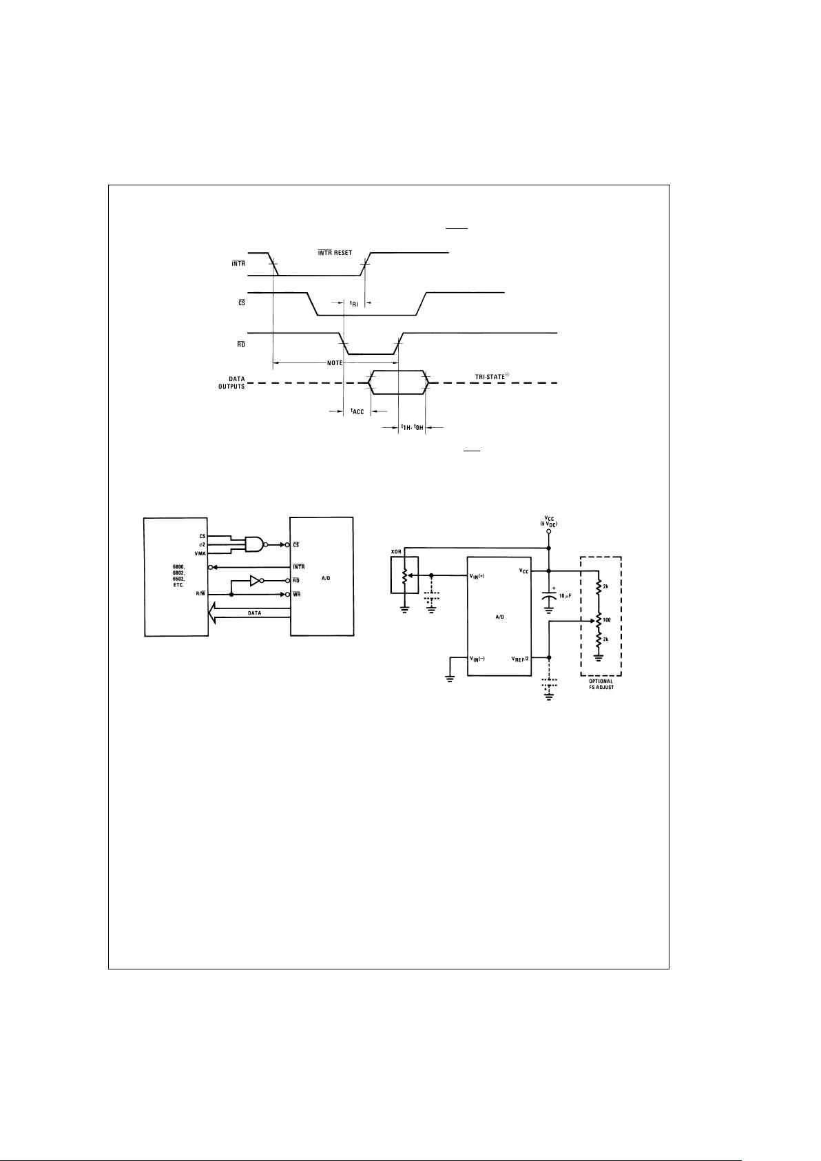
Output Enable and Reset with INTR
DS005671-52
Note: Read strobe must occur 8 clock periods (8/f
CLK
) after assertion of interrupt to guarantee reset of INTR .
6800 Interface
DS005671-53
Ratiometeric with Full-Scale Adjust
DS005671-54
Note: before using caps at VINor V
REF
/2,
see section 2.3.2 Input Bypass Capacitors.
ADC0801/ADC0802/ADC0803/ADC0804/ADC0805
www.national.com7
Typical Applications (Continued)
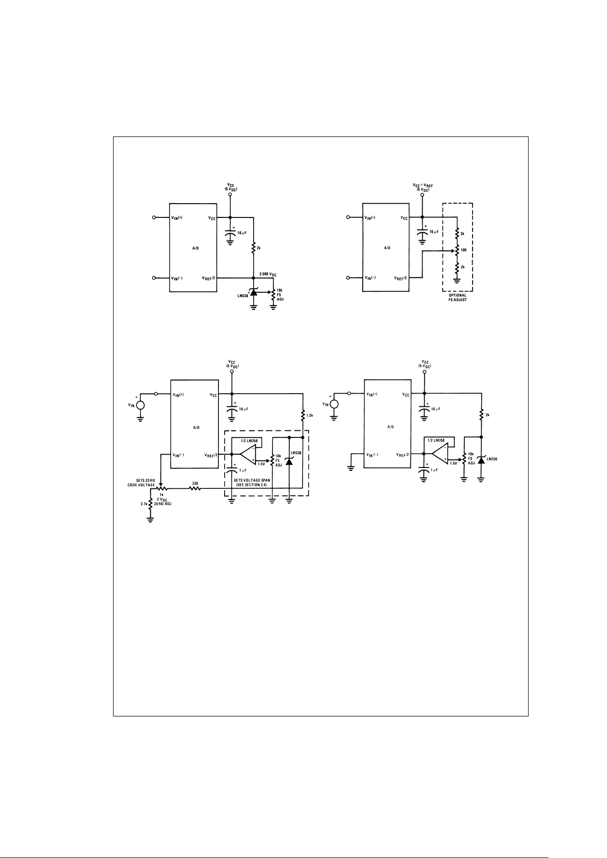
Absolute with a 2.500V Reference
DS005671-55
*For low power, see also LM385–2.5
Absolute with a 5V Reference
DS005671-56
Zero-Shift and Span Adjust: 2V ≤ VIN≤ 5V
DS005671-57
Span Adjust: 0V ≤ VIN≤ 3V
DS005671-58
ADC0801/ADC0802/ADC0803/ADC0804/ADC0805
www.national.com 8
Typical Applications (Continued)
Directly Converting a Low-Level Signal
DS005671-59
V
REF
/2=256 mV
A µP Interfaced Comparator
DS005671-60
For:
V
IN
(+)>VIN(−)
Output=FF
HEX
For:
V
IN
(+)<VIN(−)
Output=00
HEX
1 mV Resolution with µP Controlled Range
DS005671-61
V
REF
/2=128 mV
1 LSB=1mV
V
DAC≤VIN
≤(V
DAC
+256 mV)
0 ≤ V
DAC
<
2.5V
ADC0801/ADC0802/ADC0803/ADC0804/ADC0805
www.national.com9
Typical Applications (Continued)
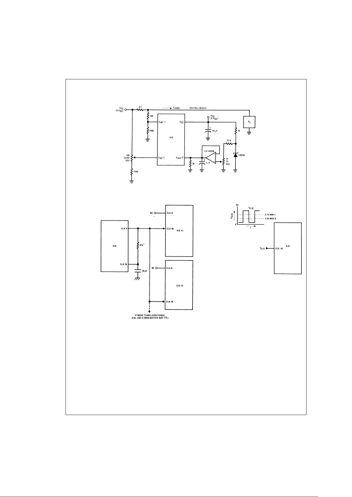
Digitizing a Current Flow
DS005671-62
Self-Clocking Multiple A/Ds
DS005671-63
* Use a large R value
to reduce loading
at CLK R output.
External Clocking
DS005671-64
100 kHz≤f
CLK
≤1460 kHz
ADC0801/ADC0802/ADC0803/ADC0804/ADC0805
www.national.com 10
Typical Applications (Continued)
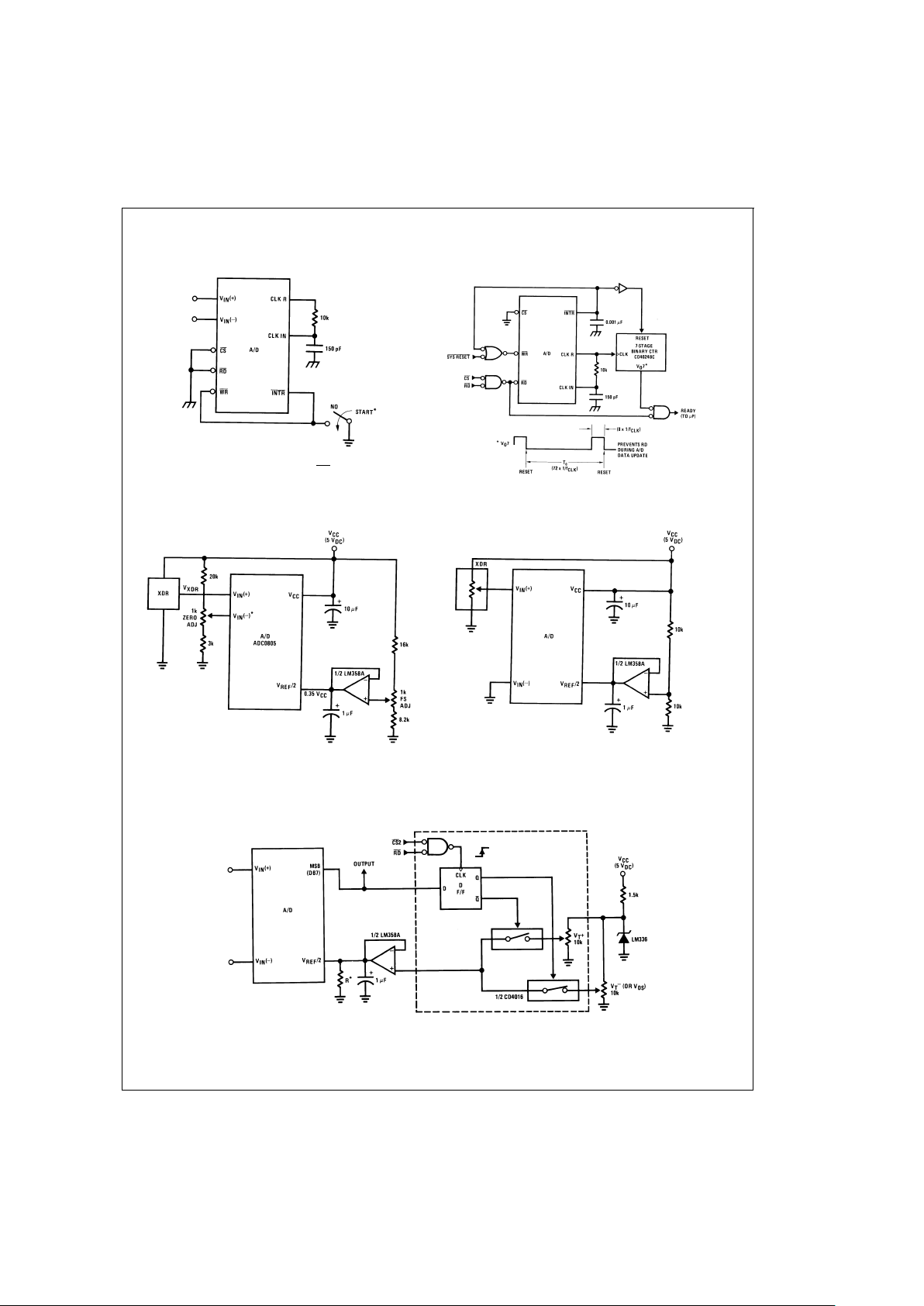
Self-Clocking in Free-Running Mode
DS005671-65
*After power-up, a momentary grounding of the WR input is needed to
guarantee operation.
µP Interface for Free-Running A/D
DS005671-66
Operating with “Automotive” Ratiometric Transducers
DS005671-67
*VIN(−)=0.15 V
CC
15%of VCC≤V
XDR
≤85%of V
CC
Ratiometric with V
REF
/2 Forced
DS005671-68
µP Compatible Differential-Input Comparator with Pre-Set VOS(with or without Hysteresis)
DS005671-69
*See
Figure 5
to select R value
DB7=“1” for V
IN
(+)>VIN(−)+(V
REF
/2)
Omit circuitry within the dotted area if
hysteresis is not needed
ADC0801/ADC0802/ADC0803/ADC0804/ADC0805
www.national.com11
Typical Applications (Continued)
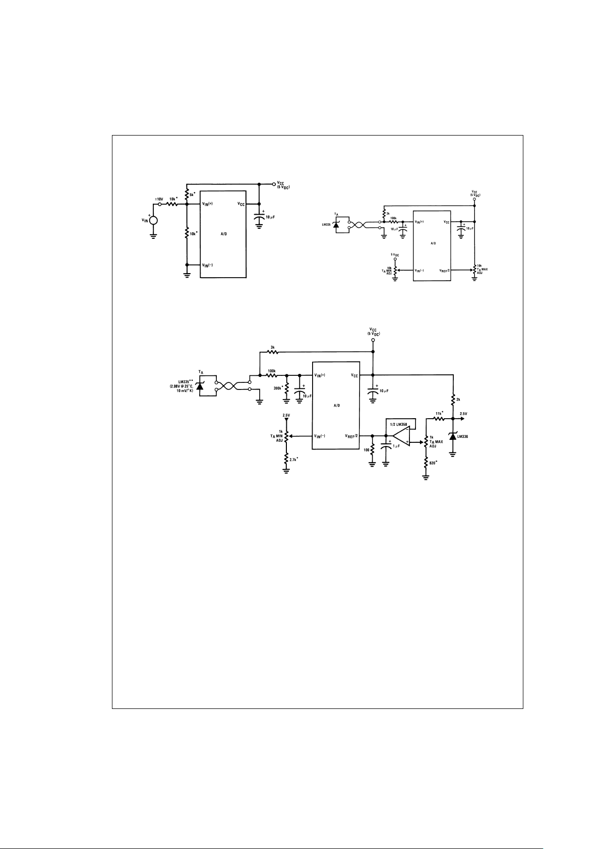
Handling
±
10V Analog Inputs
DS005671-70
*Beckman Instruments#694-3-R10K resistor array
Low-Cost, µP Interfaced, Temperature-to-Digital
Converter
DS005671-71
µP Interfaced Temperature-to-Digital Converter
DS005671-72
*Circuit values shown are for 0˚C≤TA≤+128˚C
**
*
Can calibrate each sensor to allow easy replacement, then A/D can be calibrated with a pre-set input voltage.
ADC0801/ADC0802/ADC0803/ADC0804/ADC0805
www.national.com 12
Typical Applications (Continued)
Handling
±
5V Analog Inputs
DS005671-33
*Beckman Instruments#694-3-R10K resistor array
Read-Only Interface
DS005671-34
µP Interfaced Comparator with Hysteresis
DS005671-35
Protecting the Input
DS005671-9
Diodes are 1N914
ADC0801/ADC0802/ADC0803/ADC0804/ADC0805
www.national.com13

Typical Applications (Continued)
Analog Self-Test for a System
DS005671-36
A Low-Cost, 3-Decade Logarithmic Converter
DS005671-37
*LM389 transistors
A, B, C, D=LM324A quad op amp
ADC0801/ADC0802/ADC0803/ADC0804/ADC0805
www.national.com 14

Typical Applications (Continued)
3-Decade Logarithmic A/D Converter
DS005671-73
Noise Filtering the Analog Input
DS005671-74
f
C
=
20 Hz
Uses Chebyshev implementation for steeper roll-off unity-gain, 2nd order,
low-pass filter
Adding a separate filter for each channel increases system response time
if an analog multiplexer is used
Multiplexing Differential Inputs
DS005671-75
Output Buffers with A/D Data Enabled
DS005671-76
*A/D output data is updated 1 CLK period prior to assertion of INTR
Increasing Bus Drive and/or Reducing Time on Bus
DS005671-77
*Allows output data to set-up at falling edge of CS
ADC0801/ADC0802/ADC0803/ADC0804/ADC0805
www.national.com15

Typical Applications (Continued)
Functional Description
1.0 UNDERSTANDING A/D ERROR SPECS
A perfect A/D transfer characteristic (staircase waveform) is
shown in
Figure 1
. The horizontal scale is analog input voltage and the particular points labeled are in steps of 1 LSB
(19.53 mV with 2.5V tied to the V
REF
/2 pin). The digital output codes that correspond to these inputs are shownas D−1,
D, and D+1. For the perfect A/D, not only will center-value
(A−1, A, A+1, ....)analog inputs produce the correct out-
put digital codes, butalso each riser (the transitions between
adjacent output codes) will be located
±
1
⁄2LSB away from
each center-value. As shown, the risers are ideal and have
no width. Correct digital output codes will be provided for a
range of analog input voltages that extend
±
1
⁄2LSB from the
ideal center-values. Each tread (the range of analog input
voltage that provides the same digital output code) is therefore 1 LSB wide.
Sampling an AC Input Signal
DS005671-78
Note 11: Oversample whenever possible [keep fs>2f(−60)] to eliminate input frequency folding (aliasing) and to allow for the skirt response of the filter.
Note 12: Consider the amplitude errors which are introduced within the passband of the filter.
70%Power Savings by Clock Gating
DS005671-79
(Complete shutdown takes ≈ 30 seconds.)
Power Savings by A/D and V
REF
Shutdown
DS005671-80
*Use ADC0801, 02, 03 or 05 for lowest power consumption.
Note: Logic inputs can be driven to V
CC
with A/D supply at zero volts.
Buffer prevents data bus from overdriving output of A/D when in shutdown mode.
ADC0801/ADC0802/ADC0803/ADC0804/ADC0805
www.national.com 16

Functional Description (Continued)
Figure 2
shows a worst case error plot for theADC0801. All
center-valued inputs are guaranteed to produce the correct
output codes and the adjacent risers are guaranteed to be
no closer to the center-value points than
±
1
⁄4LSB. In other
words, if we apply an analog input equal to the center-value
±
1
⁄4LSB,
we guarantee
that theA/D will produce the correct
digital code. The maximum range of the position of the code
transition is indicated by the horizontal arrow and it is guaranteed to be no more than
1
⁄2LSB.
The error curve of
Figure 3
shows a worst case error plot for
the ADC0802. Here we guarantee that if we apply an analog
input equal to the LSB analog voltage center-value the A/D
will produce the correct digital code.
Next to each transfer function is shown the corresponding
error plot.Many people may be more familiar with error plots
than transfer functions. The analog input voltage to the A/D
is provided by either a linear ramp or by the discrete output
steps of a high resolution DAC. Notice that the error is continuously displayed and includes the quantization uncertainty
of the A/D. For example the error at point 1 of
Figure 1
is +1⁄
2
LSB because the digital code appeared1⁄2LSB in advance
of the center-value of the tread. The error plots always have
a constant negative slope and the abrupt upside steps are
always 1 LSB in magnitude.
Transfer Function
DS005671-81
Error Plot
DS005671-82
FIGURE 1. Clarifying the Error Specs of an A/D Converter
Accuracy
=
±
0 LSB: A Perfect A/D
Transfer Function
DS005671-83
Error Plot
DS005671-84
FIGURE 2. Clarifying the Error Specs of an A/D Converter
Accuracy
=
±
1
⁄4LSB
ADC0801/ADC0802/ADC0803/ADC0804/ADC0805
www.national.com17

Functional Description (Continued)
2.0 FUNCTIONAL DESCRIPTION
The ADC0801 series contains a circuit equivalent of the
256R network. Analog switches are sequenced by successive approximation logic tomatch theanalog differenceinput
voltage [V
IN
(+)−VIN(−)] to a correspondingtap on the R network. The most significant bit is tested first and after 8 comparisons (64 clock cycles) a digital 8-bit binary code (1111
1111=full-scale) is transferred to an output latch and then
an interrupt is asserted (INTR makes a high-to-low transition).A conversion in process can be interrupted by issuing a
second start command. The device may be operated in the
free-running mode by connecting INTR to the WR input with
CS=0. To ensure start-up under all possible conditions, an
external WR pulse is required during the first power-up
cycle.
On the high-to-low transition of the WR input the internal
SAR latches and the shift register stages are reset. As long
as the CS input and WR input remain low,theA/D will remain
in a reset state.
Conversion will start from 1 to 8 clock periods after at least one of these inputs makes a low-to-high
transition
.
A functional diagram of theA/D converter is shown in
Figure
4
. All of the package pinouts are shown and the major logic
control paths are drawn in heavier weight lines.
The converter is started by having CS and WR simulta-
neously low. This sets the start flip-flop (F/F) and the resulting “1” level resets the 8-bit shift register,resets the Interrupt
(INTR) F/F and inputs a “1” tothe Dflop, F/F1,which is at the
input end of the8-bit shift register. Internalclock signals then
transfer this “1” to the Q output of F/F1. The AND gate, G1,
combines this “1” output with a clock signal to provide a reset
signal to the start F/F. If the set signal is no longer present
(either WR or CS is a “1”) the start F/F is reset and the 8-bit
shift register then can have the “1” clocked in, which starts
the conversion process. If the set signal were to still be
present, this reset pulse would have no effect (both outputs
of the start F/F would momentarily be at a “1” level) and the
8-bit shift register would continue to be held in the reset
mode. This logic therefore allows for wide CS and WR signals and the converter will start after at least one of these
signals returns high and the internal clocks again provide a
reset signal for the start F/F.
Transfer Function
DS005671-85
Error Plot
DS005671-86
FIGURE 3. Clarifying the Error Specs of an A/D Converter
Accuracy
=
±
1
⁄2LSB
ADC0801/ADC0802/ADC0803/ADC0804/ADC0805
www.national.com 18

Functional Description (Continued)
After the “1” is clocked through the 8-bit shift register (which
completes the SAR search) it appears as the input to the
D-type latch, LATCH 1. As soon as this “1” is output from the
shift register, theAND gate, G2, causes the new digital word
to transfer to the TRI-STATE output latches. When LATCH 1
is subsequently enabled, the Q output makes a high-to-low
transition which causes the INTR F/F to set. An inverting
buffer then supplies the INTR input signal.
Note that this SET control of the INTR F/F remains low for 8
of the external clock periods (as the internal clocks run at1⁄
8
of the frequency of the external clock). If the data output is
continuously enabled (CS and RD both held low), the INTR
output will still signal the end of conversion (by a high-to-low
transition), because the SET input can control the Q output
of the INTR F/F even though the RESET input is constantly
at a “1” level in this operating mode. This INTR output will
therefore stay low forthe duration of the SET signal, which is
8 periods of the external clock frequency (assuming the A/D
is not started during this interval).
When operating in the free-running or continuous conversion
mode (INTR pin tied to WR and CS wired low — see also
section 2.8), the START F/F is SET by the high-to-low transition of the INTR signal. This resets the SHIFT REGISTER
which causes the input to the D-type latch, LATCH 1, to go
low.As the latch enable input is still present, the Qoutput will
go high, which then allows the INTR F/F to be RESET. This
reduces the width of the resulting INTR output pulse to only
a few propagation delays (approximately 300 ns).
When data is tobe read, the combination of both CSand RD
being low will cause the INTR F/F to be reset and the
TRI-STATE output latches will be enabled to providethe 8-bit
digital outputs.
2.1 Digital Control Inputs
The digital control inputs (CS, RD, and WR) meet standard
T2L logic voltage levels. These signals have been renamed
when compared to the standardA/D Start and Output Enable
labels. In addition, these inputs are active low to allow an
easy interface to microprocessor control busses. For
non-microprocessor based applications, the CS input (pin 1)
can be grounded and the standard A/D Start function is obtained by an active low pulse applied at the WR input (pin 3)
and the Output Enable function is caused by an active low
pulse at the RD input (pin 2).
DS005671-13
Note 13: CS shown twice for clarity.
Note 14: SAR=Successive Approximation Register.
FIGURE 4. Block Diagram
ADC0801/ADC0802/ADC0803/ADC0804/ADC0805
www.national.com19

Functional Description (Continued)
2.2 Analog Differential Voltage Inputs and
Common-Mode Rejection
ThisA/D hasadditional applications flexibility due to the analog differential voltage input. The V
IN
(−) input (pin 7) can be
used to automatically subtract a fixed voltage value from the
input reading (tare correction). Thisis alsouseful in 4 mA–20
mA current loop conversion. In addition, common-mode
noise can be reduced by use of the differential input.
The time interval between sampling V
IN
(+) and VIN(−) is 4-1⁄
2
clock periods. The maximum error voltage due to this slight
time difference between the input voltage samples is given
by:
where:
∆V
e
is the error voltage due to sampling delay
V
P
is the peak value of the common-mode voltage
f
cm
is the common-mode frequency
As an example, to keep this error to
1
⁄4LSB (∼5 mV) when
operating with a 60 Hz common-mode frequency, f
cm
, and
using a640 kHzA/D clock, f
CLK
, wouldallow a peak value of
the common-mode voltage, V
P
, which is given by:
or
which gives
V
P
≅
1.9V.
The allowed range of analog input voltages usually places
more severe restrictions on input common-mode noise levels.
An analog input voltage with a reduced span and a relatively
large zero offset can be handled easily by making use of the
differential input (see section 2.4 Reference Voltage).
2.3 Analog Inputs
2.3 1 Input Current
Normal Mode
Due to the internal switching action, displacement currents
will flow at the analog inputs.This is due to on-chip stray capacitance to ground as shown in
Figure 5
.
The voltage on this capacitance is switched and will result in
currents entering the V
IN
(+) input pin and leaving the VIN(−)
input which will depend on the analog differential input voltage levels. These current transients occur at the leading
edge of the internal clocks. They rapidly decay and
do not
cause errors
as the on-chip comparator is strobed atthe end
of the clock period.
Fault Mode
If the voltage source applied to the V
IN
(+) or VIN(−) pin ex-
ceeds the allowed operating range of V
CC
+50 mV, large in-
put currents can flow through a parasitic diode to the V
CC
pin. If these currents can exceed the 1 mA max allowed
spec, an external diode (1N914) should be added to bypass
this current to the V
CC
pin (with the current bypassed with
this diode, the voltage at the V
IN
(+) pin can exceed the V
CC
voltage by the forward voltage of this diode).
2.3.2 Input Bypass Capacitors
Bypass capacitors at the inputs will average these charges
and cause a DC current to flow through the output resistances of the analog signal sources. This charge pumping
action is worse for continuous conversionswith theV
IN
(+) input voltage at full-scale. For continuous conversions with a
640 kHz clock frequency with the V
IN
(+) input at 5V, this DC
current is at a maximum of approximately 5 µA. Therefore,
bypass capacitors should notbe used at the analog inputs or
the V
REF
/2 pin
for high resistance sources (>1kΩ). If input
bypass capacitors are necessary for noise filtering and high
source resistance is desirable to minimizecapacitor size,the
detrimental effects of the voltage drop across this inputresistance, whichis due to the average value of the input current,
can be eliminated with a full-scale adjustment while the
given source resistor and input bypass capacitor are both in
place. This is possible because the average value of the input current is a precise linear function of the differential input
voltage.
2.3.3 Input Source Resistance
Large values of source resistance where an input bypass capacitor is not used,
will not cause errors
as the input currents
settle out prior to the comparison time. If a low pass filter is
required in the system, use a low valued series resistor
(≤ 1kΩ) for a passive RC section or add an op amp RC ac-
tive low pass filter. For low source resistance applications,
(≤ 1kΩ), a 0.1 µF bypass capacitor at the inputs will prevent
noise pickup due to series lead inductance of a long wire. A
DS005671-14
rONof SW 1 and SW 2≅5kΩ
r=r
ONCSTRAY
≅
5kΩx12pF=60 ns
FIGURE 5. Analog Input Impedance
ADC0801/ADC0802/ADC0803/ADC0804/ADC0805
www.national.com 20

Functional Description (Continued)
100Ω series resistor can be used to isolate this
capacitor—both the R and C are placed outside the feedback loop— from the output of an op amp, if used.
2.3.4 Noise
The leads to the analog inputs (pins 6 and 7) should be kept
as short as possible to minimize input noise coupling. Both
noise and undesired digital clock coupling to these inputs
can cause system errors.The sourceresistance for these inputs should, in general,be kept below 5 kΩ. Larger values of
source resistance can cause undesired system noise
pickup. Input bypass capacitors, placed from the analog inputs to ground, will eliminate system noise pickup but can
create analog scale errors as these capacitors will average
the transient input switching currents of the A/D (see section
2.3.1.). This scale error depends on both a large source resistance and the use of an input bypass capacitor. This error
can be eliminated by doing a full-scaleadjustment of the A/D
(adjust V
REF
/2 for a proper full-scale reading — see section
2.5.2 on Full-Scale Adjustment) with the source resistance
and input bypass capacitor in place.
2.4 Reference Voltage
2.4.1 Span Adjust
For maximum applications flexibility, these A/Ds have been
designed to accommodatea5V
DC
, 2.5 VDCor an adjusted
voltage reference. This has been achieved in the design of
the IC as shown in
Figure 6
.
Notice that the reference voltage for the IC is either
1
⁄2of the
voltage applied to the V
CC
supply pin, or is equal to the volt-
age that is externallyforced at the V
REF
/2 pin. This allows for
a ratiometric voltage reference using the V
CC
supply, a 5
V
DC
reference voltage can be used for the VCCsupply or a
voltage less than 2.5 V
DC
can be applied to the V
REF
/2 input
for increased application flexibility. The internal gain to the
V
REF
/2 input is 2, making the full-scale differential input volt-
age twice the voltage at pin 9.
An example of the use of an adjusted reference voltage is to
accommodate a reduced span— or dynamic voltage range
of the analog input voltage. If the analog input voltage were
to range from 0.5 V
DC
to 3.5 VDC, instead of 0V to 5 VDC, the
span would be 3V as shown in
Figure 7
. With 0.5 VDCap-
plied to the V
IN
(−) pin to absorb the offset,the referencevolt-
age can be made equal to
1
⁄2of the 3V span or 1.5 VDC. The
A/D now will encodethe V
IN
(+) signal from 0.5Vto 3.5 V with
the 0.5V input corresponding to zero and the 3.5 V
DC
input
corresponding to full-scale. The full 8 bits of resolution are
therefore applied over this reduced analog input voltage
range.
2.4.2 Reference Accuracy Requirements
The converter can be operated in a ratiometric mode or an
absolute mode. In ratiometric converter applications, the
magnitude of the reference voltage is a factor in both the output of the source transducer and the output of the A/D converter and therefore cancels out in the final digital output
code. The ADC0805 is specified particularly for use in ratiometric applications with noadjustments required. In absolute
conversion applications, both the initial value and the temperature stability of the reference voltage are important factors in the accuracy of the A/D converter. For V
REF
/2 volt-
ages of 2.4 V
DC
nominal value, initial errors of±10 mVDCwill
cause conversion errors of
±
1 LSB due to the gain of2 ofthe
V
REF
/2 input. In reduced span applications, the initial value
and the stability of the V
REF
/2 input voltage become even
more important. For example, if the span is reduced to 2.5V,
the analog input LSB voltage value is correspondingly reduced from 20 mV (5V span) to 10 mV and 1 LSB at the
V
REF
/2 input becomes 5 mV. As can be seen, this reduces
the allowed initial tolerance of the reference voltage and requires correspondingly less absolute change with temperature variations. Note that spans smaller than 2.5V place
even tighter requirements on the initial accuracy and stability
of the reference source.
In general, the magnitude of the reference voltage will require an initial adjustment. Errors due to an improper value
of reference voltage appear as full-scale errors in the A/D
transfer function. IC voltage regulators may be used for references if the ambient temperature changes are not excessive. The LM336B 2.5V IC reference diode (from National
Semiconductor) has a temperature stability of 1.8 mV typ
(6 mV max) over 0˚C≤T
A
≤+70˚C. Other temperature range
parts are also available.
DS005671-15
FIGURE 6. The V
REFERENCE
Design on the IC
ADC0801/ADC0802/ADC0803/ADC0804/ADC0805
www.national.com21

Functional Description (Continued)
2.5 Errors and Reference Voltage Adjustments
2.5.1 Zero Error
The zero of the A/D does not require adjustment. If the minimum analog input voltage value, V
IN(MIN)
, is not ground, a
zero offset can be done. The converter can be made to output 0000 0000 digital code for this minimum input voltage by
biasing theA/D V
IN
(−) input at this V
IN(MIN)
value (see Applications section). This utilizes the differential mode operation
of the A/D.
The zero error of the A/D converter relates to the location of
the first riser of the transfer function and can be measured by
grounding the V
IN
(−) input and applying a small magnitude
positive voltage to the V
IN
(+) input. Zero error is the difference between the actual DC input voltage that is necessary
to just cause an output digital codetransition from0000 0000
to 0000 0001 and the ideal
1
⁄2LSB value (1⁄2LSB=9.8 mV
for V
REF
/2=2.500 VDC).
2.5.2 Full-Scale
The full-scale adjustment can be made by applying a differential input voltage that is 1
1
⁄2LSB less than the desired analog full-scale voltage range and then adjusting the magnitude of the V
REF
/2 input (pin 9 or the VCCsupply if pin 9 is
not used) for a digital output code that is just changing from
1111 1110 to 1111 1111.
2.5.3 Adjusting for an Arbitrary Analog Input Voltage
Range
If the analog zero voltage of the A/D is shifted away from
ground (for example, to accommodate an analog input signal
that does not go to ground) this new zero reference should
be properly adjusted first. A V
IN
(+) voltage that equals this
desired zero reference plus
1
⁄2LSB (where the LSB is calcu-
lated for the desired analog span, 1 LSB=analog span/256)
is applied to pin 6 and the zero reference voltage at pin 7
should then be adjusted to just obtain the 00
HEX
to 01
HEX
code transition.
The full-scale adjustment should then be made (with the
proper V
IN
(−) voltage applied) by forcing a voltage to the
V
IN
(+) input which is given by:
where:
V
MAX
=
The high end of the analog input range
and
V
MIN
=
the low end (the offset zero) of the analog range.
(Both are ground referenced.)
The V
REF
/2 (or VCC) voltage is then adjusted to provide a
code change from FE
HEX
to FF
HEX
. This completes the ad-
justment procedure.
2.6 Clocking Option
The clock for the A/D can be derived from the CPU clock or
an external RC can be added to provide self-clocking. The
CLK IN (pin 4) makes use of a Schmitt trigger as shown in
Figure 8
.
DS005671-87
a) Analog Input Signal Example
DS005671-88
*
Add if V
REF
/2 ≤ 1VDCwith LM358 to draw 3 mA to ground.
b) Accommodating an Analog Input from
0.5V (Digital Out=00
HEX
) to 3.5V
(Digital Out=FF
HEX
)
FIGURE 7. Adapting the A/D Analog Input Voltages to Match an Arbitrary Input Signal Range
ADC0801/ADC0802/ADC0803/ADC0804/ADC0805
www.national.com 22

Functional Description (Continued)
Heavy capacitive or DC loading of the clock R pin should be
avoided as this will disturb normal converter operation.
Loads less than 50 pF, such as driving up to 7 A/D converter
clock inputs from a single clock R pin of 1 converter, are allowed. For larger clock line loading, a CMOS or low power
TTL buffer or PNP input logic should be used tominimize the
loading on the clock R pin (do not use a standard TTL
buffer).
2.7 Restart During a Conversion
If the A/D is restarted (CS and WR go low and return high)
during a conversion, the converter is reset and a new conversion is started. The output data latch is not updated if the
conversion in process is not allowed to be completed, therefore the data of the previous conversion remains in this latch.
The INTR output simply remains at the “1” level.
2.8 Continuous Conversions
For operation in the free-running mode an initializing pulse
should be used, following power-up, to ensure circuit operation. In this application, the CS input is grounded and the WR
input is tied to the INTR output. This WR and INTR node
should be momentarily forced to logic low following a
power-up cycle to guarantee operation.
2.9 Driving the Data Bus
This MOS A/D, like MOS microprocessors and memories,
will require a bus driver when the total capacitance of the
data bus gets large. Other circuitry, which is tied to the data
bus, will add to the total capacitive loading, even in
TRI-STATE (high impedance mode). Backplane bussing
also greatly adds to the stray capacitance of the data bus.
There are some alternatives available to the designer to
handle this problem. Basically, the capacitive loading of the
data bus slows down the response time, even though DC
specifications are still met. For systems operating with a
relatively slow CPU clock frequency, more time is available
in which to establish properlogic levelson thebus and therefore higher capacitive loads can be driven (see typical characteristics curves).
At higher CPU clock frequencies time can be extended for
I/O reads (and/or writes) by inserting wait states (8080) or
using clock extending circuits (6800).
Finally,if time is short and capacitive loading is high,external
bus drivers must be used. These can be TRI-STATE buffers
(low power Schottky such as the DM74LS240 series is recommended) or special higher drive current products which
are designedas bus drivers. High current bipolar bus drivers
with PNP inputs are recommended.
2.10 Power Supplies
Noise spikes on the V
CC
supply line can cause conversion
errors as the comparator will respond to this noise.A low inductance tantalum filter capacitor should be used close to
the converter V
CC
pin and values of 1 µF or greater are recommended. If an unregulated voltage is available in the system, a separate LM340LAZ-5.0, TO-92, 5V voltage regulator
for the converter (and other analog circuitry) will greatly reduce digital noise on the V
CC
supply.
2.11 Wiring and Hook-Up Precautions
Standard digital wire wrap sockets are not satisfactory for
breadboarding this A/D converter. Sockets on PC boards
can be used and all logic signal wires and leads should be
grouped and kept as far away as possible from the analog
signal leads. Exposed leads to the analog inputs can cause
undesired digital noise and hum pickup, therefore shielded
leads may be necessary in many applications.
A single point analog ground that is separate from the logic
ground points should be used. The power supply bypass capacitor and the self-clocking capacitor (if used) should both
be returned to digital ground.Any V
REF
/2 bypass capacitors,
analog input filter capacitors, or input signal shielding should
be returned to the analog ground point. A test for proper
grounding is to measure the zero error of the A/D converter.
Zero errors in excess of
1
⁄4LSB can usually be traced to improper board layout and wiring (see section 2.5.1 for measuring the zero error).
3.0 TESTING THE A/D CONVERTER
There are many degrees of complexity associated with testing an A/D converter. One of the simplest tests is to apply a
known analog input voltage to the converterand useLEDs to
display the resulting digital output code asshown in
Figure 9
.
For ease of testing, the V
REF
/2 (pin 9) should be supplied
with 2.560 V
DC
andaVCCsupply voltage of 5.12 VDCshould
be used. This provides an LSB value of 20 mV.
If a full-scale adjustment is to be made, an analog input volt-
age of 5.090 V
DC
(5.120–11⁄2LSB) should be applied to the
V
IN
(+) pin with the VIN(−) pin grounded. The value of the
V
REF
/2 input voltage should then be adjusted until the digital
output code is just changing from 1111 1110 to 1111 1111.
This value of V
REF
/2 should then be used for all the tests.
The digital output LED display can be decoded by dividing
the 8 bits into 2 hex characters, the 4 most significant (MS)
and the 4 least significant (LS).
Table1
shows the fractional
binary equivalent of these two 4-bit groups. By adding the
voltages obtained from the “VMS” and “VLS” columns in
Table 1
, the nominal value of the digital display (when
V
REF
/2=2.560V) can be determined. For example, for an
output LED display of 1011 0110 or B6 (in hex), the voltage
values from the table are 3.520 + 0.120 or 3.640 V
DC
. These
voltage values represent the center-values of a perfect A/D
converter. The effects of quantization error have to be accounted for in the interpretation of the test results.
DS005671-17
FIGURE 8. Self-Clocking the A/D
ADC0801/ADC0802/ADC0803/ADC0804/ADC0805
www.national.com23

Functional Description (Continued)
For a higher speed test system, or to obtain plotted data, a
digital-to-analog converter is needed for the test set-up. An
accurate 10-bit DAC can serve as the precision voltage
source for the A/D. Errors of the A/D under test can be expressed as either analog voltages or differences in 2 digital
words.
Abasic A/D tester thatuses a DAC and providesthe error as
an analog output voltage is shown in
Figure 8
.The2op
amps can be eliminated if a lab DVM with a numerical subtraction feature is available to read the difference voltage,
“A–C”, directly. The analog input voltage can be supplied by
a low frequency ramp generator and an X-Y plotter can be
used to provide analog error (Y axis) versus analog input (X
axis).
For operation with a microprocessor or a computer-based
test system, it is more convenient to present the errors digitally.This can be done with the circuit of
Figure 11
, where the
output code transitions can be detected as the 10-bit DAC is
incremented. This provides
1
⁄4LSB steps for the 8-bitA/D under test. If the results of this test are automatically plotted
with the analog input on the X axis and the error (in LSB’s)
as the Y axis, a useful transfer function of the A/D under test
results. For acceptance testing, the plot is not necessary and
the testing speed can be increased by establishing internal
limits on the allowed error for each code.
4.0 MICROPROCESSOR INTERFACING
To dicuss the interface with 8080A and 6800 microprocessors, a common sample subroutine structure is used. The
microprocessor starts the A/D, reads and stores the results
of 16 successive conversions, then returns to the user’s program. The 16 data bytes are stored in 16 successive
memory locations. All Data and Addresses will be given in
hexadecimal form. Software and hardware details are provided separately for each type of microprocessor.
4.1 Interfacing 8080 Microprocessor Derivatives (8048,
8085)
This converter has been designed to directly interface with
derivatives of the 8080 microprocessor. The A/D can be
mapped into memory space (using standard memory address decoding for CS and the MEMR and MEMW strobes)
or it can be controlled as an I/O device by using the I/O R
and I/O W strobes and decoding the address bits A0→A7
(or address bitsA8→A15 as they willcontain thesame 8-bit
address information) to obtain the CS input. Using the I/O
space provides 256 additional addresses and may allow a
simpler 8-bit address decoder but the data can only be input
to the accumulator. To make use of the additional memory
reference instructions, the A/D should be mapped into
memory space.An example of an A/D in I/O space is shown
in
Figure 12
.
DS005671-18
FIGURE 9. Basic A/D Tester
ADC0801/ADC0802/ADC0803/ADC0804/ADC0805
www.national.com 24

Functional Description (Continued)
TABLE 1. DECODING THE DIGITAL OUTPUT LEDs
OUTPUT VOLTAGE
FRACTIONAL BINARY VALUE FOR CENTER VALUES
HEX BINARY WITH
V
REF
/2=2.560 V
DC
MS GROUP LS GROUP VMS
GROUP
(Note 15)
VLS
GROUP
(Note 15)
F 1111 15/16 15/256 4.800 0.300
E 1110 7/8 7/128 4.480 0.280
D 1101 13/16 13/256 4.160 0.260
C 1100 3/4 3/64 3.840 0.240
B 1011 11/16 11/256 3.520 0.220
A 1010 5/8 5/128 3.200 0.200
9 1001 9/16 9/256 2.880 0.180
8 10001/2 1/32 2.560 0.160
7 0111 7/16 7/256 2.240 0.140
6 0110 3/8 3/128 1.920 0.120
5 0101 5/16 2/256 1.600 0.100
4 0100 1/4 1/64 1.280 0.080
3 0011 3/16 3/256 0.960 0.060
2 0010 1/8 1/128 0.640 0.040
1 0001 1/16 1/256 0.320 0.020
0 0000 00
Note 15: Display Output=VMS Group + VLS Group
DS005671-89
FIGURE 10. A/D Tester with Analog Error Output
DS005671-90
FIGURE 11. Basic “Digital” A/D Tester
ADC0801/ADC0802/ADC0803/ADC0804/ADC0805
www.national.com25

Functional Description (Continued)
DS005671-20
Note 16:*Pin numbers for the DP8228 system controller, others are INS8080A.
Note 17: Pin 23 of the INS8228 must be tied to +12V througha1kΩresistor to generate the RST 7
instruction when an interrupt is acknowledged as required by the accompanying sample program.
FIGURE 12. ADC0801_INS8080A CPU Interface
ADC0801/ADC0802/ADC0803/ADC0804/ADC0805
www.national.com 26

Functional Description (Continued)
Note 18: The stack pointer must be dimensioned because a RST 7 instruction pushes the PC onto the stack.
Note 19: All address used were arbitrarily chosen.
The standard control bus signals of the 8080 CS, RD and
WR) can be directly wired to the digital control inputs of the
A/D and the bus timing requirements are met to allow both
starting the converter and outputting the data onto the data
bus. A bus driver should be used for larger microprocessor
systems where the data bus leaves the PC board and/or
must drive capacitive loads larger than 100 pF.
4.1.1 Sample 8080A CPU Interfacing Circuitry and
Program
The following sample program and associated hardware
shown in
Figure 12
may be used to input data from the converter to the INS8080A CPU chip set (comprised of the
INS8080A microprocessor, the INS8228 system controller
and the INS8224 clock generator). For simplicity, the A/D is
controlled as an I/O device, specifically an 8-bit bi-directional
port located at an arbitrarily chosen port address, E0. The
TRI-STATE output capability of the A/D eliminates the need
for a peripheral interface device, however address decoding
is still required to generate the appropriate CS for the converter.
It is important to note that in systems where the A/D converter is 1-of-8 or less I/O mapped devices, no address decoding circuitry is necessary. Each of the 8 address bits (A0
to A7) can be directly used as CS inputs—one for each I/O
device.
4.1.2 INS8048 Interface
The INS8048 interface technique with the ADC0801 series
(see
Figure 13
) is simpler than the 8080A CPU interface.
There are 24 I/O lines and three test input lines in the 8048.
With these extra I/O lines available, one of the I/O lines (bit
0 of port 1) is used as the chip select signal to the A/D, thus
eliminating the use ofan external address decoder.Bus control signals RD, WR and INT of the 8048 are tied directly to
the A/D. The 16 converted data words are stored at on-chip
RAM locations from 20 to 2F (Hex). The RD and WR signals
are generated by reading from and writing into a dummy address, respectively. A sample interface program is shown
below.
SAMPLE PROGRAM FOR
Figure 12
ADC0801–INS8080A CPU INTERFACE
DS005671-99
ADC0801/ADC0802/ADC0803/ADC0804/ADC0805
www.national.com27

Functional Description (Continued)
4.2 Interfacing the Z-80
The Z-80 control bus is slightly different from that of the
8080. General RD and WR strobes are provided and separate memory request, MREQ, and I/O request, IORQ, signals are used which have to be combined with the generalized strobes to provide the equivalent 8080 signals. An
advantage of operating the A/D in I/O space with the Z-80 is
that the CPU will automatically insert one wait state (the RD
and WR strobes are extended one clock period) to allow
more time for the I/O devices to respond. Logic to map the
A/D in I/O space is shown in
Figure 14
.
Additional I/O advantages exist as software DMA routines
are available and use can be made of the output data transfer which exists on the upper 8 address lines(A8 toA15) dur-
DS005671-21
FIGURE 13. INS8048 Interface
SAMPLE PROGRAM FOR
Figure 13
INS8048 INTERFACE
DS005671-A0
DS005671-23
FIGURE 14. Mapping the A/D as an I/O Device
for Use with the Z-80 CPU
ADC0801/ADC0802/ADC0803/ADC0804/ADC0805
www.national.com 28

Functional Description (Continued)
ing I/O input instructions. For example, MUX channel selection for the A/D can be accomplished with this operating
mode.
4.3 Interfacing 6800 Microprocessor Derivatives
(6502, etc.)
The control bus for the 6800 microprocessor derivatives
does not use the RD and WR strobe signals. Instead it employs a single R/W line and additional timing, if needed, can
be derived fom the φ2 clock. All I/O devices are memory
mapped in the 6800 system, and aspecial signal, VMA, indicates that the current address is valid.
Figure 15
shows an
interface schematic where the A/D is memory mapped in the
6800 system. For simplicity, the CS decoding is shown using
1
⁄2DM8092. Note that in many 6800 systems, an already decoded 4/5 line is brought out to the common bus at pin 21.
This can be tied directly to the CS pin of the A/D, provided
that no other devices are addressed at HX ADDR: 4XXX or
5XXX.
The following subroutine performs essentiallythe samefunction as in thecase of the 8080Ainterface andit canbe called
from anywhere in the user’s program.
In
Figure 16
the ADC0801 series is interfaced to the M6800
microprocessor through (the arbitrarily chosen) Port B of the
MC6820 or MC6821 Peripheral Interface Adapter, (PIA).
Here the CS pin of the A/D is grounded since the PIA is al-
ready memory mapped in the M6800 system and no CS decoding is necessary. Also notice that the A/D output data
lines are connected to the microprocessor bus under program control through the PIA and therefore the A/D RD pin
can be grounded.
Asample interfaceprogram equivalent to the previous one is
shown below
Figure 16
. The PIA Data and Control Registers
of Port B are located at HEX addresses 8006 and 8007, respectively.
5.0 GENERAL APPLICATIONS
The following applications show some interesting uses for
the A/D. The fact that one particular microprocessor is used
is not meant to be restrictive. Each of these application circuits would have its counterpart using any microprocessor
that is desired.
5.1 Multiple ADC0801 Series to MC6800 CPU Interface
To transferanalog data from several channels to a single microprocessor system, a multiple converter scheme presents
several advantages over the conventional multiplexer
single-converter approach. With the ADC0801 series, the differential inputs allow individual span adjustment for each
channel. Furthermore, all analog input channels are sensed
simultaneously, which essentially divides the microprocessor’s total system servicing time by the number of channels,
since all conversions occur simultaneously. This scheme is
shown in
Figure 17
.
DS005671-24
Note 20: Numbers in parentheses refer to MC6800 CPU pin out.
Note 21: Number or letters in brackets refer to standard M6800 system common bus code.
FIGURE 15. ADC0801-MC6800 CPU Interface
ADC0801/ADC0802/ADC0803/ADC0804/ADC0805
www.national.com29

Functional Description (Continued)
Note 22: In order for the microprocessor to service subroutines and interrupts, the stack pointer must be dimensioned in the user’s program.
SAMPLE PROGRAM FOR
Figure 15
ADC0801-MC6800 CPU INTERFACE
DS005671-A1
DS005671-25
FIGURE 16. ADC0801–MC6820 PIA Interface
ADC0801/ADC0802/ADC0803/ADC0804/ADC0805
www.national.com 30

Functional Description (Continued)
The following schematic and sample subroutine (DATA IN)
may be used to interface (up to) 8ADC0801’s directly to the
MC6800 CPU. This scheme can easily be extended to allow
the interface of more converters. In this configuration the
converters are (arbitrarily) located at HEX address 5000 in
the MC6800 memory space. Tosave components, the clock
signal is derived from just one RC pair on the first converter.
This output drives the other A/Ds.
All the converters are started simultaneously with a STORE
instruction at HEX address 5000. Note that any other HEX
address of the form 5XXX will be decodedby thecircuit, pulling all the CSinputs low.This can easily be avoided by using
a more definitive address decoding scheme. All the interrupts are ORed together to insure that all A/Ds have completed their conversion before the microprocessor is interrupted.
The subroutine, DATA IN, may be called from anywhere in
the user’s program. Once called, this routine initializes the
CPU, starts all the converters simultaneously and waits for
the interrupt signal. Upon receiving the interrupt, it reads the
converters (from HEX addresses 5000 through 5007) and
stores the data successively at (arbitrarily chosen) HEX addresses 0200 to 0207, before returning to the user’s program. All CPU registers then recover the original data they
had before servicing DATA IN.
5.2 Auto-Zeroed Differential Transducer Amplifier
and A/D Converter
The differential inputs of the ADC0801 series eliminate the
need to perform a differential to single ended conversion for
a differential transducer. Thus, one op amp can be eliminated since the differential to single ended conversion is provided by the differential input of the ADC0801 series. In general, a transducer preamp is required to take advantage of
the full A/D converter input dynamic range.
SAMPLE PROGRAM FOR
Figure 16
ADC0801–MC6820 PIA INTERFACE
DS005671-A2
ADC0801/ADC0802/ADC0803/ADC0804/ADC0805
www.national.com31

Functional Description (Continued)
DS005671-26
Note 23: Numbers in parentheses refer to MC6800 CPU pin out.
Note 24: Numbers of letters in brackets refer to standard M6800 system common bus code.
FIGURE 17. Interfacing Multiple A/Ds in an MC6800 System
ADC0801/ADC0802/ADC0803/ADC0804/ADC0805
www.national.com 32

Functional Description (Continued)
Note 25: In order for the microprocessor to service subroutines and interrupts, the stack pointer must be dimensioned in the user’s program.
For amplificationof DC input signals, a major system error is
the input offset voltage of the amplifiers usedfor the preamp.
Figure 18
is a gain of 100 differential preamp whose offset
voltage errors will be cancelled by a zeroing subroutine
which is performed by the INS8080A microprocessor system. The total allowable input offset voltage error for this
preamp is only 50 µV for
1
⁄4LSB error.This would obviously
require very precise amplifiers. The expression for the differential output voltage of the preamp is:
where IXis the current through resistor RX. All of the offset
error terms can be cancelled by making
±
IXR
X
=
V
OS1
+
V
OS3−VOS2
. This is the principle of this auto-zeroing
scheme.
The INS8080Auses the 3 I/O ports of an INS8255 Program-
able Peripheral Interface (PPI) to control the auto zeroing
and input data from the ADC0801 as shown in
Figure 19
.
The PPI is programmed for basic I/Ooperation (mode0) with
Port A being an input port and Ports B and C being output
ports. Two bits of Port Care usedto alternatelyopen or close
the 2 switches at the input of the preamp. Switch SW1 is
closed to force the preamp’s differential input to be zero during the zeroing subroutine and thenopened andSW2 is then
closed for conversion of the actual differential input signal.
Using 2 switches in this manner eliminates concern for the
ON resistanceof the switches as they must conduct only the
input bias current of the input amplifiers.
Output Port B is used as a successive approximation register by the 8080 and the binary scaled resistors in series with
each output bit create a D/A converter. During the zeroing
subroutine, the voltage at V
x
increases or decreases as required to make the differential output voltage equal to zero.
This is accomplished by ensuring that the voltage at the output of A1 is approximately 2.5V so that a logic “1” (5V) on
SAMPLE PROGRAM FOR
Figure 17
INTERFACING MULTIPLE A/D’s IN AN MC6800 SYSTEM
DS005671-A3
SAMPLE PROGRAM FOR
Figure 17
INTERFACING MULTIPLE A/D’s IN AN MC6800 SYSTEM
DS005671-A4
ADC0801/ADC0802/ADC0803/ADC0804/ADC0805
www.national.com33

Functional Description (Continued)
any output of Port B will source current into node V
X
thus
raising the voltage at V
X
and making the output differential
more negative. Conversely, a logic “0” (0V) will pull current
out of node V
X
and decrease the voltage, causing the differential output to become more positive. For the resistor values shown, V
X
can move±12 mV with a resolution of 50 µV,
which will null the offset error term to
1
⁄4LSB of full-scale for
theADC0801. It is important that the voltagelevels that drive
the auto-zero resistors be constant. Also, for symmetry, a
logic swing of 0V to 5V is convenient. To achieve this, a
CMOS buffer is used for the logic output signals of Port B
and this CMOS packageis powered with a stable 5V source.
Buffer amplifierA1 is necessary so that it can source or sink
the D/A output current.
DS005671-91
Note 26: R2=49.5 R1
Note 27: Switches are LMC13334 CMOS analog switches.
Note 28: The 9 resistors used in the auto-zero section can be
±
5%tolerance.
FIGURE 18. Gain of 100 Differential Transducer Preamp
ADC0801/ADC0802/ADC0803/ADC0804/ADC0805
www.national.com 34

Functional Description (Continued)
Aflow chart for the zeroing subroutine is shown in
Figure 20
.
It must be noted that the ADC0801 series will output an all
zero code when itconverts a negative input [V
IN
(−) ≥ VIN(+)].
Also, a logic inversion exists as all of the I/O ports are buffered with inverting gates.
Basically, if the data read is zero, the differential output voltage is negative, so a bit in Port B is cleared to pull V
X
more
negative which will make the output more positive for the
next conversion. If the data read is not zero, the output voltage is positive so a bit in Port B is set to make V
X
more positive and the output more negative. This continues for 8 approximations and the differential output eventually
converges to within 5 mV of zero.
The actual program isgiven in
Figure 21
.All addresses used
are compatible with the BLC 80/10 microcomputer system.
In particular:
Port A and the ADC0801 are at port address E4
Port B is at port address E5
Port C is at port address E6
PPI control word port is at port address E7
Program Counter automatically goes to ADDR:3C3D upon
acknowledgement of an interrupt from the ADC0801
5.3 Multiple A/D Converters in a Z-80 Interrupt
Driven Mode
In data acquisition systems where more than one A/D converter (or other peripheral device) will be interrupting program execution of a microprocessor, there is obviously a
need for the CPU to determine which device requires servicing.
Figure 22
and the accompanying software is a method
of determining which of 7 ADC0801 converters has completed a conversion (INTR asserted) and is requesting an interrupt. This circuit allows starting the A/D converters in any
sequence, but will input and store valid data from the converters witha priority sequence of A/D 1 being read first, A/D
2 second, etc., through A/D 7 which would have the lowest
priority for data being read. Only the converters whose INTis
asserted will be read.
The key to decoding circuitry isthe DM74LS373,8-bit D type
flip-flop. When the Z-80 acknowledges the interrupt, the program is vectored to a data input Z-80 subroutine. This subroutine will read a peripheral status word from the
DM74LS373 which contains the logic state of the INTR outputs of all the converters. Each converter which initiates an
interrupt will place a logic “0” in a unique bit position in the
status word and the subroutine will determine the identity of
the converter and execute a data read. An identifier word
(which indicates which A/D the data came from) is stored in
the next sequential memory location above the location of
the data so the program can keep track of the identity of the
data entered.
DS005671-92
FIGURE 19. Microprocessor Interface Circuitry for Differential Preamp
ADC0801/ADC0802/ADC0803/ADC0804/ADC0805
www.national.com35

Functional Description (Continued)
DS005671-28
FIGURE 20. Flow Chart for Auto-Zero Routine
ADC0801/ADC0802/ADC0803/ADC0804/ADC0805
www.national.com 36

Functional Description (Continued)
5.3 Multiple A/D Converters in a Z-80 Interrupt Driven
Mode (Continued)
The following notes apply:
•
It is assumed that the CPU automatically performs a RST
7 instruction when a valid interrupt is acknowledged
(CPU is in interrupt mode 1). Hence, the subroutine starting address of X0038.
•
The address bus from the Z-80 and the data bus to the
Z-80 are assumed to be inverted by bus drivers.
•
A/D data and identifying words will be stored in sequential memory locations startingat the arbitrarily chosen address X 3E00.
•
The stack pointer must be dimensioned in the main program as the RST 7 instruction automatically pushes the
PC onto the stack and the subroutine uses an additional
6 stack addresses.
•
The peripherals of concern are mapped into I/O space
with the following port assignments:
DS005671-A5
Note 29: All numerical values are hexadecimal representations.
FIGURE 21. Software for Auto-Zeroed Differential A/D
ADC0801/ADC0802/ADC0803/ADC0804/ADC0805
www.national.com37

Functional Description (Continued)
HEX PORT ADDRESS PERIPHERAL
00 MM74C374 8-bit flip-flop
01 A/D 1
02 A/D 2
03 A/D 3
HEX PORT ADDRESS PERIPHERAL
04 A/D 4
05 A/D 5
06 A/D 6
07 A/D 7
This port address also serves as the A/D identifying word in
the program.
DS005671-29
FIGURE 22. Multiple A/Ds with Z-80 Type Microprocessor
ADC0801/ADC0802/ADC0803/ADC0804/ADC0805
www.national.com 38

Functional Description (Continued)
DS005671-A6
ADC0801/ADC0802/ADC0803/ADC0804/ADC0805
www.national.com39

Physical Dimensions inches (millimeters) unless otherwise noted
SO Package (M)
Order Number ADC0802LCWM or ADC0804LCWM
NS Package Number M20B
Molded Dual-In-Line Package (N)
Order Number ADC0801LCN, ADC0802LCN,
ADC0803LCN, ADC0804LCN or ADC0805LCN
NS Package Number N20A
ADC0801/ADC0802/ADC0803/ADC0804/ADC0805
www.national.com 40

Notes
LIFE SUPPORT POLICY
NATIONAL’S PRODUCTS ARE NOT AUTHORIZED FOR USE AS CRITICAL COMPONENTS IN LIFE SUPPORT
DEVICES OR SYSTEMS WITHOUT THE EXPRESS WRITTEN APPROVAL OF THE PRESIDENT AND GENERAL
COUNSEL OF NATIONAL SEMICONDUCTOR CORPORATION. As used herein:
1. Life support devices or systems are devices or
systems which, (a) are intended for surgical implant
into the body, or (b) support or sustain life, and
whose failure to perform when properly used in
accordance with instructions for use provided in the
labeling, can be reasonably expected to result in a
significant injury to the user.
2. A critical component is any component of a life
support device or system whose failure to perform
can be reasonably expected to cause the failure of
the life support device or system, or to affect its
safety or effectiveness.
National Semiconductor
Corporation
Americas
Tel: 1-800-272-9959
Fax: 1-800-737-7018
Email: support@nsc.com
National Semiconductor
Europe
Fax: +49 (0) 1 80-530 85 86
Email: europe.support@nsc.com
Deutsch Tel: +49 (0) 1 80-530 85 85
English Tel: +49 (0) 1 80-532 78 32
Français Tel: +49 (0) 1 80-532 93 58
Italiano Tel: +49 (0) 1 80-534 16 80
National Semiconductor
Asia Pacific Customer
Response Group
Tel: 65-2544466
Fax: 65-2504466
Email: sea.support@nsc.com
National Semiconductor
Japan Ltd.
Tel: 81-3-5639-7560
Fax: 81-3-5639-7507
www.national.com
ADC0801/ADC0802/ADC0803/ADC0804/ADC0805 8-Bit µP Compatible A/D Converters
National does not assume any responsibility for use of any circuitry described, no circuit patent licenses are implied and National reserves the right at any time without notice to change said circuitry and specifications.
 Loading...