NSC 93L28DMQB Datasheet

93L28
Dual 8-Bit Shift Register
93L28 Dual 8-Bit Shift Register
June 1989
General Description
The 93L28 is a high speed serial storage element providing
16 bits of storage in the form of two 8-bit registers. The
multifunctional capability of this device is provided by several features: 1) additional gating is provided at the input to
both shift registers so that the input is easily multiplexed
between two sources; 2) the clock of each register may be
provided separately or together; 3) both the true and complementary outputs are provided from each 8-bit register,
and both registers may be master cleared from a common
input.
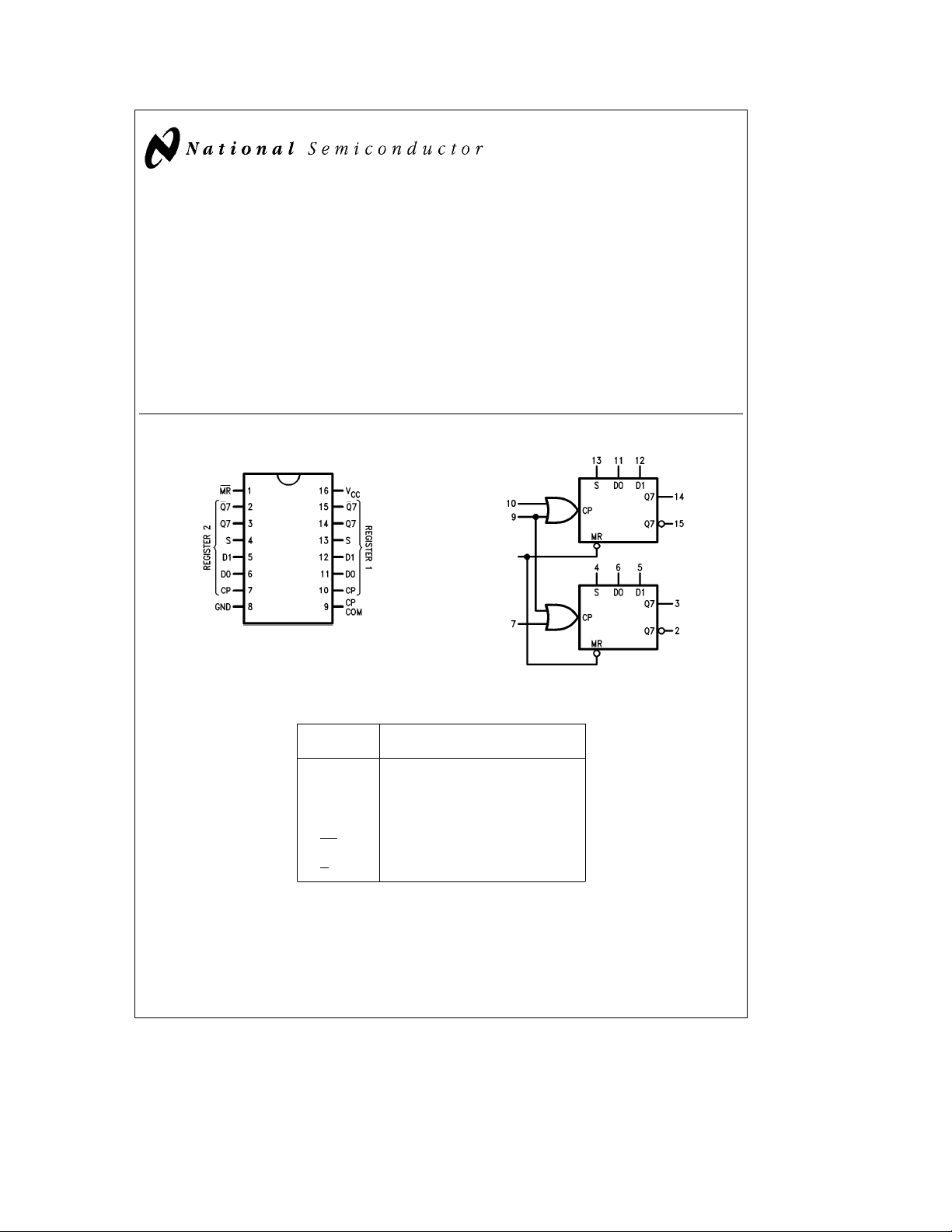
Connection Diagram
Dual-In-Line Package
TL/F/10200– 1
Order Number 93L28DMQB or 93L28FMQB
See NS Package Number J16A or W16A
Features
Y
2-input multiplexer provided at data input of each
register
Y
Gated clock input circuitry
Y
Both true and complementary outputs provided from
last bit of each register
Y
Asynchronous master reset common to both registers
Logic Symbol
V
CC
GND
e
e
Pin 16
Pin 8
TL/F/10200– 2
Pin
Names
S Data Select Input
D0, D1 Data Inputs
CP Clock Pulse Input (Active HIGH)
MR Master Reset Input (Active LOW)
Q7 Last Stage Output
Q
7 Complementary Output
C
1995 National Semiconductor Corporation RRD-B30M105/Printed in U. S. A.
TL/F/10200
Description
Common (Pin 9)
Separate (Pins 7 and 10)

Absolute Maximum Ratings (Note)
Note:
If Military/Aerospace specified devices are required,
please contact the National Semiconductor Sales
Office/Distributors for availability and specifications.
Supply Voltage 7V
Input Voltage 5.5V
Operating Free Air Temperature Range
MIL
Storage Temperature Range
b
55§Ctoa125§C
b
65§Ctoa150§C
The ‘‘Absolute Maximum Ratings’’ are those values
beyond which the safety of the device cannot be guaranteed. The device should not be operated at these limits. The
parametric values defined in the ‘‘Electrical Characteristics’’
table are not guaranteed at the absolute maximum ratings.
The ‘‘Recommended Operating Conditions’’ table will define
the conditions for actual device operation.
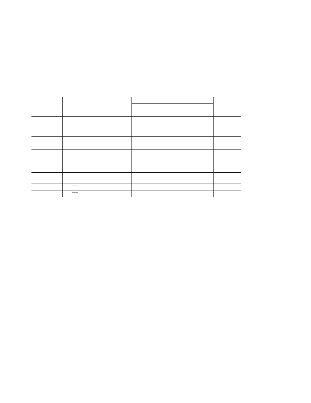
Recommended Operating Conditions
Symbol Parameter
V
CC
V
IH
V
IL
I
OH
I
OL
T
A
ts(H) Setup Time HIGH or LOW 30
t
(L) Dnto CP 30
s
th(H) Hold Time HIGH or LOW 0
th(L) Dnto CP 0
tw(H) Clock Pulse Width 55
t
(L) HIGH or LOW 55
w
tw(L) MR Pulse Width with CP HIGH 60 ns
tw(L) MR Pulse Width with CP LOW 70 ns
Supply Voltage 4.5 5 5.5 V
High Level Input Voltage 2 V
Low Level Input Voltage 0.7 V
High Level Output Current
Low Level Output Current 4.8 mA
Free Air Operating Temperature
Min Nom Max
b
55 125
93L28 (MIL)
b
400 mA
Units
C
§
ns
ns
ns
2
 Loading...