NSC 93L00FMQB, 93L00DMQB Datasheet

93L00
4-Bit Universal Shift Register
93L00 4-Bit Universal Shift Register
June 1989
General Description
The 93L00 is a 4-bit universal shift register. As a high speed
multifunctional sequential logic block, it is useful in a wide
variety of register and counter applications. It may be used
in serial-serial, shift left, shift right, serial-parallel, parallelserial, and parallel-parallel data register transfers.
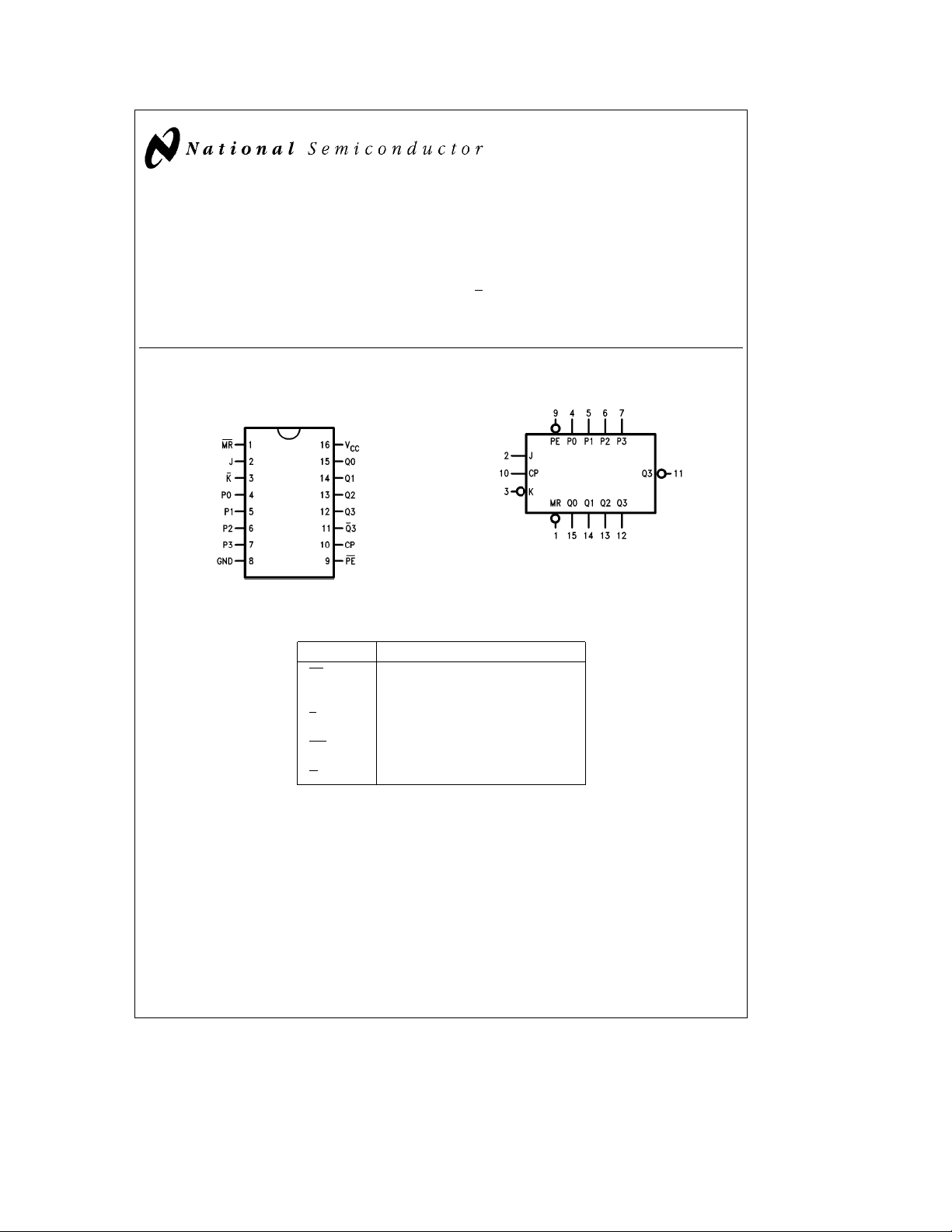
Connection Diagram
Dual-In-Line Package
Order Number 93L00DMQB or 93L00FMQB
See NS Package Number J16A or W16A
Pin Names Description
PE Parallel Enable Input (Active LOW)
P0–P3 Parallel Inputs
J First Stage J Input (Active HIGH)
K
CP Clock Pulse Input (Active Rising Edge)
MR
Q0–Q3 Parallel Outputs
Q
3 Complementary Last Stage Output
TL/F/9576– 1
First Stage K Input (Active LOW)
Master Reset Input
Features
Y
Asynchronous master reset
Y
J, K inputs to first stage
Logic Symbol
V
CC
GND
e
e
Pin 16
Pin 8
TL/F/9576– 2
C
1995 National Semiconductor Corporation RRD-B30M105/Printed in U. S. A.
TL/F/9576

Absolute Maximum Ratings (Note)
Note:
If Military/Aerospace specified devices are required,
please contact the National Semiconductor Sales
Office/Distributors for availability and specifications.
Supply Voltage 7V
Input Voltage 5.5V
Operating Free Air Temperature Range
MIL
b
65§Ctoa125§C
The ‘‘Absolute Maximum Ratings’’ are those values
beyond which the safety of the device cannot be guaranteed. The device should not be operated at these limits. The
parametric values defined in the ‘‘Electrical Characteristics’’
table are not guaranteed at the absolute maximum ratings.
The ‘‘Recommended Operating Conditions’’ table will define
the conditions for actual device operation.
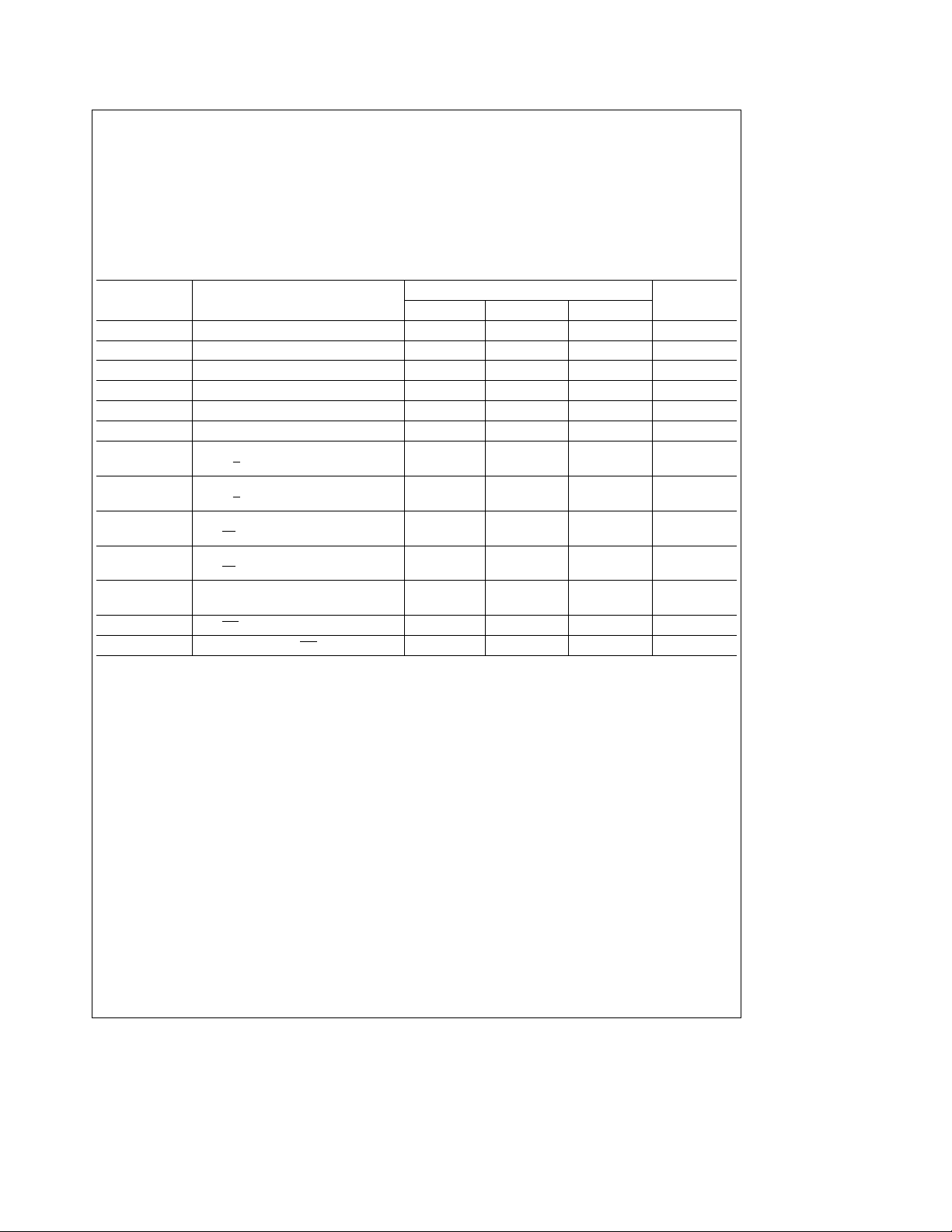
Recommended Operating Conditions
Symbol Parameter
Min Nom Max
V
CC
V
IH
V
IL
I
OH
I
OL
T
A
Supply Voltage 4.5 5 5.5 V
High Level Input Voltage 2 V
Low Level Input Voltage 0.7 V
High Level Output Voltage
Low Level Output Current 4.8 mA
Free Air Operating Temperature
b
55 125
ts(H) Setup Time HIGH or LOW, 60
t
(L) J, K and P0 – P3 to CP 60
s
th(H) Hold Time HIGH or LOW, 0
th(L) J, K and P0 –P3 to CP 0
ts(H) Setup Time HIGH or LOW, 68
t
(L) PE to CP 68
s
th(H) Hold Time HIGH or LOW, 0
t
(L) PE to CP 0
h
tw(H) CP Pulse Width 38
t
(L) HIGH or LOW 38
w
tw(L) MR Pulse Width LOW 53 ns
t
rec
Recovery Time, MR to CP 70 ns
93L00 (MIL)
b
0.4 mA
Units
C
§
ns
ns
ns
ns
ns
2

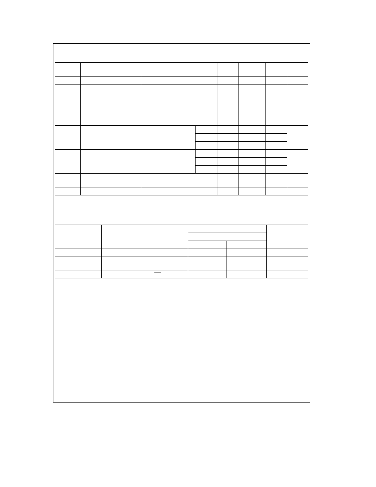
Electrical Characteristics
Over recommended operating free air temperature range (unless otherwise noted)
Symbol Parameter Conditions Min
e
V
I
V
OH
V
OL
I
I
I
IH
I
IL
I
OS
I
CC
Note 1: All typicals are at V
Note 2: Not more than one output should be shorted at a time, and the duration should not exceed one second.
Switching Characteristics
V
CC
Input Clamp Voltage V
High Level Output Voltage V
Low Level Output Voltage V
Input Current@Max V
Input Voltage
High Level Input Current V
Low Level Input Current V
Short Circuit V
Output Current (Note 2)
Supply Current V
e
e
5V, T
CC
A
ea
5.0V, T
ea
25§C (See Section 1 for waveforms and load configurations)
A
25§C.
CC
CC
e
V
IL
CC
e
V
IH
CC
CC
CC
CC
CC
Symbol Parameter C
f
t
t
t
max
PLH
PHL
PHL
Maximum Shift Frequency 10 MHz
Propagation Delay 35
CP to Q
n
Propagation Delay, MR to Q
eb
e
Max, V
e
Min, V
e
e
Min, I
Min, I
Min, I
Max, V
Max, V
10 mA
I
e
Max,
OH
e
Min
IH
e
Max,
OL
e
Max
IL
e
5.5V
I
e
2.4V Inputs 20
I
2.4 3.4 V
CP 40 mA
PE 46
e
Max, V
e
0.3V Inputs
I
CP
PE
e
Max
e
Max 23 mA
b
93L
e
L
Min Max
n
Typ
(Note 1)
Max Units
b
1.5 V
0.3 V
1mA
b
400
b
800 mA
b
920
2.5
b
25 mA
15 pF Units
51
ns
60 ns
3
 Loading...