NSC 5962-8955801LA, 5962-89558013A Datasheet

TL/F/9581
54F/74F651
#
54F/74F652 Transceivers/Registers
December 1994
54F/74F651#54F/74F652
Transceivers/Registers
General Description
These devices consist of bus transceiver circuits with
D-type flip-flops, and control circuitry arranged for multiplexed transmission of data directly from the input bus or
from internal registers. Data on the A or B bus will be
clocked into the registers as the appropriate clock pin goes
to HIGH logic level. Output Enable pins (OEAB, OEBA
) are
provided to control the transceiver function.
Features
Y
Independent registers for A and B buses
Y
Multiplexed real-time and stored data
Y
Choice of non-inverting and inverting data paths
Ð ’F651 inverting
Ð ’F652 non-inverting
Y
Guaranteed 4000V minimum ESD protection
Commercial Military
Package
Package Description
Number
74F651SPC N24C 24-Lead (0.300×Wide) Molded Dual-In-Line
54F651SDM (Note 2) J24F 24-Lead (0.300×Wide) Ceramic Dual-In-Line
74F651SC (Note 1) M24B 24-Lead (0.300×Wide) Molded Small Outline, JEDEC
54F651FM (Note 2) W24C 24-Lead Cerpack
54F651LM (Note 2) E28A 24-Lead Ceramic Leadless Chip Carrier, Type C
74F652SPC N24C 24-Lead (0.300×Wide) Molded Dual-In-Line
54F652SDM (Note 2) J24F 24-Lead (0.300×Wide) Ceramic Dual-In-Line
74F652SC (Note 1) M24B 24-Lead (0.300×Wide) Molded Small Outline, JEDEC
54F652FM (Note 2) W24C 24-Lead Cerpack
54F652LM (Note 2) E28A 24-Lead Ceramic Leadless Chip Carrier, Type C
Note 1:Devices also available in 13×reel. Use suffixeSCX
Note 2:Military grade device with environmental and burn-in processing. Use suffix
e
DMQB, FMQB and LMQB
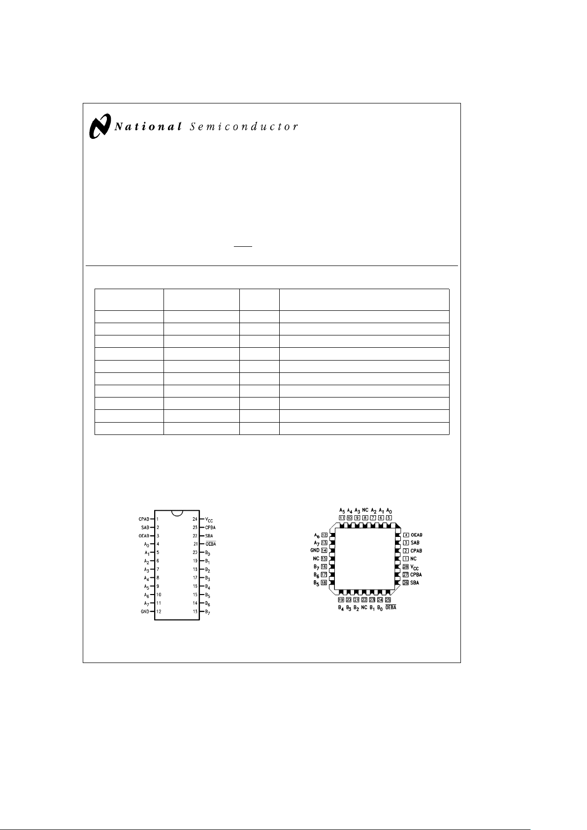
Connection Diagrams
Pin Assignment
DIP, SOIC and Flatpak
TL/F/9581– 3
Pin Assignment
for LCC
TL/F/9581– 4
TRI-STATEÉis a registered trademark of National Semiconductor Corporation.
C
1995 National Semiconductor Corporation RRD-B30M75/Printed in U. S. A.

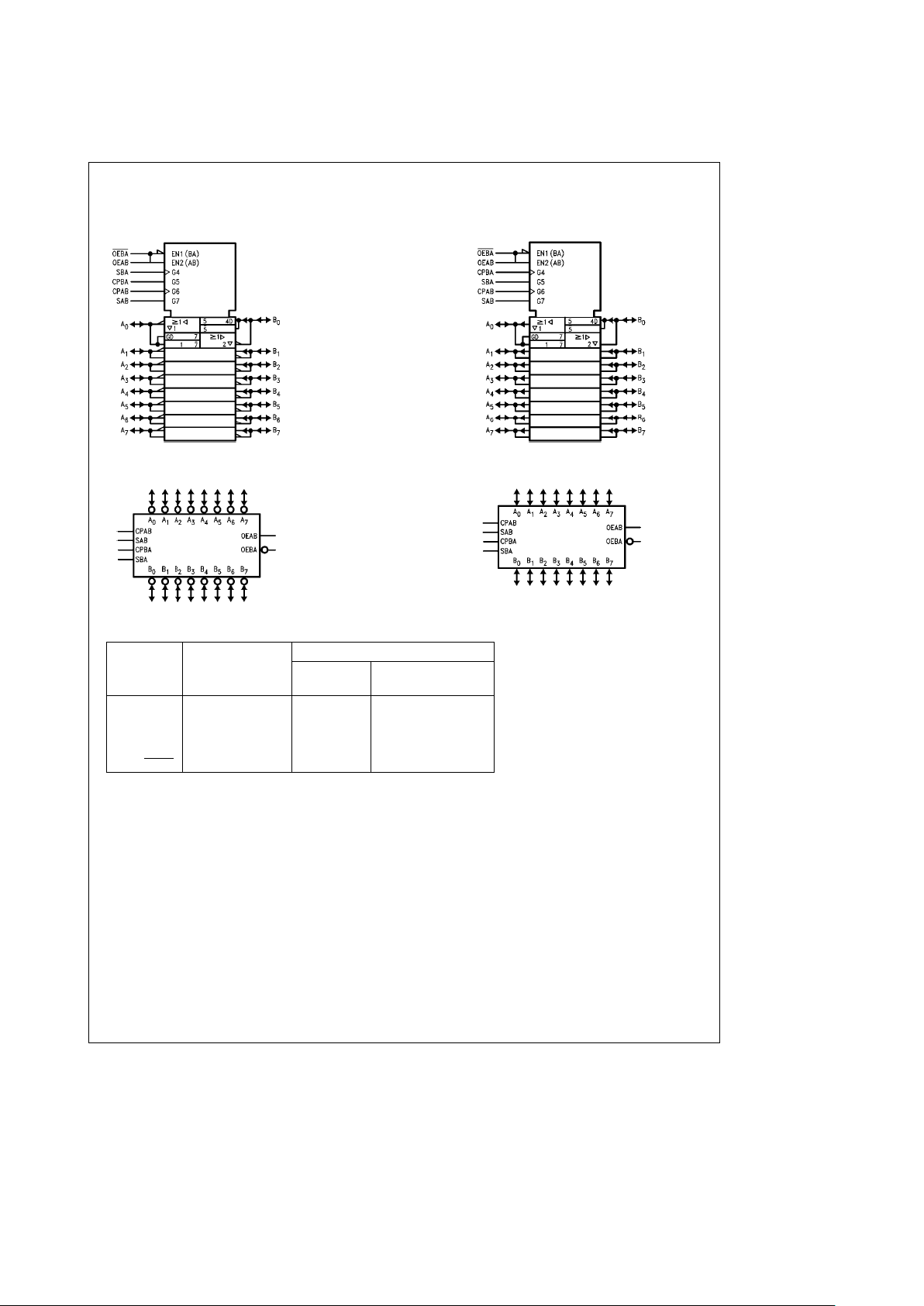
Logic Symbols
IEEE/IEC
’F651
TL/F/9581– 1
’F651
TL/F/9581– 2
IEEE/IEC
’F652
TL/F/9581– 10
’F652
TL/F/9581– 11
Unit Loading/Fan Out
54F/74F
Pin Names Description
U.L. Input I
IH/IIL
HIGH/LOW Output IOH/I
OL
A0–A7,B0–B7A and B Inputs/ 1.0/1.0 20 mA/b0.6 mA
TRI-STATE
É
Outputs 600/106.6 (80)b12 mA/64 mA (48 mA)
CPAB, CPBA Clock Inputs 1.0/1.0 20 mA/
b
0.6 mA
SAB, SBA Select Inputs 1.0/1.0 20 m A/b0.6 mA
OEAB, OEBA
Output Enable Inputs 1.0/1.0 20 mA/b0.6 mA
2

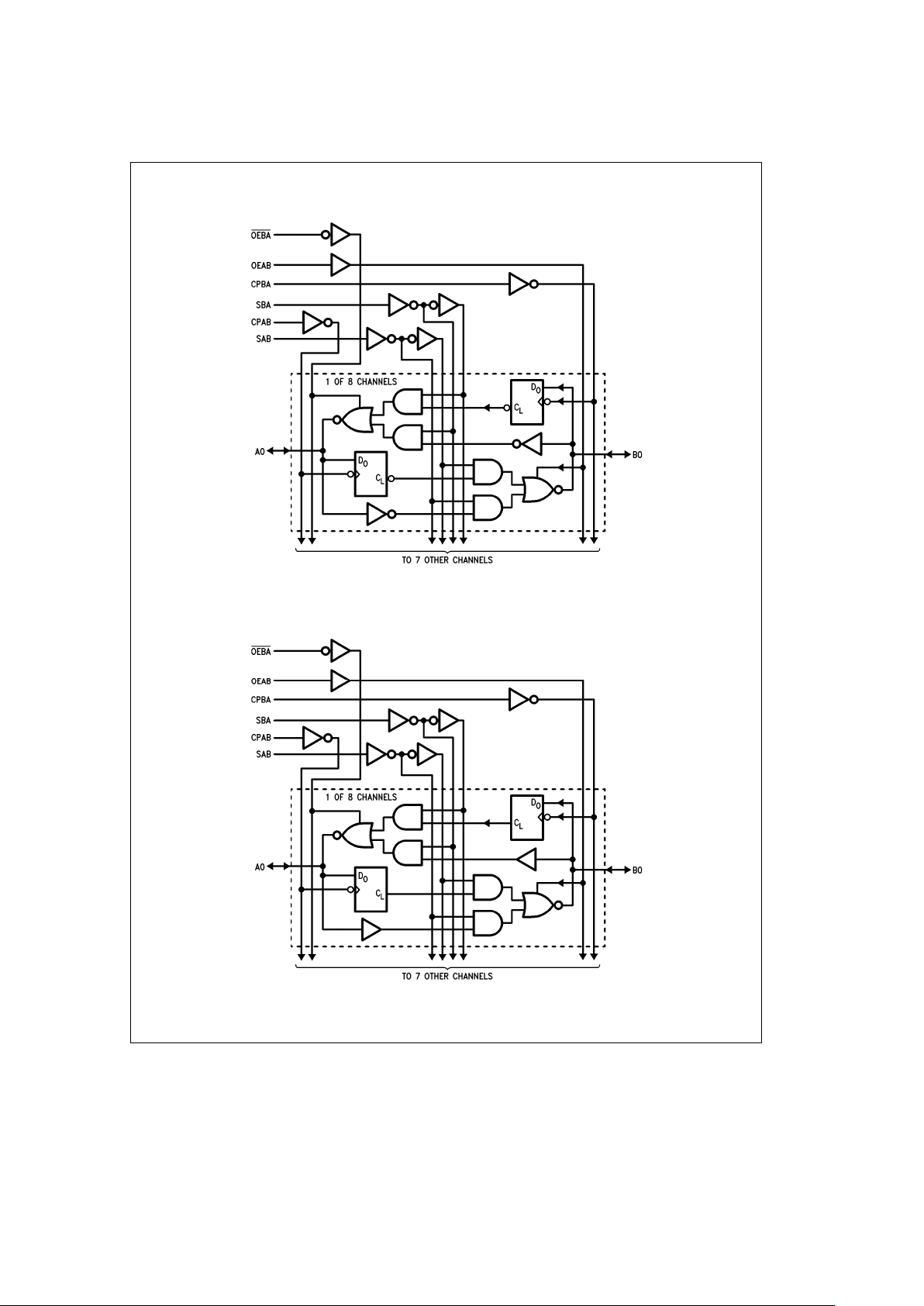
Logic Diagrams
’F652
TL/F/9581– 5
Please note that this diagram is provided only for the understanding of logic operations and should not be used to estimate propagation delays.
’F651
TL/F/9581– 12
Please note that this diagram is provided only for the understanding of logic operations and should not be used to estimate propagation delays.
3
 Loading...