NSC 54F825SDMQB, 54F825LMQB Datasheet

TL/F/9597
54F/74F825 8-Bit D-Type Flip-Flop
December 1994
54F/74F825
8-Bit D-Type Flip-Flop
General Description
The ’F825 is an 8-bit buffered register. It has Clock Enable
and Clear features which are ideal for parity bus interfacing
in high performance microprogramming systems. Also included in the ’F825 are multiple enables that allow multiuser control of the interface.
The ’F825 is functionally and pin compatible with AMD’s
Am29825.
Features
Y
TRI-STATEÉoutput
Y
Clock enable and clear
Y
Multiple output enables
Y
Direct replacement for AMD’s Am24825
Commercial Military
Package
Package Description
Number
74F825SPC N24C 24-Lead (0.300×Wide) Molded Dual-In-Line
54F825SDM (Note 2) J24F 24-Lead (0.300×Wide) Ceramic Dual-In-Line
74F825SC (Note 1) M24B 24-Lead (0.300×Wide) Molded Small Outline, JEDEC
54F825FM (Note 2) W24C 24-Lead Cerpack
54F825LM (Note 2) E28A 24-Lead Ceramic Leadless Chip Carrier, Type C
Note 1: Devices also available in 13×reel. Use suffixeSCX.
Note 2: Military grade device with environmental and burn-in processing. Use suffix
e
SDMQB, FMQB and LMQB.
Logic Symbols
TL/F/9597– 1
IEEE/IEC
TL/F/9597– 4
TRI-STATEÉis a registered trademark of National Semiconductor Corporation.
C
1995 National Semiconductor Corporation RRD-B30M75/Printed in U. S. A.

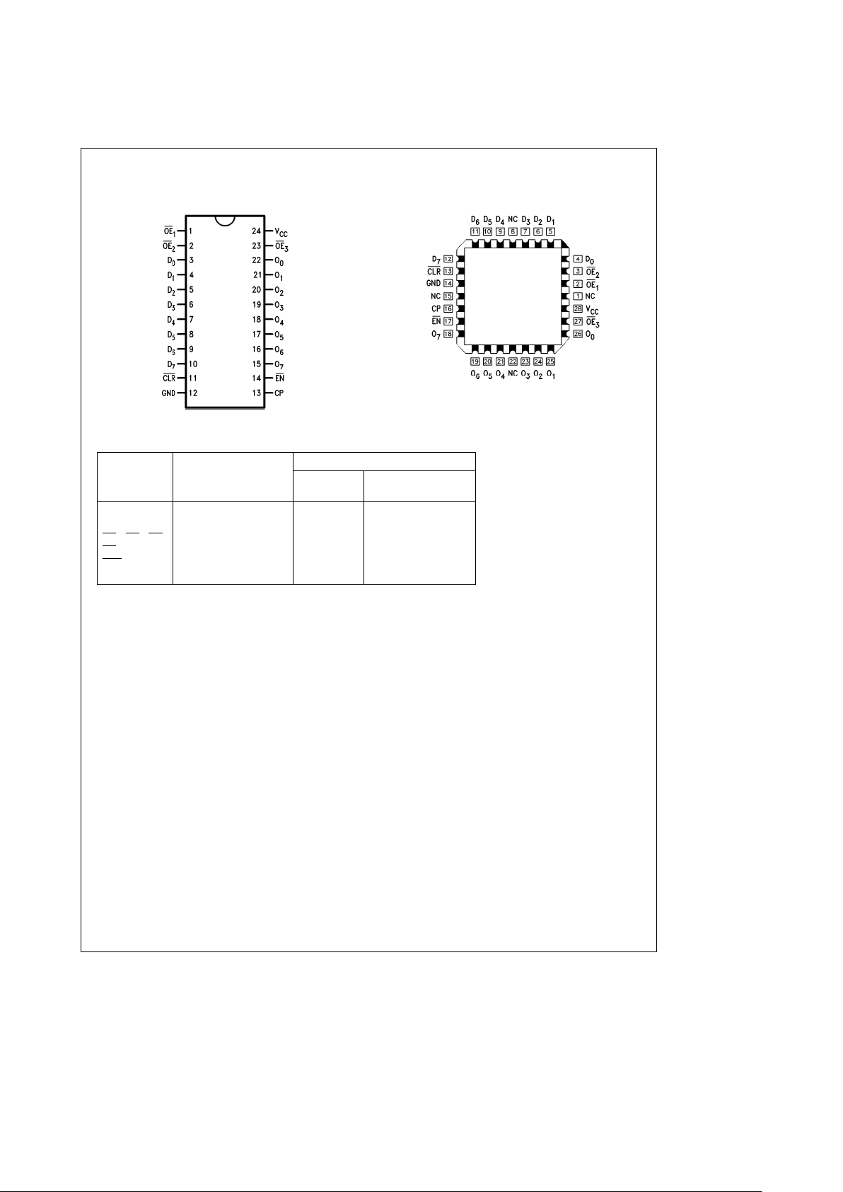
Connection Diagrams
Pin Assignment
for DIP, SOIC and Flatpak
TL/F/9597– 2
Pin Assignment
for LCC
TL/F/9597– 3
Unit Loading/Fan Out
54F/74F
Pin Names Description
U.L. Input I
IH/IIL
HIGH/LOW Output IOH/I
OL
D0–D
7
Data Inputs 1.0/1.0 20 mA/b0.6 mA
O
0–O7
TRI-STATE Data Outputs 150/40 (33.3)b3 mA/24 mA (20 mA)
OE
1
,OE2,OE3Output Enable Input 1.0/1.0 20 mA/b0.6 mA
EN Clock Enable 1.0/1.0 20 mA/b0.6 mA
CLR
Clear 1.0/1.0 20 mA/b0.6 mA
CP Clock Input 1.0/2.0 20 mA/b1.2 mA
2

Functional Description
The ’F825 consists of eight D-type edge-triggered flip-flops.
This device has TRI-STATE true outputs and is organized in
broadside pinning. In addition to the clock and output enable pins, the buffered clock (CP) and buffered Output Enable (OE
) are common to all flip-flops. The flip-flops will
store the state of their individual D inputs that meet the
setup and hold times requirements on the LOW-to-HIGH CP
transition. With the OE
LOW the contents of the flip-flops
are available at the outputs. When the OE
is HIGH, the out-
puts go to the high impedance state. Operation of the OE
input does not affect the state of the flip-flops. The ’F825
has Clear (CLR
) and Clock Enable (EN) pins.
When the CLR is LOW and the OE is LOW the outputs are
LOW. When CLR
is HIGH, data can be entered into the flip-
flops. When EN
is LOW, data on the inputs is transferred to
the outputs on the LOW-to-HIGH clock transition. When the
EN
is HIGH the outputs do not change state, regardless of
the data or clock input transitions.
Function Table
Inputs Internal Output
Function
OE CLR EN CP D Q O
H H L H X NC Z Hold
H H L L X NC Z Hold
H H H X X NC Z Hold
L H H X X NC NC Hold
H L X X X H Z Clear
L L X X X H L Clear
HHLLL H Z Load
HHLLH L Z Load
LHLLL H L Data Available
LHLLH L H Data Available
L H L H X NC NC No Change in Data
L H L L X NC NC No Change in Data
LeLOW Voltage Level
H
e
HIGH Voltage Level
X
e
Immaterial
Z
e
High Impedance
L
e
LOW-to-HIGH Transition
NC
e
No Change
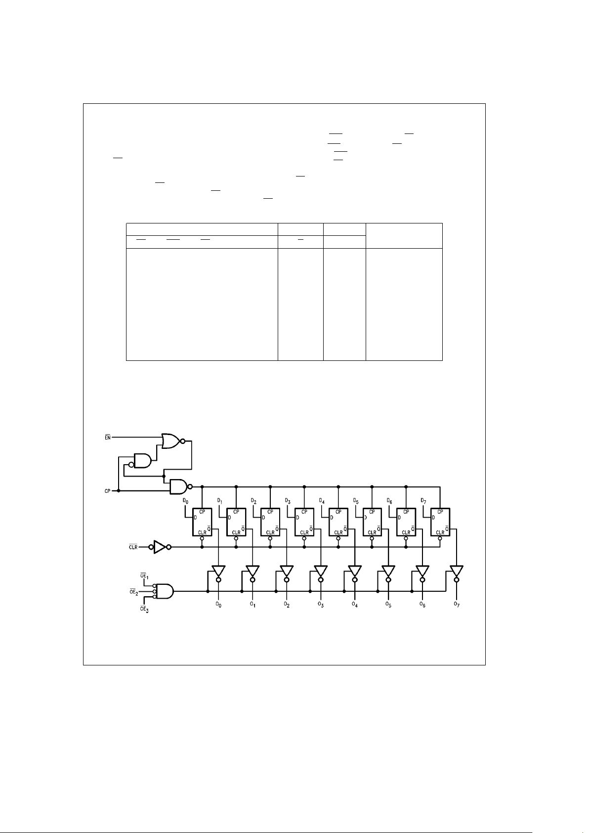
Logic Diagram
TL/F/9597– 5
Please note that this diagram is provided only for the understanding of logic operations and should not be used to estimate propagation delays.
3
 Loading...