

NSC 54F193LMQB, 54F193DMQB, 54F193DC Datasheet

TL/F/9497
54F/74F193 Up/Down Binary Counter with Separate Up/Down Clocks
November 1994
54F/74F193 Up/Down Binary Counter
with Separate Up/Down Clocks
General Description
The ’F193 is an up/down modulo-16 binary counter. Separate Count Up and Count Down Clocks are used, and in
either counting mode the circuits operate synchronously.
The outputs change state synchronously with the LOW-toHIGH transitions on the clock inputs. Separate Terminal
Count Up and Terminal Count Down outputs are provided
that are used as the clocks for subsequent stages without
extra logic, thus simplifying multi-stage counter designs.
Individual preset inputs allow the circuit to be used as a
programmable counter. Both the Parallel Load (PL
) and the
Master Reset (MR) inputs asynchronously override the
clocks.
Features
Y
Guaranteed 4000V minimum ESD protection
Commercial Military
Package
Package Description
Number
74F193PC N16E 16-Lead (0.300×Wide) Molded Dual-In-Line
54F193DM (Note 2) J16A 16-Lead Ceramic Dual-In-Line
74F193SC (Note 1) M16A 16-Lead (0.150×Wide) Molded Small Outline, JEDEC
74F193SJ (Note 1) M16D 16-Lead (0.300×Wide) Molded Small Outline, EIAJ
54F193FM (Note 2) W16A 16-Lead Cerpack
54F193LM (Note 2) E20A 20-Lead Ceramic Leadless Chip Carrier, Type C
Note 1: Devices also available in 13×reel. Use suffixeSCX and SJX.
Note 2: Military grade device with environmental and burn-in processing. Use suffix
e
DMQB, FMQB and LMQB.
Logic Symbols Connection Diagrams
TL/F/9497– 1
IEEE/IEC
TL/F/9497– 4
Pin Assignment
for DIP, SOIC and Flatpak
TL/F/9497– 2
Pin Assignment
for LCC
TL/F/9497– 3
TRI-STATEÉis a registered trademark of National Semiconductor Corporation.
C
1995 National Semiconductor Corporation RRD-B30M75/Printed in U. S. A.
Unit Loading/Fan Out
54F/74F
Pin Names Description
U.L. Input I
IH/IIL
HIGH/LOW Output IOH/I
OL
CP
U
Count Up Clock Input (Active Rising Edge) 1.0/3.0 20 mA/b1.8 mA
CP
D
Count Down Clock Input (Active Rising Edge) 1.0/3.0 20 mA/b1.8 mA
MR Asynchronous Master Reset Input (Active HIGH) 1.0/1.0 20 mA/
b
0.6 mA
PL Asynchronous Parallel Load Input (Active LOW) 1.0/1.0 20 mA/b0.6 mA
P
0–P3
Parallel Data Inputs 1.0/1.0 20 mA/b0.6 mA
Q0–Q3Flip-Flop Outputs 50/33.3b1 mA/20 mA
TC
D
Terminal Count Down (Borrow) Output (Active LOW) 50/33.3b1 mA/20 mA
TC
U
Terminal Count Up (Carry) Output (Active LOW) 50/33.3b1 mA/20 mA
Functional Description
The ’F193 is a 4-bit binary synchronous up/down (reversible) counter. It contains four edge-triggered flip-flops, with
internal gating and steering logic to provide master reset,
individual preset, count up and count down operations.
A LOW-to-HIGH transition on the CP input to each flip-flop
causes the output to change state. Synchronous switching,
as opposed to ripple counting, is achieved by driving the
steering gates of all stages from a common Count Up line
and a common Count Down line, thereby causing all state
changes to be initiated simultaneously. A LOW-to-HIGH
transition on the Count Up input will advance the count by
one; a similar transition on the Count Down input will decrease the count by one. While counting with one clock input, the other should be held HIGH, as indicated in the
Function Table.
The Terminal Count Up (TC
U
) and Terminal Count Down
(TC
D
) outputs are normally HIGH. When the circuit has
reached the maximum count state 15, the next HIGH-toLOW transition of the Count Up Clock will cause TC
U
to go
LOW. TC
U
will stay LOW until CPUgoes HIGH again, thus
effectively repeating the Count Up Clock, but delayed by
two gate delays. Similarly, the TC
D
output will go LOW when
the circuit is in the zero state and the Count Down Clock
goes LOW. Since the TC
outputs repeat the clock waveforms, they can be used as the clock input signals to the
next higher order circuit in a multistage counter.
TC
U
e
Q
0
#
Q
1
#
Q
2
#
Q
3
#
CP
U
TC
D
e
Q
0
#
Q
1
#
Q
2
#
Q
3
#
CP
D
The ’F193 has an asynchronous parallel load capability permitting the counter to be preset. When the Parallel Load
(PL
) and the Master Reset (MR) inputs are LOW, informa-
tion present on the Parallel Data input (P
0–P3
) is loaded
into the counter and appears on the outputs regardless of
the conditions of the clock inputs. A HIGH signal on the
Master Reset input will disable the preset gates, override
both clock inputs, and latch each Q output in the LOW state.
If one of the clock inputs is LOW during and after a reset or
load operation, the next LOW-to-HIGH transition of that
clock will be interpreted as a legitimate signal and will be
counted.
Function Table
MR PL CP
U
CP
D
Mode
H X X X Reset (Asyn.)
L L X X Preset (Asyn.)
L H H H No Change
LHLH Count Up
LH HLCount Down
HeHIGH Voltage Level
L
e
LOW Voltage Level
X
e
Immaterial
L
e
LOW-to-HIGH Clock Transition
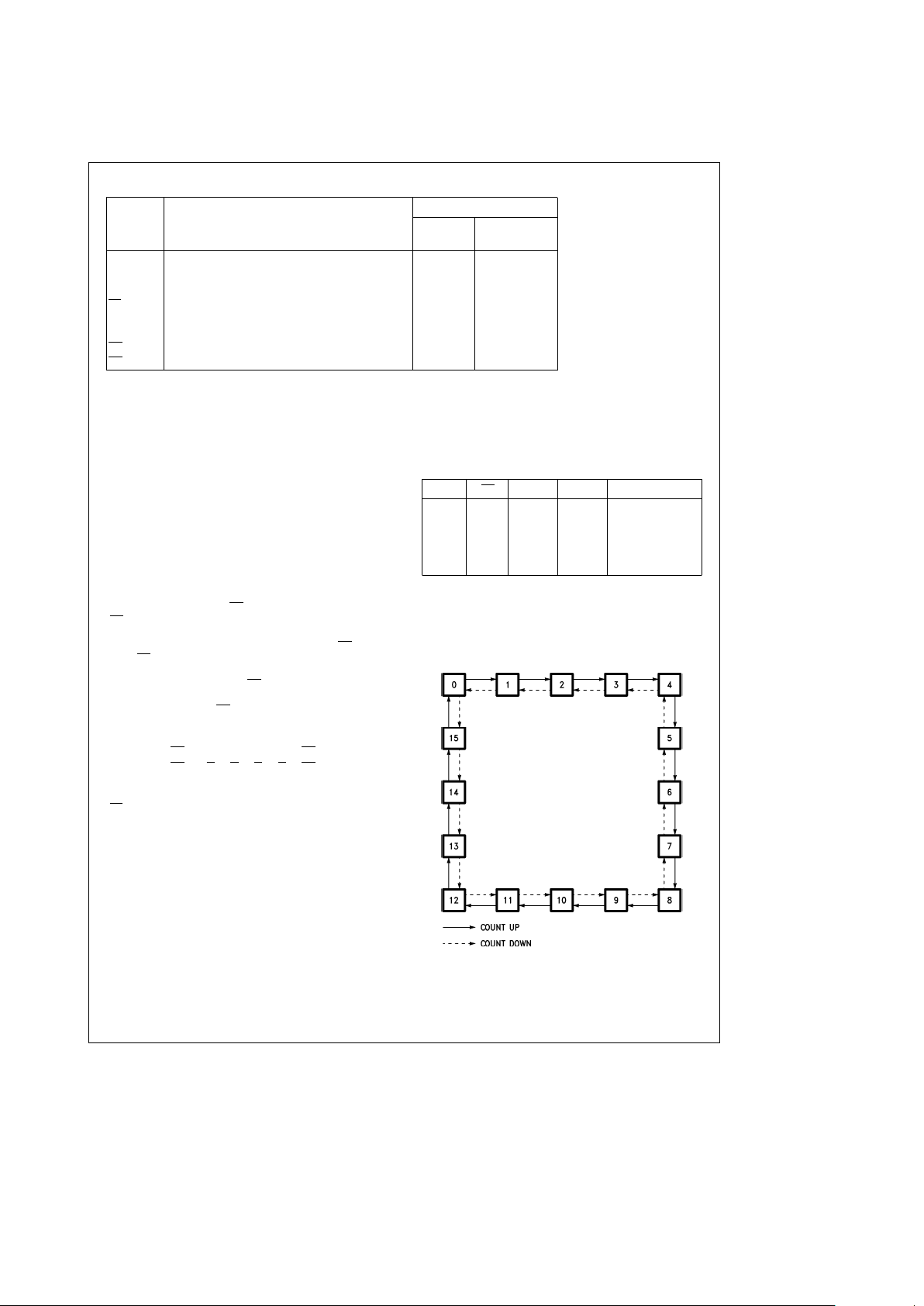
State Diagram
TL/F/9497– 5
2

Logic Diagram
TL/F/9497– 6
Please note that this diagram is provided only for the understanding of logic operations and should not be used to estimate propagation delays.
3
 Loading...