NSC 54F190DMQB Datasheet

TL/F/9494
54F/74F190 Up/Down Decade Counter with Preset and Ripple Clock
November 1994
54F/74F190
Up/Down Decade Counter with Preset and Ripple Clock
General Description
The ’F190 is a reversible BCD (8421) decade counter featuring synchronous counting and asynchronous presetting.
The preset feature allows the ’F190 to be used in programmable dividers. The Count Enable input, the Terminal Count
output and the Ripple Clock output make possible a variety
of methods of implementing multistage counters. In the
counting modes, state changes are initiated by the rising
edge of the clock.
Features
Y
High-speedÐ125 MHz typical count frequency
Y
Synchronous counting
Y
Asynchronous parallel load
Y
Cascadable
Commercial Military
Package
Package Description
Number
74F190PC N16E 16-Lead (0.300×Wide) Molded Dual-In-Line
54F190DM (Note 2) J16A 16-Lead Ceramic Dual-In-Line
74F190SC (Note 1) M16A 16-Lead (0.150×Wide) Molded Small Outline, JEDEC
54F190FM (Note 2) W16A 16-Lead Cerpack
54F190LM (Note 2) E20A 20-Lead Ceramic Leadless Chip Carrier, Type C
Note 1: Devices also available in 13×reel. Use suffixeSCX.
Note 2: Military grade device with environmental and burn-in processing. Use suffix
e
DMQB, FMQB and LMQB.
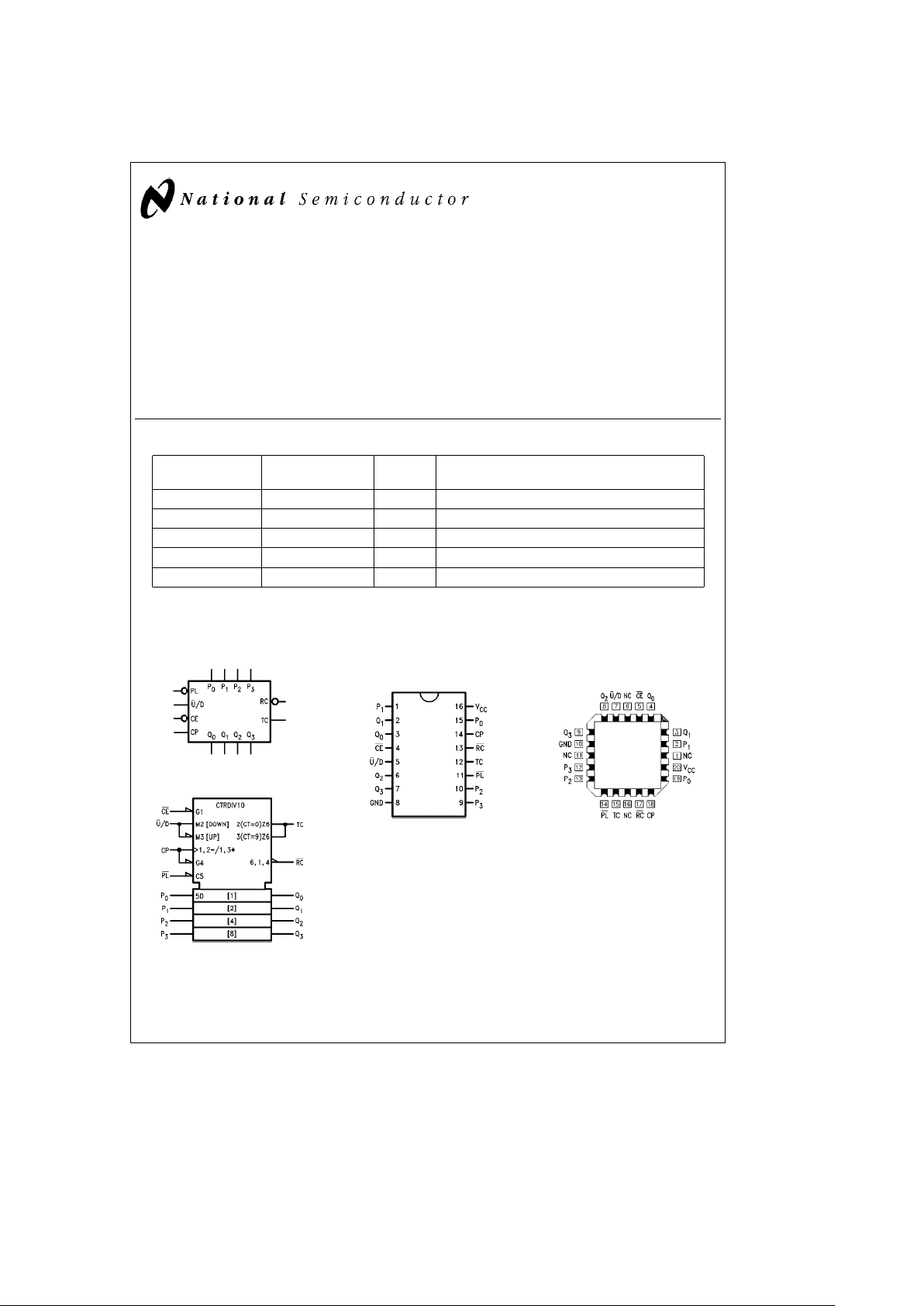
Logic Symbols Connection Diagrams
TL/F/9494– 1
IEEE/IEC
TL/F/9494– 4
Pin Assignment for
DIP, SOIC and Flatpak
TL/F/9494– 2
Pin Assignment
for LCC
TL/F/9494– 3
TRI-STATEÉis a registered trademark of National Semiconductor Corporation.
C
1995 National Semiconductor Corporation RRD-B30M75/Printed in U. S. A.

Unit Loading/Fan Out
54F/74F
Pin Names Description
U.L. Input I
IH/IIL
HIGH/LOW Output IOH/I
OL
CE Count Enable Input (Active LOW) 1.0/3.0 20 mA/b1.8 mA
CP Clock Pulse Input (Active Rising Edge) 1.0/1.0 20 mA/
b
0.6 mA
P
0–P3
Parallel Data Inputs 1.0/1.0 20 mA/b0.6 mA
PL Asynchronous Parallel Load Input (Active LOW) 1.0/1.0 20 mA/b0.6 mA
U
/D Up/Down Count Control Input 1.0/1.0 20 mA/b0.6 mA
Q0–Q
3
Flip-Flop Outputs 50/33.3
b
1 mA/20 mA
RC
Ripple Clock Output (Active LOW) 50/33.3
b
1 mA/20 mA
TC Terminal Count Output (Active HIGH) 50/33.3
b
1 mA/20 mA
Functional Description
The ’F190 is a synchronous up/down BCD decade counter
containing four edge-triggered flip-flops, with internal gating
and steering logic to provide individual preset, count-up and
count-down operations. It has an asynchronous parallel
load capability permitting the counter to be preset to any
desired number. When the Parallel Load (PL
) input is LOW,
information present on the Parallel Data inputs (P
0–P3
)is
loaded into the counter and appears on the Q outputs. This
operation overrides the counting functions, as indicated in
the Mode Select Table. A HIGH signal on the CE
input inhib-
its counting. When CE
is LOW, internal state changes are
initiated synchronously by the LOW-to-HIGH transition of
the clock input. The direction of counting is determined by
the U
/D input signal, as indicated in the Mode Select Table,
CE
and U/D can be changed with the clock in either state,
provided only that the recommended setup and hold times
are observed.
Two types of outputs are provided as overflow/underflow
indicators. The Terminal Count (TC) output is normally LOW
and goes HIGH when a circuit reaches zero in the countdown mode or reaches 9 in the count-up mode. The TC
output will then remain HIGH until a state change occurs,
whether by counting or presetting or until U
/D is changed.
The TC output should not be used as a clock signal because it is subject to decoding spikes. The TC signal is also
used internally to enable the Ripple Clock (RC
) output. The
RC
output is normally HIGH. When CE is LOW and TC is
HIGH, the RC
output will go LOW when the clock next goes
LOW and will stay LOW until the clock goes HIGH again.
This feature simplifies the design of multistage counters.
For a discussion and illustrations of the various methods of
implementing multistage counters, please see the ’F191
data sheet.
RC
Truth Table
Inputs Output
CE TC* CP RC
LHßß
HX X H
XL X H
*TC is generated internally
H
e
HIGH Voltage Level
L
e
LOW Voltage Level
X
e
Immaterial
L
e
LOW-to-HIGH Clock Transition
ß
e
LOW Pulse
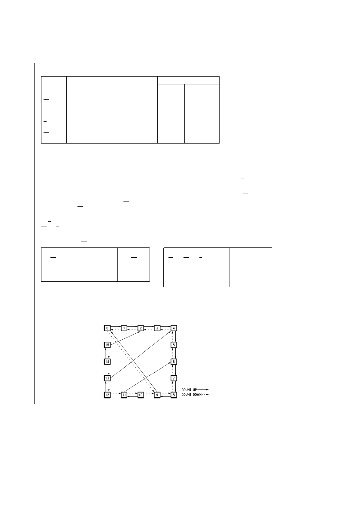
Mode Select Table
Inputs
Mode
PL CE U/D CP
HL LLCount Up
HL HLCount Down
L X X X Preset (Asyn.)
H H X X No Change (Hold)
State Diagram
TL/F/9494– 5
2

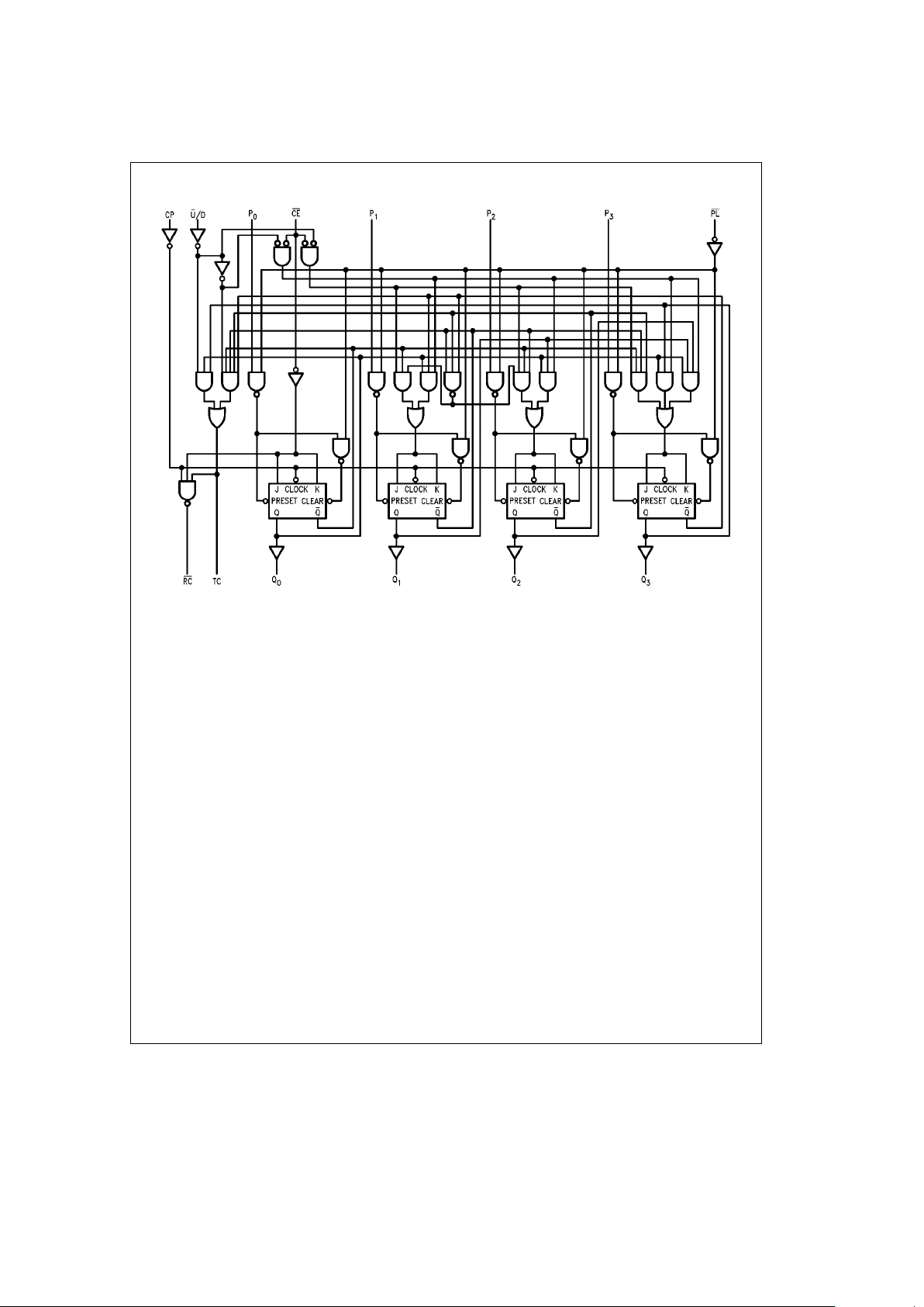
Logic Diagram
TL/F/9494– 6
Please note that this diagram is provided only for the understanding of logic operations and should not be used to estimate propagation delays.
3
 Loading...