

−
CF5746 Series
NIPPON PRECISION CIRCUITS INC.
OVERVIEW
The CF5746 Series devices are analog clock ICs that
derive their timing from a 32 kHz oscillator element.
They feature alarm outputs, snooze function and
alarm auto-stop function. They can be configured to
match a wide variety of clock specifications, alarm
functions and motor outputs.
FEATURES
■
32.768 kHz oscillator circuit
•R
and R
f
built-in
d
• Oscillator capacitance built-in
-C
= 30 pF (typ, excluding CF5746ADC)
D
-C
= 20 pF (typ, CF5746ADC)
D
SERIES CONFIGURATION
CMOS Analog Clock IC
■
Alarm outputs
• Compatible with electronic sound alarms and
motor bells
• 4-step increasing volume alarm output
(CF5746AAB, ADC, AEA, AFA (AO1), AGA
(AO1))
■
Snooze function
• Temporarily stops alarm output and then restarts after a fixed time
■
Debouce circuit (AI/SNZ pin)
■
Test functions
• Shortening snooze time and auto-stop time
• Increasing motor speed (excluding
CF5746BCA)
Power-ON clear function
■
1.5 V supply voltage
■
Chip form
■
CF5746AAB CF5746ABA CF5746BCA CF5746ADC CF5746AEA CF5746AFA CF5746AGA
XT pin C
Built-in
capacitance
Motor output
AI/SNZ input
Alarm output
Pad layout AABAAAA
Other Power-ON clear, oscillator R
1. A
O has the opposite polarity to AO only when output (same phase when non-active).
2. AS = auto-stop
(pF) None None None None None None None
G
pin C
XT
(pF) 30 30 30 20 30 30 30
G
Active level HIGH HIGH – HIGH HIGH HIGH HIGH
Needle period t
Pulsewidth t
Alarm active level LOW LOW LOW HIGH LOW LOW LOW
Pin type 512 Hz 512 Hz 512 Hz 512 Hz 512 Hz Pull-up Pull-up
SNZ interface Yes Yes Yes No Yes Yes Yes
SNZ time t
Bounce delay (ms) 31.25 31.25 31.25 31.25 31.25 31.25 31.25
SNZ release No No No No No Yes (2 s) Ye s (2 s)
Pins AO A
Active level HIGH LOW
Frequency f
Modulation f
Duty (%)
Step time
(s)
min (mA)
I
OH
I
min (mA) 0.8 0.8 0.8 0.8 0.8 0.8 0.002 0.002 0.8 0.8 0.002 0.8 0.002 0.8
OL
Auto-stop t
CY
(s) 1 1 0.125 1111
PW
(ms) 23.4375 31.25 50% duty 46.875 31.25 46.875 31.25
(s) 256 256 256 256 256 256 256
SNZ
O AO1 AO2 AO1 AO2 AO AO AO AO AO1 AO2 AO1 AO2
1
PW
(Hz) 4096 4096 DC DC D C DC 2048 2048 2048 2048 2048 DC 2048 DC
(Hz) 8+1 8+1 ––––8+18+18+18+18+1–8+1–
CY
Step 1 12.5 12.5 ––––6.26 6.26 6.26 6.26 12.5 – 6.26 –
Step 2 25 25 ––––12.5 12.5 12.5 12.5 25 – 12.5 –
Step 3 50 50 ––––2525505050–50–
Step 4 ––––––5050––––––
Step 1 0 to 7 0 to 7 ––––0 to 30 to 30 to 70 to 70 to 7–0 to 7–
Step 2 7 to 15 7 to 15 ––––3 to 73 to 77 to 157 to 157 to 15–7 to 15–
Step 3
Step 4 ––––––
STOP
15 to
2
AS
0.8 − 0.8 − 0.8 − 0.8 − 0.8 − 0.8 − 0.8 − 0.8 − 0.8 − 0.8 − 0.8 − 0.8 − 0.8 − 0.8
(s) 128 128 128 128 128 128 128
HIGH HIGH HIGH HIGH HIGH LOW
15 to
––––7 to 317 to 31
AS
31 to AS31 to
1
HIGH LOW
15 to AS15 to AS15 to
––––––
AS
and R
d
f
built-in
1
HIGH HIGH HIGH HIGH
–
AS
15 to
AS
–
NIPPON PRECISION CIRCUITS—1
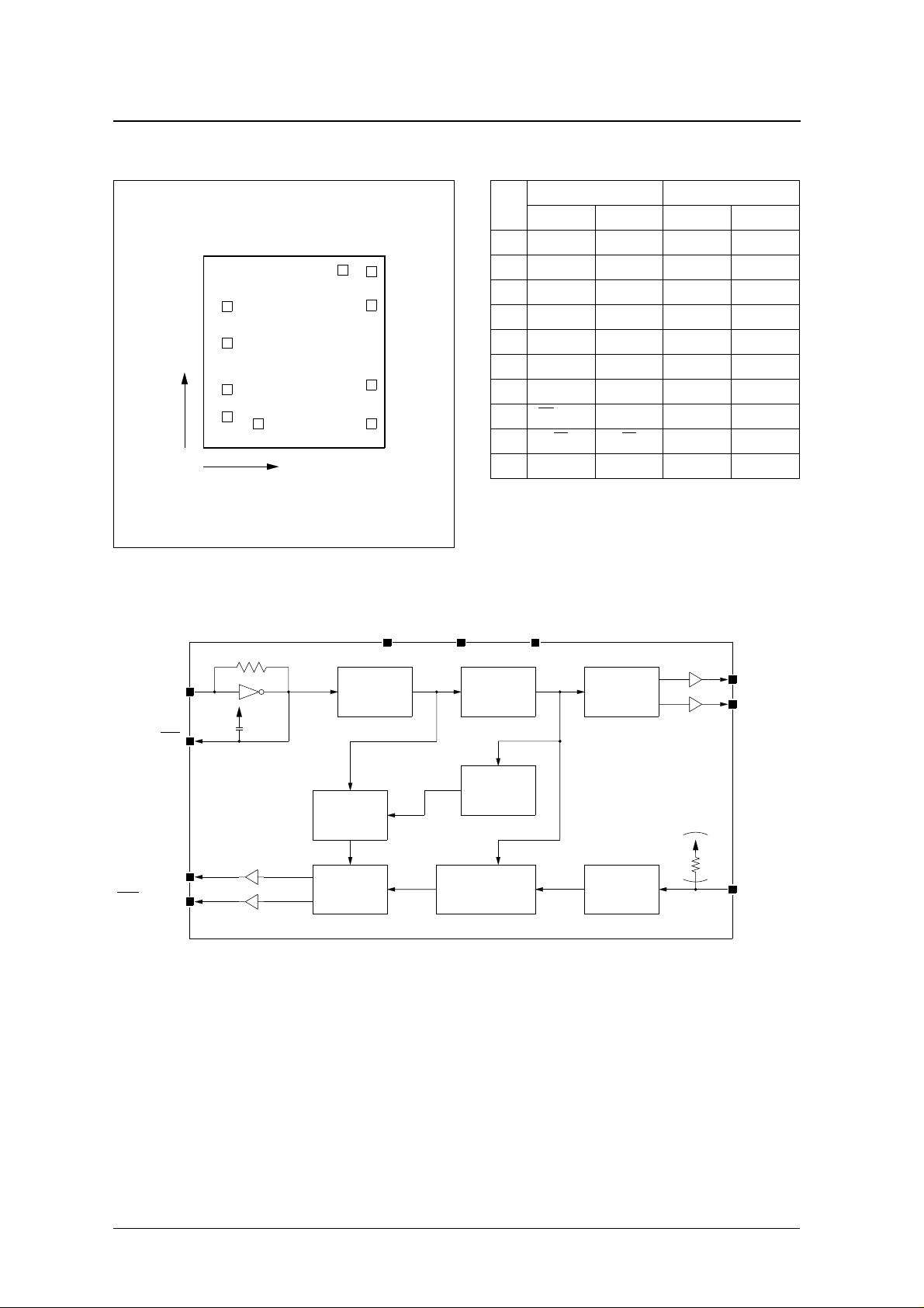
PAD DIMENSIONS
CF5746 Series
1
2
3
Y
4
(0, 0)
5
X
BLOCK DIAGRAM
10
9
8
7
6
TEST VSS
VDD
No.
1 VDD VSS 166 1210
2 VS S VDD 166 882
3 OUT1 AI/SNZ 166 474
4 AI/SNZ AO1 166 228
5 TEST AO2 444 169
6 OUT2 OUT1 1444 169
7 AO (AO1) OUT2 1444 513
8A
9XT XT 1444 1516
10 XT XT 1192 1531
Chip size: 1.61 × 1.70 mm
Chip thickness: 400 ± 30 µm
Pad size: 100 × 100 µm
Chip surface is at V
Layout Dimensions (µm)
A (ex. BCA) B (BCA) X Y
O (AO2) TEST 1444 1219
potential.
DD
XT
XT
AO(AO1)
AO(AO2)
CD
4- Stage
Divider
AO Duty
Control
Alarm
Out
11- Stage
Divider
4- Stage
Divider
Snooze
Counter
Output
Control
Input
Control
OUT1
OUT2
AI/SNZ
NIPPON PRECISION CIRCUITS—2
PIN DESCRIPTION
Name Description
VDD Positive supply voltage pin
VSS Ground pin
XT Oscillator input pin
XT
OUT1 Motor output pin 1
OUT2 Motor output pin 2
AI/SNZ Alarm/snooze input pin
AO (AO1) Alarm output pin
AO (AO2) Alarm output pin
TEST Test pin
Oscillator output pin
−
−
−
°
−
° C
−
−
−
−
− 1 − 3 −
∆
CF5746 Series
SPECIFICATIONS
Absolute Maximum Ratings
Parameter Symbol Condition Rating Unit
Supply voltage range V
Input voltage range V
Operating temperature range T
Storage temperature range T
Electrical Characteristics
T
= 25 ° C, V
a
Operating voltage V
Current consumption
Motor output current I
Alarm HIGH-level output current I
Alarm LOW-level output current
Alarm LOW-level output current
AI/SNZ HIGH-level input voltage V
AI/SNZ LOW-level input voltage V
AI/SNZ HIGH-level output current I
AI/SNZ LOW-level output current I
Oscillator frequency stability
VDD-to-XT pin built-in
capacitance
VDD-to-XT
capacitance
= 1.5 V, V
DD
Parameter Symbol Condition
1
2
3
pin built-in
= 0 V, f
SS
DD
DD
I
DD
MOT
OH
I
OL
IH
IL
OH
OL
f/f V
C
G
C
D
V
SS
IN
opr
stg
= 32.768 kHz unless otherwise noted
0
0.3 to 5.0 V
V
to V
SS
DD
30 to 70
40 to 125
Rating
min typ max
1.2 – 2.0 V
No load
– 1.0 2.0 µA
V
DD
V
DD
V
DD
= 1.2 V, R
= 1.2 V , V
= 1.2 V , V
= 200 Ω
L
= 0.7 V
OH
= 0.5 V 0.8 1.5 – mA
OL
±3.8 – – mA
0.8
1.5 – mA
21530µA
V
0.2 – V
DD
V
SS
V
= V
1.5 V
+ 1.5 V
Excluding
CF5746AFA,
AGA
1310µA
OH
DD
= V
V
OL
DD
= 1.2 to 2.0 V – 0.5 1 ppm/0.1 V
DD
–V
DD
+ 0.2 V
SS
10 µA
– None – pF
Excluding CF5746ADC – 30 – pF
CF5746ADC – 20 – pF
V
C
Unit
V
1. All pins except the supply and crystal oscillator pins are open.
2. CF5746AAB, ABA, BCA, AEA, AFA (AO2), AGA (AO2)
3. CF5746ADC, AFA (AO1), AGA (AO2)
NIPPON PRECISION CIRCUITS—3

CF5746 Series
FUNCTIONAL DESCRIPTION
Alarm Input/Output
AI/SNZ input Deboucing circuit
A bounce delay is provided on the AI/SNZ input,
regardless of whether the input is LOW or HIGH, to
eliminate erroneous operation caused by input
bounce. For t
snooze input signal is ignored. For t
the alarm input or snooze input is accepted.
Alarm/snooze function
31.25 ms, any alarm input or
ON
ON
62.5 ms,
≤
≥
An active level on AI/SNZ for ≥ 62.5 ms triggers the
alarm function, and alarm operation starts.
During alarm output, an active level on AI/SNZ for ≥
62.5 ms triggers the snooze function. In snooze
mode, the alarm output is temporarily stopped for an
interval of approximately 256 seconds. After this
interval ends, alarm output restarts.
For devices other than the CF5746ADC, the snooze
interval count is restarted from 0 if another snooze
input is received while in snooze mode. After the
snooze interval ends, alarm output restarts.
For the CF5746AFA and AGA, an active level on
AI/SNZ for ≥ 2 s in snooze mode cancels the snooze
and immediately the alarm signal restarts (snooze
release).
CF5746AAB CF5746ABA CF5746BCA CF5746ADC CF5746AEA CF5746AFA CF5746AGA
Alarm active level LOW LOW LOW HIGH LOW LOW LOW
SNZ interface Yes Yes Yes No Yes Yes Yes
SNZ
SNZ time t
SNZ release No No No No No Yes (2 s) Yes (2 s)
(s) 256 256 256 256 256 256 256
Alarm output
The CF5746 Series devices feature a combination of
various alarm output options to cover a wide range of
clock specifications.
■
Step output function (CF5746AAB, ADC, AEA,
AFA (AO1), AGA (AO1))
The alarm output increases in volume over 3 or 4
steps, depending on the device selected.
■
Auto-stop function
After the alarm has been active continuously for
128 seconds, auto-stop mode becomes active and
the output stops.
Pins AO A
Active level HIGH LOW
PW
Frequency f
Modulation f
Duty (%)
Step time
(s)
Auto-stop t
1. AO has the opposite polarity to AO only when output (same phase when non-active).
2. AS = auto-stop
CY
Step 1 12.5 12.5 ––––6.26 6.26 6.26 6.26 12.5 – 6.26 –
Step 2 25 25 ––––12.5 12.5 12.5 12.5 25 – 12.5 –
Step 3 50 50 ––––2525505050–50–
Step 4 ––––––5050––––––
Step 1 0 to 7 0 to 7 ––––0 to 30 to 30 to 70 to 70 to 7–0 to 7–
Step 2 7 to 15 7 to 15 ––––3 to 73 to 77 to 157 to 157 to 15–7 to 15–
Step 3
Step 4 ––––––31 to AS31 to AS––––––
STOP
CF5746AAB CF5746ABA CF5746BCA CF5746ADC CF5746AEA CF5746AFA CF5746AGA
O AO1 AO 2 AO1 AO 2 AO AO AO AO AO1 AO2 AO1 AO2
1
HIGH HIGH HIGH HIGH HIGH LOW
(Hz) 4096 4096 DC D C DC DC 2048 2048 2048 2048 2048 DC 2048 D C
(Hz) 8+1 8+1 ––––8+18+18+18+18+1–8+1–
15 to
15 to AS––––7 to 317 to 3115 to AS15 to AS15 to AS–15 to AS–
2
AS
(s) 128 128 128 128 128 128 128
1
HIGH LOW
1
HIGH HIGH HIGH HIGH
NIPPON PRECISION CIRCUITS—4

CF5746 Series
Motor Output
The motor output can be matched to the clock using
a step needle movement (3 options) or a continuous
needle movement (1 option), depending on the
device selected.
CF5746AAB CF5746ABA CF5746BCA CF5746ADC CF5746AEA CF5746AFA CF5746AGA
Active level HIGH HIGH – HIGH HIGH HIGH HIGH
Needle period t
Pulsewidth t
Movement Step Step Continuous Step Step Step Step
CY
(s) 1 1 0.125 1111
(ms) 23.4375 31.25 50% duty 46.875 31.25 46.875 31.25
PW
Test Functions
Open-circuit output
When AI/SNZ is open circuit, a 512 Hz tone is
output (except on the CF5746AFA and AGA).
Time shortening function
This function is used to reduce the alarm output
snooze interval and the auto-stop time. This function
is active under either of the following conditions.
■
TEST must be HIGH.
■
OUT1 and OUT2 must both be HIGH.
Note that devices other than the CF5746BCA (that
is, the step needle movement devices) also have
reduced motor output needle periods for the case
where TEST is HIGH.
TEST = HIGH OUT1 = OUT2 = HIGH
Motor output needle period 1/4 1/4 ––––
Alarm output Unmodulated – – Unmodulated – –
Auto-stop time 1/1024 1/1024 1/1024 1/1024 1/1024 1/1024
Snooze interval 1/1024 1/1024 1/1024 1/1024 1/1024 1/1024
Device
AAB
ADC
AEA
AFA (AO1)
AGA (AO1)
ABA
AFA (AO2)
AGA (AO2)
BCA
AAB
ADC
AEA
AFA (AO1)
AGA (AO1)
ABA
AFA (AO2)
AGA (AO2)
BCA
Power-ON Clear Function
When power is first applied, the snooze state and
alarm auto-stop state are reset to their default values.
NIPPON PRECISION CIRCUITS—5

CF5746 Series
TIMING DIAGRAMS
Motor Output (Step Movement): excluding CF5746BCA
Alarm Output: CF5746AAB, ADC, AEA, AFA (AO1), AGA (AO1)
OUT1
tPW
OUT2
tPW
AO
AO
tCY
1sec
fPW
fCY1
tCY
1sec
fCY2
Motor Output (Continuous Movement): CF5746BCA
OUT1
tCY
125msec
OUT2
tCY
125msec
Alarm Step Output: CF5746AAB, ADC, AEA, AFA (AO1), AGA (AO1)
AO
AO
fPW
NIPPON PRECISION CIRCUITS—6

Alarm/Snooze Input and Alarm Output
CF5746 Series
AI/ SNZ
AO, AO1
AO
*2
AO1 , AO2
(DC Output)
512Hz
*1
tON 62.5
tON 62.5
msec
msec
tON 62.5
msec
tON 62.5
*3
msec
tON 2
sec
tON 62.5
msec
tSNZ
(Restart)
tSNZ= 0
sec
*4
*5
*4
tSTOP= 128
sec
tSNZ
*1: CF5746AFA, AGA
*2: CF5746ABA, BCA
*3: CF5746AAB, ABA, BCA, ADC, AEA
*4: CF5746AFA, AGA
*5: CF5746AAB, ABA, BCA, AEA, AFA, AGA
Alarm/Snooze Input (
AI/ SNZ
(L to H)
AI/ SNZ
(H to L)
NIPPON PRECISION CIRCUITS INC. reserves the right to make changes to the products described in this data sheet in order to
improve the design or performance and to supply the best possible products. Nippon Precision Circuits Inc. assumes no responsibility for
the use of any circuits shown in this data sheet, conveys no license under any patent or other rights, and makes no claim that the circuits
are free from patent infringement. Applications for any devices shown in this data sheet are for illustration only and Nippon Precision
Circuits Inc. makes no claim or warr anty that such applications will be suitab le for the use specified without further testing or modification.
The products described in this data sheet are not intended to use for the apparatus which influence human lives due to the failure or
malfunction of the products. Customers are requested to comply with applicable laws and regulations in effect now and hereinafter,
including compliance with export controls on the distribution or dissemination of the products. Customers shall not expor t, directly or
indirectly, any products without first obtaining required licenses and approvals from appropriate government agencies.
NIPPON PRECISION CIRCUITS INC.
Deboucing
Circuit)
tCH
tON
NIPPON PRECISION CIRCUITS INC.
4-3, 2-chome Fukuzumi
Koutou-ku, Tokyo 135-8430, Japan
Telephone: 03-3642-6661
Facsimile: 03-3642-6698
NC9417AE 1996.04
NIPPON PRECISION CIRCUITS—7
 Loading...