

Page 1
PROFIBUS-DP MANUAL FOR
FD67 MODULES
ISSUE 1
Page 2

FD67 Profibus-DP Manual
Table of contents
1 REGARDING THIS MANUAL...................................................................................1
1.1 Chapter overview........................................................................................................................ 1
2 SAFETY INSTRUCTIONS ........................................................................................2
2.1 Designated use........................................................................................................................... 2
2.2 Qualified personnel.................................................................................................................... 3
2.3 Explanation of symbols.............................................................................................................. 4
2.3.1
Use of attention signs............................................................................................................... 4
2.3.2 Use of danger signs ................................................................................................................. 4
2.3.3 Use of numbering in illustrations...............................................................................................4
2.3.4 Use of handling instructions...................................................................................................... 4
2.3.5 Use of foot notes...................................................................................................................... 4
3 CONFIGURATION INFORMATION.......................................................................... 5
3.1
FD67 in a Profibus-DP network.................................................................................................. 5
3.1.1 System components ................................................................................................................. 5
3.1.1.1 Profibus cables............................................................................................................... 5
3.1.2 General information for successful planning in a Profibus network ............................................ 6
3.1.3 Topology .................................................................................................................................. 6
3.1.4 Termination of bus segments.................................................................................................... 6
3.1.5 Baud rate ................................................................................................................................. 7
3.1.6 Address.................................................................................................................................... 7
3.1.7 Spur lines................................................................................................................................. 7
3.1.8 Design guidelines..................................................................................................................... 7
4 MOUNTING AND WIRING........................................................................................8
4.1 Bus node......................................................................................................................................8
4.2 Assembling the hood of the bus node....................................................................................... 9
4.3 Functional ground....................................................................................................................10
4.4
Power supply ............................................................................................................................ 11
4.5 Profibus connection ................................................................................................................. 12
4.6 Terminal resistors..................................................................................................................... 13
5 SETUP ....................................................................................................................14
5.1 GSD file..................................................................................................................................... 14
5.2 Allocating and setting the Profibus address........................................................................... 15
Page 3

FD67 Profibus-DP Manual
5.3 Configuration.............................................................................................................................16
5.3.1 Placeholder.............................................................................................................................16
5.3.2 Structure of a configuration string............................................................................................17
5.3.3 Replacing DI modules by DIO modules ...................................................................................18
5.3.4 Configuration examples...........................................................................................................19
5.3.4.1 Configuration of compact modules.................................................................................19
5.3.4.2 Configuration with placeholders .....................................................................................20
5.3.4.3 Configuration with expander modules ............................................................................22
5.3.4.4 Configuration with preconfigured modules .....................................................................23
5.3.4.5 Manual assembling of a configuration string ..................................................................24
5.4 Parameterisation.......................................................................................................................25
5.4.1 Parameter message ................................................................................................................26
5.4.1.1 Structure of the standard specific parameters (bytes 0 to 6)...........................................26
5.4.1.2 User parameters............................................................................................................27
5.4.2 Preconfigured modules ...........................................................................................................28
6 SETUP EXAMPLE : STEP BY STEP..................................................................... 29
6.1.1 Mechanical structure ...............................................................................................................29
6.1.1.1 Mounting the hood of the bus node................................................................................29
6.1.1.2 Interconnecting system components ..............................................................................30
6.1.2 Configuration with S7 Hardware Manager ...............................................................................31
7 DIAGNOSIS............................................................................................................ 34
7.1.1 Behaviour in case of interrupted communication......................................................................34
7.2 LED displays..............................................................................................................................35
7.2.1 General information.................................................................................................................35
7.2.2 Bus node ................................................................................................................................35
7.2.2.1 Bus node response to faulty supply voltage ...................................................................37
7.2.3 Displays of digital I/O modules ................................................................................................38
7.2.3.1 LED displays of digital I/O modules................................................................................38
7.2.3.2 Relationship between signal-logical representation and LED response .........................40
7.2.4 Displays of analogue I/O modules ...........................................................................................41
7.2.4.1 Bus IN – LED displays...................................................................................................41
7.2.4.2 M12 sockets – LED Diagnosis displays..........................................................................41
7.2.5 Power distributor displays .......................................................................................................42
7.3 Profibus .....................................................................................................................................43
7.3.1 Diagnosis Overflow .................................................................................................................44
7.3.2 Structure of a diagnosis message............................................................................................45
7.3.2.1 Bytes 0 to 5 : standard diagnostic information ................................................................45
7.3.2.2 Station-related diagnosis bytes 6 to 25 ..........................................................................47
7.3.2.3 ID-related diagnosis bytes 26 to 28................................................................................55
7.3.2.4 Channel-related diagnosis bytes 29 to 31 and following .................................................56
7.4 Evaluation of the diagnosis message in the PLC.....................................................................58
7.5 Troubleshooting.........................................................................................................................58
7.5.1 Troubleshooting in a Profibus network.....................................................................................59
7.5.2 Troubleshooting in the internal system connection...................................................................60
8 MODULES .............................................................................................................. 61
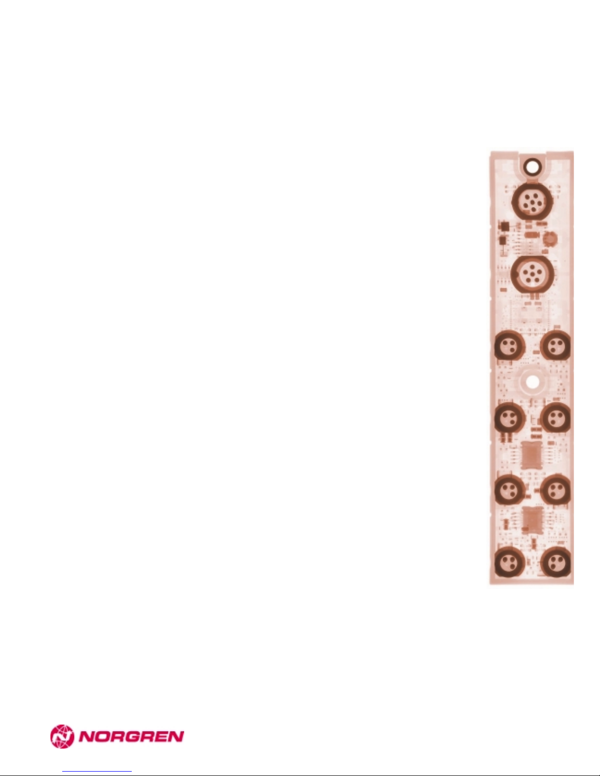
8.1 FD67NDPM127804 .....................................................................................................................61
8.2 Digital I/O modules....................................................................................................................63
8.2.1 FD67DIOM121216 ..................................................................................................................64
8.2.1.1 Identification..................................................................................................................64
Page 4

FD67 Profibus-DP Manual
8.2.1.2 Bit assignments of I/O data........................................................................................... 64
8.2.1.3 Coding of functions ....................................................................................................... 64
8.2.1.4 Parameter bytes ........................................................................................................... 65
8.2.1.5 Bit assignments of parameter bytes .............................................................................. 65
8.2.2
FD67DIOM120016 ................................................................................................................. 66
8.2.2.1 Identification ................................................................................................................. 66
8.2.2.2 Bit assignments of I/O data........................................................................................... 66
8.2.2.3 Coding of functions ....................................................................................................... 66
8.2.2.4 Parameter bytes ........................................................................................................... 67
8.2.2.5 Bit assignments of parameter bytes .............................................................................. 67
8.2.3 FD67DIM120016 .................................................................................................................... 68
8.2.3.1 Identification ................................................................................................................. 68
8.2.3.2 Bit assignments of I/O data........................................................................................... 68
8.2.3.3 Coding of functions ....................................................................................................... 68
8.2.3.4 Parameter bytes ........................................................................................................... 69
8.2.3.5 Bit assignments of parameter bytes .............................................................................. 69
8.2.4 FD67DIOM120008 ................................................................................................................. 70
8.2.4.1 Identification ................................................................................................................. 70
8.2.4.2 Bit assignments of I/O data........................................................................................... 70
8.2.4.3 Coding of functions ....................................................................................................... 70
8.2.4.4 Parameter bytes ........................................................................................................... 71
8.2.4.5 Bit assignments of parameter bytes .............................................................................. 71
8.2.5 FD67DIM120008 .................................................................................................................... 72
8.2.5.1 Identification ................................................................................................................. 72
8.2.5.2 Bit assignments of I/O data........................................................................................... 72
8.2.5.3 Coding of functions ....................................................................................................... 72
8.2.5.4 Parameter bytes ........................................................................................................... 73
8.2.5.5 Bit assignments of parameter bytes .............................................................................. 73
8.2.6
FD67DIOM080008 ................................................................................................................. 74
8.2.6.1 Identification ................................................................................................................. 74
8.2.6.2 Bit assignments of I/O data........................................................................................... 74
8.2.6.3 Coding of functions ....................................................................................................... 74
8.2.6.4 Parameter bytes ........................................................................................................... 75
8.2.6.5 Bit assignments of parameter bytes .............................................................................. 75
8.2.7
FD67DIM080008 .................................................................................................................... 76
8.2.7.1 Identification ................................................................................................................. 76
8.2.7.2 Bit assignments of I/O data........................................................................................... 76
8.2.7.3 Coding of functions ....................................................................................................... 76
8.2.7.4 Parameter bytes ........................................................................................................... 77
8.2.7.5 Bit assignments of parameter bytes .............................................................................. 77
8.3
Analogue I/O modules.............................................................................................................. 78
8.3.1 Specific characteristics........................................................................................................... 78
8.3.1.1 Smoothing (AI modules only) ........................................................................................ 78
8.3.1.2 Delta (AI modules only)................................................................................................. 78
8.3.2
FD67AIVM120004.................................................................................................................. 79
8.3.2.1 Identification ................................................................................................................. 79
8.3.2.2 I/O data ........................................................................................................................79
8.3.2.3 Parameter bytes ........................................................................................................... 80
8.3.2.4 Bit assignments of parameter bytes .............................................................................. 81
Page 5

FD67 Profibus-DP Manual
8.3.3 FD67AOVM120004.................................................................................................................82
8.3.3.1 Identification..................................................................................................................82
8.3.3.2 I/O data.........................................................................................................................82
8.3.3.3 Parameter bytes............................................................................................................83
8.3.3.4 Bit assignments of parameter bytes...............................................................................84
8.3.4
FD67AOCM120004.................................................................................................................85
8.3.4.1 Identification..................................................................................................................85
8.3.4.2 I/O data.........................................................................................................................85
8.3.4.3 Parameter bytes............................................................................................................86
8.3.4.4 Bit assignments of parameter bytes...............................................................................86
8.3.5
FD67AICM120004 ..................................................................................................................87
8.3.5.1 Identification..................................................................................................................87
8.3.5.2 I/O data.........................................................................................................................87
8.3.5.3 Parameter bytes............................................................................................................88
8.3.5.4 Bit assignments of parameter bytes...............................................................................88
8.3.6 FD67DODSC0016.......................................................................................................................89
8.3.6.1 Identification……………………………………………………………………………………….89
8.3.6.2 Bit assignments of I/O data…………………………………………………………………… 89
8.3.6.2.1 Output data ODM…………………………………………………………………………………89
8.3.6.3 Parameter bytes.................................................................................................................89
9 GLOSSARY............................................................................................................ 90
9.1 General information about the Profibus...................................................................................90
9.2
FD67 specific.............................................................................................................................91
10 INDEX OF FIGURES ........................................................................................... 92
11 INDEX OF TABLES............................................................................................. 93
Page 6

FD67 Profibus-DP Manual
1
1 Regarding this manual
This manual is intended for Profibus system planners. It contains Profibus specific properties of the FD67
system. Please refer to the System manual for general field bus information. The Technical Data Manual
contains detailed information relevant to technical data, installation and setup of the different Input/Output
modules.
User's manuals for modules of the FD67 series :
" FD67 System handbook,
" FD67 Bus system handbook Profibus
DeviceNet
" FD67 Technical manual
Take care to read the relevant instruction manuals prior to starting up the equipment. The instruction
manuals should be kept in a safe place accessible to all users at all times.
The text, illustrations, diagrams and examples presented in this manual serve solely for the purpose of
explanation, operation and use of Input/Output modules of the FD67 series.
If you should have any further reaching questions regarding the installation and set-up of the equipment
described in this manual, please don’t hesitate to contact us. We would be glad to assist you any time.
Internet : http://www.norgren.com
Norgren reserves the right to change technical specifications or contents of this manual at any time
without notice.
1.1 Chapter overview
The “Safety information” section must be read without fail prior to working with the products and the
system. This section contains information required for safe installation and handling.
The “Configuration Information“ section directs itself to system planners. It offers important information
and details relevant to successful configuration.
The chapter "Mounting and wiring" provides detailed information on mechanical and electrical installation
of the FD67 Profibus-DP node.
The chapter "Setup" is directed towards specialist personnel responsible for startup. It gives important
information for quick and easy startup in a Profibus-DP network.
The chapter "Setup example : step by step shows the setup of a simple FD67 system in a Simatic
environment.
The chapter "Diagnosis" describes visual diagnosis displays and the structure of Profibus diagnostic data.
The "Module" section refers to the structure of parameters and I/O data of the different I/O modules. y of
technical terms can be found at the end of the manual.
Page 7

FD67 Profibus-DP Manual
2
2 Safety instructions
2.1 Designated use
The devices described in this manual serve as decentralized input/output units for connection to a
Profibus-DP network.
The products described in this manual
• were developed, manufactured, inspected and documented in accordance with the applicable safety
standards. These products do not normally pose a danger to persons or property, provided that the
applicable operating and safety instructions for configuration, assembly and operation in the manner
intended are observed.
• meet the requirements set forth in the
• EMC Directive (89/336/EEC, 93/68/EEC and 93/44/EEC)
• Low Voltage Directive (73/23/EEC)
• are designed for use in industrial applications. A characteristic of the industrial environment is that
consumers are not directly connected to the public low voltage system. Extra precautions are
required for use in residential, business and commercial applications.
Warning !
This equipment has a Class A rating and can cause
radio frequency interference in residential areas. In such cases, the operator can be
asked to take appropriate precautions.
Troublefree and safe function of this equipment is guaranteed only if the conditions for proper transport,
storage, installation and assembly are observed.
The designated operation of the equipment is guaranteed only with the housing fully installed.
All devices connected to this equipment must fulfil EN 61558-2-4 and EN 61558-2-6 requirements.
Only qualified and suitably trained electrical tradesmen knowledgeable in the safety standards of
automation technology may perform configuration, installation, setup, maintenance and testing of the
equipment.
Current safety and accident prevention laws valid for a specific application must be observed in the
configuration, installation, setup, maintenance and testing of the equipment.
Only cables and accessories are allowed which meet the requirements and regulations for safety,
electromagnetic compatibility and, where applicable, telecommunication transmission equipment and
specifications.
Information concerning the type of authorized cables and accessories that can be obtained either from
Norgren or your Norgren distributor are described in this manual.
Page 8

FD67 Profibus-DP Manual
3
2.2 Qualified personnel
Requirements to be met by qualified personnel are based on qualifications profiles described in ZVEI and
VDMA guidelines.
Weiterbildung in der Automatisierungstechnik (Further training in automation technology)
Herausgeber: ZVEI und VDMA (Publisher : ZVEI and VDMA)
Maschinenbau Verlag
Posfach 71 08 64
60498 Frankfurt
Only trained electricians familiar with the contents of this manual may be allowed to install and service the
components described here.
These are understood as being persons who,
• based on their trade qualification, experience and knowledge of relev ant standards, are able to
assess the project requirements and to recognize possible hazards.
• based on extensive experience in comparable areas, possess the same level of knowledge as could
be expected of a trained tradesman.
Only Norgren technical personnel are allowed to undertake intervention in the hardware and software of
our equipment, unless the procedure is described in this manual.
Warning !
Unqualified intervention in the hardware and software of our equipment or disregard
of warnings and information provided in this manual can result in injury or serious
damage to man and/or material.
Page 9
FD67 Profibus-DP Manual
4
2.3 Explanation of symbols
2.3.1 Use of attention signs
Notes containing important information are specially marked. These are illustrated as follows :
Attention text ........
2.3.2 Use of danger signs
Danger signs are additionally marked with an enclosing frame.
CAUTION :
Disregard of safety measures may result in damage to equipment and other serious
consequences.
DANGER :
Non-compliance with the relevant safety measures poses a danger to the health
and life of the user.
2.3.3 Use of numbering in illustrations
Illustrations are numbered with white numbers on a black, round field.
Example : # Text 1......
$ Text 2......
% Text 3......
The explanatory text follows in tabular form under the same number, in direct context to the preceding
illustration.
2.3.4 Use of handling instructions
Handling instructions describe the sequence of steps during installation, setup, operation and
maintenance that must be strictly observ ed.
Figures are numbered continuously in ascending order using black numbers in round, white fields.
Example : & Instruction 1........
' Instruction 2........
( Instruction 3........
2.3.5 Use of foot notes
Supplementary information is marked with superscripted numerals (example: Text Text 1) Text Text).
These are explained in the form of footnotes beneath tables or text at the end of the page.
Page 10

FD67 Profibus-DP Manual
5
3 Configuration information
This chapter contains indications and information required for successful installation of your system in a
Profibus-DP network. General field bus information relevant to configuration, installation and operation of
FD67 systems can be found in the following manuals :
FD67 – System manual
FD67 – Technical manual
3.1 FD67 in a Profibus-DP network
FD67 is a modular I/O system designed for decentralized gathering and processing of digital and
analogue process variables. It is made up of a field bus specific bus node and field bus-oriented I/O
modules, which are connected to the bus node via internal system connection.
3.1.1 System components
Min. configuration of a Profibus-DP network :
- one or several bus masters.
- one or several slaves.
- Profibus cables and plugs to interconnect the system units.
- one ore several bus segments linked up by repeaters.
3.1.1.1 Profibus cables
Use only A-type cables, according to EN 50 170 part 8-2. Type B cables are obsolete and should
basically not be used.
Parameter A-type cable
Impedance level / Ω
135 to 165 at a frequency of 3 to 20 MHz
Operating capacity (pF/m)
≤ 30
Loop resistance (Ω/km)
≤ 110
Wire diameter (mm) > 0,64
Wire cross section (mm2) > 0,34
The wire cross section used must fit the connection possibilities on the bus connector.
Page 11
FD67 Profibus-DP Manual
6
3.1.2 General information for successful planning in a Profibus network
Up to 32 units (including repeaters) are allowed in a bus segment.
According to the selected baud rate, the extension of a Profibus segments must not exceed the max.
recommended values ; see Table 3-1.
Repeaters can be used to divide a network into several segments. So it is possible to operate more than
32 units in an extended Profibus network. However signal delays resulting from the installation of
repeaters must be considered during configuration of the system. Up to 9 repeaters can be installed
between two units.
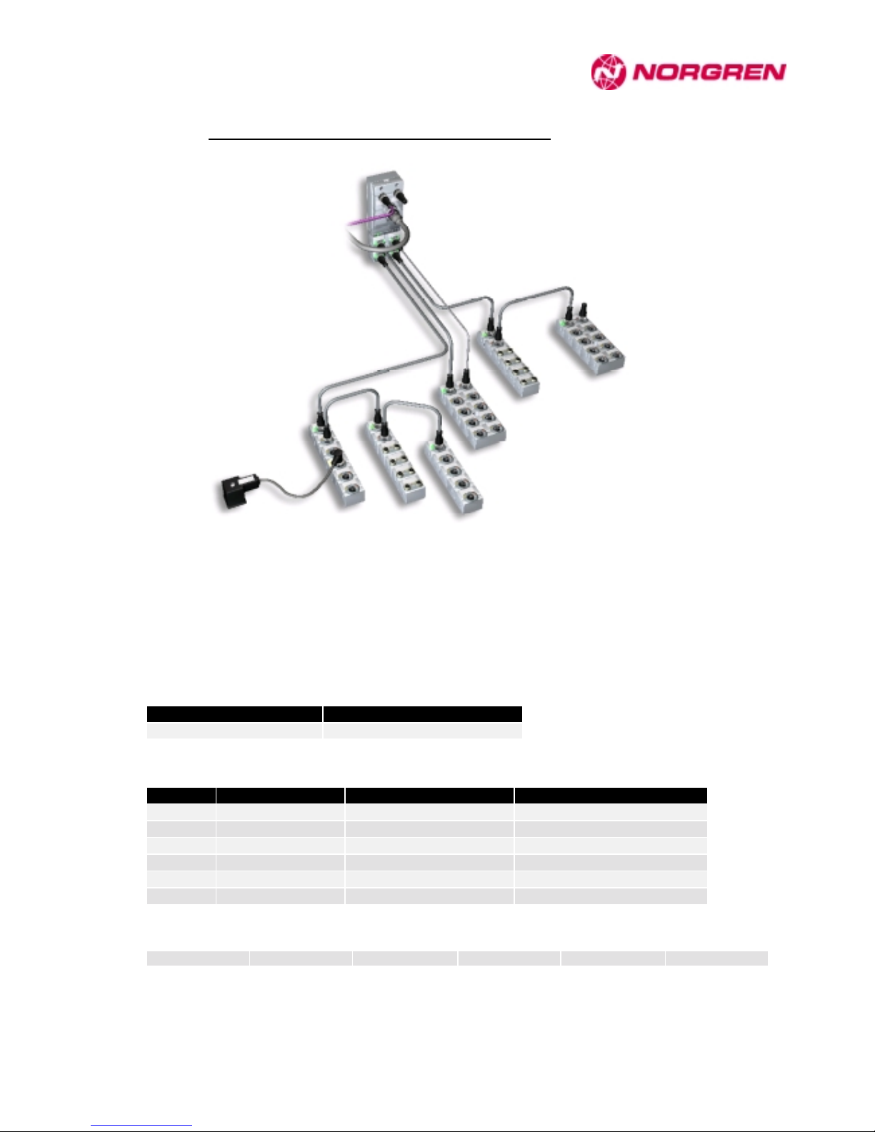
3.1.3 Topology
♦ Fig. 3-1 : Example of a Profibus network
3.1.4 Termination of bus segments
Both sides of a segment must be fitted with a terminal resistor. The terminal resistors must be supplied to
guarantee a correct physical signal level.
The terminal resistor is either located in the connector or directly integrated into the device. In both cases
it must be observed that in case of failure or application-related voltage cut-off of the unit at the end of a
segment, the terminal resistor may also be switched off to the detriment of the operatability of the whole
segment.
So it might be preferable to install be bus master at the beginning or the end of the bus segment. In case
of breakdown of the bus master, the switching off of the terminal resistor is of no importance. Additional
repeaters or externally supplied terminal resistors may be installed for reliable termination of the other
end of the segment.
The need of additional measures must be determined for ev ery specific case.
Fig. 3-1 shows an example of correct termination in a typical Profibus network.
MASTER
Slave Slave Slave Slave
Repeater
Repeater
Slave
Slave Slave Slave
Terminal resistor
Page 12

FD67 Profibus-DP Manual
7
3.1.5 Baud rate
All the devices in a Profibus network use the same baud rate set by the bus master. It is automatically
recognized by the FD67 bus node.
According to the selected baud rate, the max. admissible cable lengths must be observed (see Table 3-1
below). These values relate to a single bus segment. By using repeaters, it is possible to achieve greater
network extensions over several segments.
Baud rate in kBit/s 9,6 19,2 45,45 93,75 187,5 500 1500 3000 6000 12000
Cable length in m 1200 1200 1200 1200 1000 400 200 100 100 100
♦ Table 3-1 : Max. admissible cable lengths in a Profibus segment
3.1.6 Address
Profibus user addresses range from from 0 to 125. The two address switches of the FD67 bus node allow
to set addresses from 0 to 99.
It is important to ensure that an explicit and unique address is assigned to each Profibus user. The
Profibus address is set directly at the FD67 bus node via two BCD switches that are integrated into to the
base module.
The set address is read in once after a voltage reset. A change of address in operation is not supported.
Detailed information can be found in the FD67 System manual.
3.1.7 Spur lines
As a rule, passive spur lines should be avoided.
If spur lines are required, e.g. for temporary connection to programming or diagnostic dev ices, use active
spur lines or repeaters. Correct termination must always be assured.
3.1.8 Design guidelines
Design guidelines have been issued by the Profibus User Organization (PNO). They must be strictly
observed, as well as the information contained in the FD67 manuals. See the PNO homepage :
www.profibus.com
Page 13
FD67 Profibus-DP Manual
8
4 Mounting and wiring
Installation and wiring information relevant to I/O modules and internal system connection can be found in
the manual FD67 – Technical manual.
CAUTION :
Mounting, wiring and setting of the Profibus address must be performed while the
equipment is not under power.
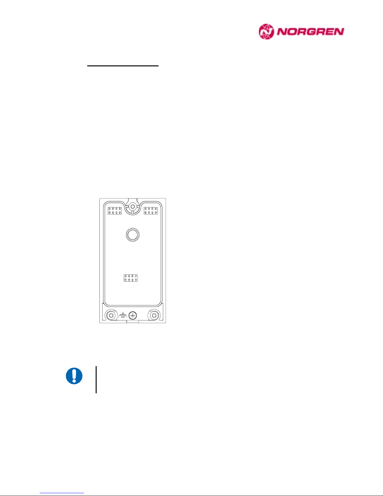
4.1 Bus node
Initial contitions
♦ Smooth and flat mounting surface.
♦ The system is dead (cut off).
Mounting material
♦ 2 fastening screws 4 mm in diameter.
♦ 2 DIN 433 T
1/T2
lock washers.
Tools
♦ Screwdriver, middle-sized
a) Mounting the base module of the bus node
Attach the module to the mounting holes by means of the 2 fastening screws 4 mm in diameter.
The tightening torque is : 2 Nm.
b) Setting the Profibus address
Two address switches are provided to set the bus node address in the Profibus network. Values
between 1 and 99 are allowable.
Two units in a Profibus network must be clearly identifiable ; therefore they must not
be allocated to the same address.
The set address is read in once after the supply voltage is applied. Therefore, a
change of address only takes effect after a module voltage reset.
Page 14
FD67 Profibus-DP Manual
9
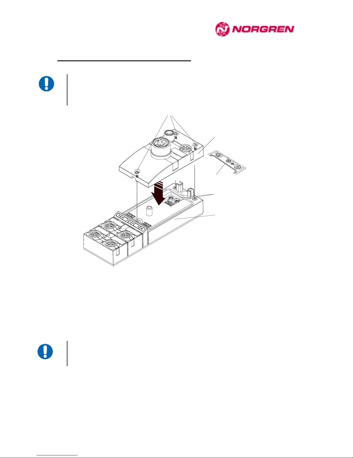
4.2 Assembling the hood of the bus node
Before assembling the hood, it is advisable to set the Profibus address, because the
switches are no more accessible when the hood is attached. It is also recommended
to note the set Profibus address on a label plate.
)
*
%
$
+
♦ Fig. 4-1 : Assembling the hood of the bus node
$ Fastening screws ) Profibus address switches
% Hood * Base module
+ Functional ground connection
& Wire the functional ground connection of the hood.
' Mount the hood on the base module.
( Screw the hood % onto the base module *. The screws are integrated into the hood $. Make sure
that the screws are equally tightened.
The hood must be screwed onto the base module and all the connectors must be
fitted with cables or blind caps in compliance with type IP 67 specifications.
Page 15
FD67 Profibus-DP Manual
10
4.3 Functional ground
Initial conditions
♦ W iring must be performed while the equipment is not under power.
Tools
♦ Screwdriver
♦ Stripper
♦ Cable terminal pliers
Accessories
♦ Fastening screw
♦ Cable terminal and locking ring
♦ Ground cable (wire)
The FE connection is located on the bottom side of the bus node hood.
$
♦ Fig. 4-2 : FE connection
$ FE connection
The connection cable of the functional ground must be kept as short as possible, in
accordance with EMC specifications.
Page 16
FD67 Profibus-DP Manual
11
4.4 Power supply
Initial conditions
Wiring must be performed while the equipment is not under power.
Tools
Stripper, screwdriver and a special tool if you do not use pre-wired conductors. Possibly a tool to screw
down the knurled ring.
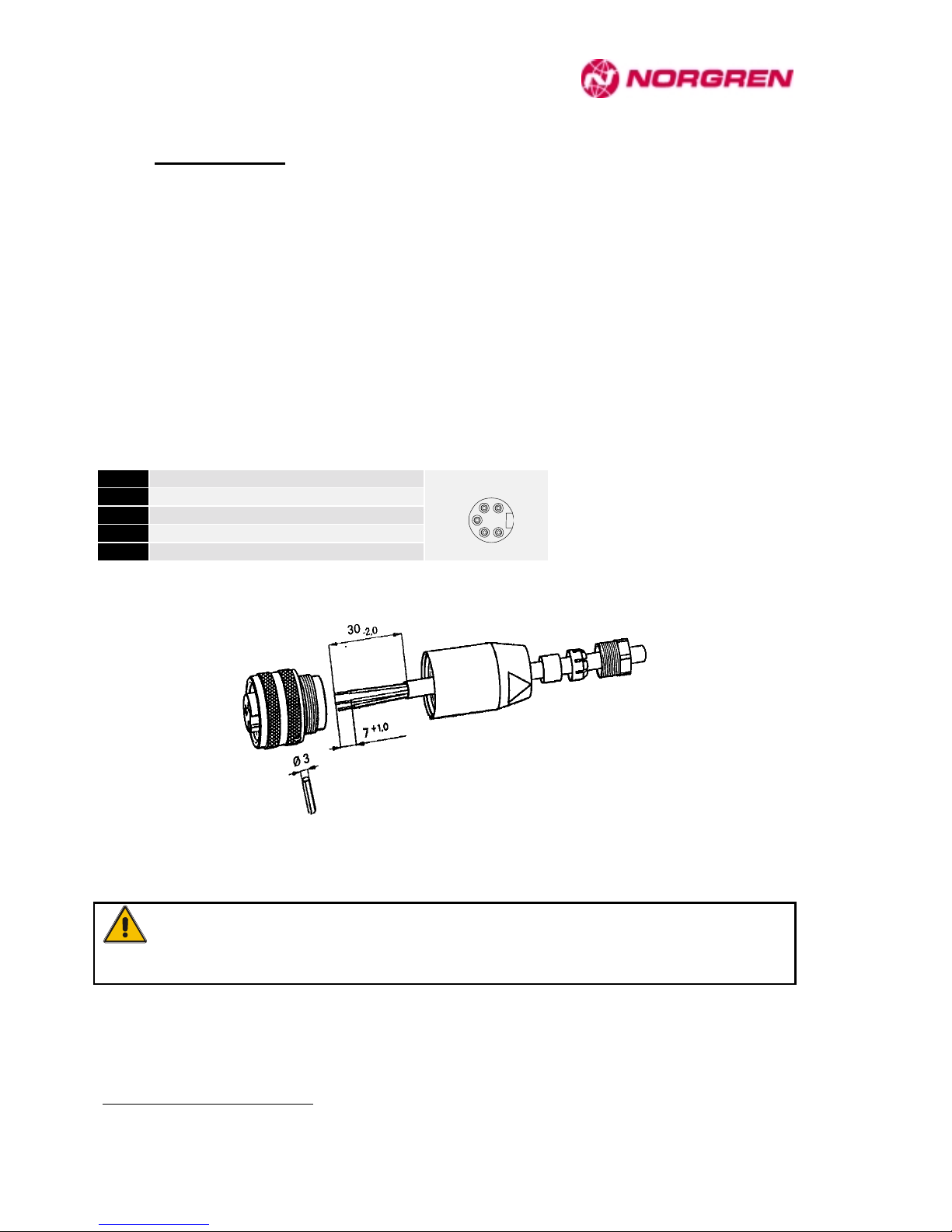
Connecting the power connector 7/8“
& Insert the plug of the power connector into the corresponding socket of the bus node. See to it that
the ends meet exactly and make sure that the plug is completely stuck into the socket.
' Screw down the plug with the knurled ring.
Pin 1 0 V1
Pin 2 0 V
Pin 3 PE
Pin 4 Sensor & Bus supply
Pin 5 Actuator supply
♦ Fig. 4-3 : Pin assignments of the 7/8“ power connector 7/8“ (Mini-Style)
♦ Fig. 4-4 : Assembly of the 7/8“ power connector (Mini-Style)
The max. admissible cable cross-section 1.5 mm². It is limited by the 7/8" connector.
CAUTION :
Reverse polarity of the power supply can damage the module.
1
The 0V reference at Pin 1 and Pin 2 is connected in the device.
POWER
12
3
4
5
Page 17
FD67 Profibus-DP Manual
12
4.5 Profibus connection
Initial conditions
Wiring must be performed while the equipment is not under power.
Tools
Stripper, screwdriver and a special tool if you do not use pre-wired conductors. Possibly a tool to screw
down the knurled ring.
Connecting the Profibus cable
& Insert the plug of the Profibus cable into the corresponding socket of the bus node. See to it that
the ends meet exactly and make sure that the plug is completely stuck into the socket.
' Screw down the plug with the knurled ring.
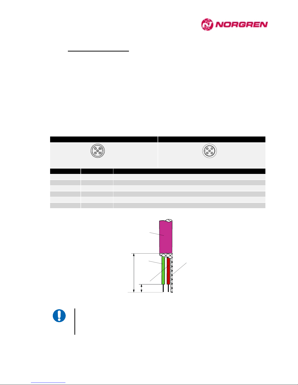
Bus In Bus Out
Contact Signal Signification
1 VP Power supply-Plus (P 5 V)
2 RxD/TxD-N RxD/TxD–N, A-line (green)
3 DGND Data transfer potential (reference potential to VP)
4 RxD/TxD-P RxD/TxD–P, B-line (red)
5 Screen Screen or ground
Thread Screen Screen or ground
♦ Fig. 4-5 : Contact assignments of Profibus M12 sockets (B-encoded)
40 mm
7 mm
%
$
+
)
♦ Fig. 4-6 : Assembling of the Profibus cable
The shield should preferably be applied over the surface of the thread. If this is not
possible, the shield can be connected via Pin 5. Both possibilities for applying the
shield can also be used together.
$ Bus cable
% Screen
+ Green line (A)
) Red line (B)
BUS IN
5
2
3
4
1
BUS OUT
1
2
3
4
5
Page 18

FD67 Profibus-DP Manual
13
4.6 Terminal resistors
Both sides of a Profibus segment must be fitted with a terminal resistor. In case of a FD67 bus node, the
terminal resistor must be installed on the connector of the extension Profibus interface of the hood.
Part No. Description
FD67K Profibus-DP terminal resistor
FD67BLKM120000 M12 x 1 FD67 blanking cap (4 pcs)
Initial conditions
- The terminal resistor must be screwed down while the system is not under power.
- The bus node is located at the beginning or at the end of a Profibus segment.
Tools
Possibly a tool to screw down the knurled ring.
Connecting the terminal resistor
& Insert the terminal resistor into the corresponding socket of the extension Profibus interface of the
hood. See to it that the ends meet exactly and make sure that the plug is completely stuck into the
socket.
' Screw down the terminal resistor with the knurled ring.
Page 19

FD67 Profibus-DP Manual
14
5 Setup
5.1 GSD file
For operation of the devices described in this manual, you require the GSD file
FD67 GSD file
The GSD file can be ordered through Norgren’s Internet homepage :
http://www.Norgren.com/
or through your branch of Norgren.
Page 20

FD67 Profibus-DP Manual
15
5.2 Allocating and setting the Profibus address
The Profibus address is set directly at the FD67 bus node via two BCD switches. Values between 1 and
99 are allowable.
The set address is read in once after the supply voltage is applied. Therefore, a
change of address only takes effect after a module voltage reset.
It is important to ensure that an explicit and unique address is assigned to each
Profibus user.
Page 21

FD67 Profibus-DP Manual
16
5.3 Configuration
Note :
The FD67 System is normally configured using a configuration tool supplied by the
master's manufacturer. Then you don't have to worry about the technical details
described in this chapter. You can find a configuration examples in Chapter 5.3.4 and
Chapter 6.
The configuration message, which defines the number of input and output bytes, is sent from the master
to the slave during the startup procedure.
FD67 uses the special ID format according to IEC 61158.
FD67 can only be operated on DP masters which support the special ID format.
Based on this information, the FD67 bus node checks the configuration for correctness. If the bus node
detects a deviation between the required configuration transferred by the DP master in the configuration
message and the actual configuration, the bus node indicates a configuration error and does not switch to
data exchange with the DP master.
The configuration error is indicated visually via the Cfg F LED on the bus node. In this
case, the Cfg F LED is lit red.
5.3.1 Placeholder
To maximize expandability of the FD67 System, it is possible to insert placeholders. A placeholder is a
module with a data length of zero and whose sole purpose is to reserve a space for adding a module at a
later date.
Note :
It is advisable to insert placeholders into the configuration for unused connectors.
See Chapter 5.3.4.2.
Page 22

FD67 Profibus-DP Manual
17
5.3.2 Structure of a configuration string
The configuration string is transmitted to the data field of the configuration message. The IDs are entered
in the order in which the modules are connected to the bus node.
Part No. Description Process data length Identification
Input Output
FD67DIOM121216 16 x Output/input M12 2 bytes 2 bytes C2
hex
01
hex
01
hex
DD
hex
18
hex
FD67DIM121216* 16 x Input M12 2 bytes - 42
hex
01
hex
DD
hex
1A
hex
FD67DOM121216* 16 x Output M12 - 2 bytes 82
hex
01
hex
DD
hex
1C
hex
FD67DIOM120016 16 x Output/input M12 2 bytes 2 bytes C2
hex
01
hex
01
hex
DD
hex
19
hex
FD67DIM120016* 16 x Input M12 2 bytes - 42
hex
01
hex
DD
hex
1B
hex
FD67DOM120016* 16 x Output M12 - 2 bytes 82
hex
01
hex
DD
hex
1D
hex
FD67DIM120016 16 x Input M12 2 bytes - 42
hex
01
hex
DD
hex
1B
hex
FD67DIOM120008 8 x Output/input M12 2 bytes 2 bytes C2
hex
01
hex
01
hex
DD
hex
23
hex
FD67DIM120008* 8 x Input M12 2 bytes - 42
hex
01
hex
DD
hex
25
hex
FD67DOM120008* 8 x Output M12 - 2 bytes 82
hex
01
hex
DD
hex
27
hex
FD67DIM120008 8 x Input M12 2 bytes - 42
hex
01
hex
DD
hex
25
hex
FD67DIOM080008 8 x Output/input M8 1 byte 1 byte C2
hex
00
hex
00
hex
DD
hex
2D
hex
FD67DIM080008* 8 x Input M8 1 byte - 42
hex
00
hex
DD
hex
2F
hex
FD67DOM080008* 8 x Output M8 - 1 byte 82
hex
00
hex
DD
hex
31
hex
FD67DIM080008 8 x Input M8 1 byte 42
hex
00
hex
DD
hex
2F
hex
FD67AIVM120004 Analogue input (voltage) M12 4 words - 42
hex
43
hex
DD
hex
7C
hex
FD67AOVM120004 Analogue output (voltage) M12 - 4 words 82
hex
43
hex
DD
hex
86
hex
FD67AOCM120004 Analogue output (current) M12 - 4 words 82
hex
43
hex
DD
hex
90
hex
FD67AICM120004 Analogue input (current) M12 4 words - 42
hex
43
hex
DD
hex
9A
hex
FD67DODSC0016 16 x Output to valve island - 2 bytes 82
hex
01
hex
DD
hex
4B
hex
♦ Table 5-1 : Profibus identifications of I/O modules
*
preconfigured module v ersions (see Chapter 5.4.2)
Page 23

FD67 Profibus-DP Manual
18
5.3.3 Replacing DI modules by DIO modules
Digital I/O modules are available in two versions :
♦ DIO : each channel can be configured as Input or Output
♦ DI : each channel is an Input
DIO modules support all the functions of corresponding DI modules. So it is possible to replace a DI
module by a DIO module without modifying the Profibus configuration.
Replaceability simplifies stock keeping of spare parts. Installing DI modules is also a cost-effective
solution.
If you replace an installed and configured DI module by a DIO module, the bus node will automatically
recognize the DIO module and assure via the integrated replacement algorithm that it behaves like a DI
module for the DP master and the application.
DI modules replaceable by DIO modules
Part No. Description Part No. Description
FD67DIM120016 16 x Input M12 FD67DIOM120016 16 x Input/output M12
FD67DIM120008 8 x Input M12 FD67DIOM120008 8 x Input/output M12
FD67DIM080008 8 x Input M8 FD67DIOM080008 8 x Input/output M8
Page 24
FD67 Profibus-DP Manual
19
5.3.4 Configuration examples
Configuration examples with hardware manager Simatic Step 7.
5.3.4.1 Configuration of compact modules
This configuration is made up of two compact modules connected to the sockets 0 and 1 of the internal
system connection of the bus node.
In this type of configuration, there is no direct relationship between the module position in the
configuration table (connector) and the actual location on the bus (string/position in the string). Instead of
connecting the modules to the sockets 0 and 1 of the bus node, you could as well connect them to the
connectors 1 and 3. You can determine the sequence and correspondence between configured modules
and modules detected by the bus node at system startup.
Note :
A simple solution consists in integrating placeholders for a better general
arrangement of the configuration and a clear relationship between the connector and
actual module position. Configuration can be easily extended at a later date by
replacing the corresponding placeholder, without any interaction on other configured
modules (e.g. they keep their module number for diagnosis).
Page 25
FD67 Profibus-DP Manual
20
5.3.4.2 Configuration with placeholders
Placeholder
Placeholder
Placeholder
Placeholder
Placeholder
Placeholder
Placeholder
Placeholder
Placeholder
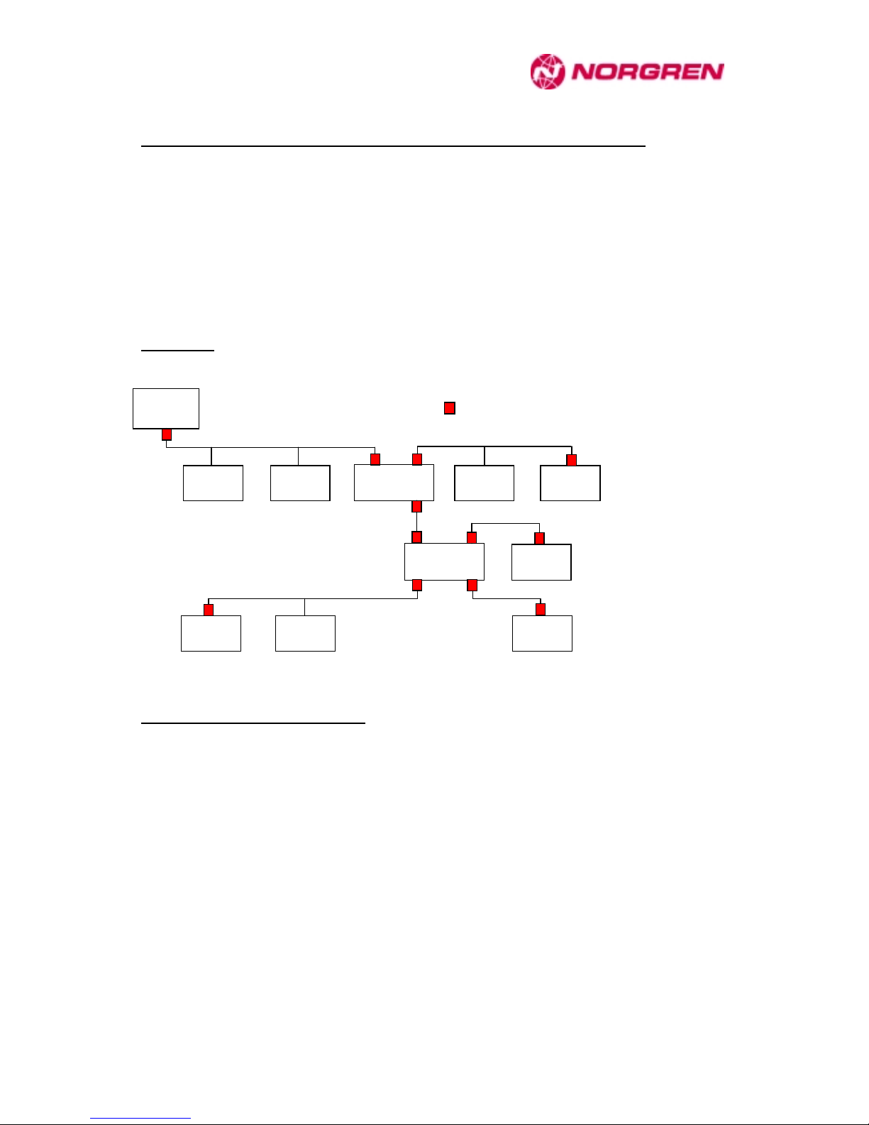
Location
Location
3 2 1 0 4 5 6 7
12 13 14 15 11 10 9 8
Placeholder
Placeholder
Placeholder
Placeholder
Placeholder
This configuration is the same as the one described in § 5.3.4.1., except that unused connectors of the
FD67 system are occupied by placeholders. Given that a maximum of 4 modules are admissible per line,
the configuration table is accordingly structured :
Page 26

FD67 Profibus-DP Manual
21
Connector Line of the internal
system connection
Module in the line Note
0 0 1
st
Module in this line
1 1 2nd Module in this line
2 2 3rd Module in this line
3
Line 0
3 4th Module in this line
4 0 1
st
Module in this line
5 1 2nd Module in this line
6 2 3rd Module in this line
7
Line 1
3 4th Module in this line
8 0 1
st
Module in this line
9 1 2nd Module in this line
10 2 3rd Module in this line
11
Line 2
3 4th Module in this line
12 0 1
st
Module in this line
13 1 2nd Module in this line
14 2 3rd Module in this line
15
Line 3
3 4th Module in this line
Examples :
The third module in line 2 is allocated to connector nb. 10.
The module allocated to connector nb. 7 is the 4th module in line 1.
Page 27
FD67 Profibus-DP Manual
22
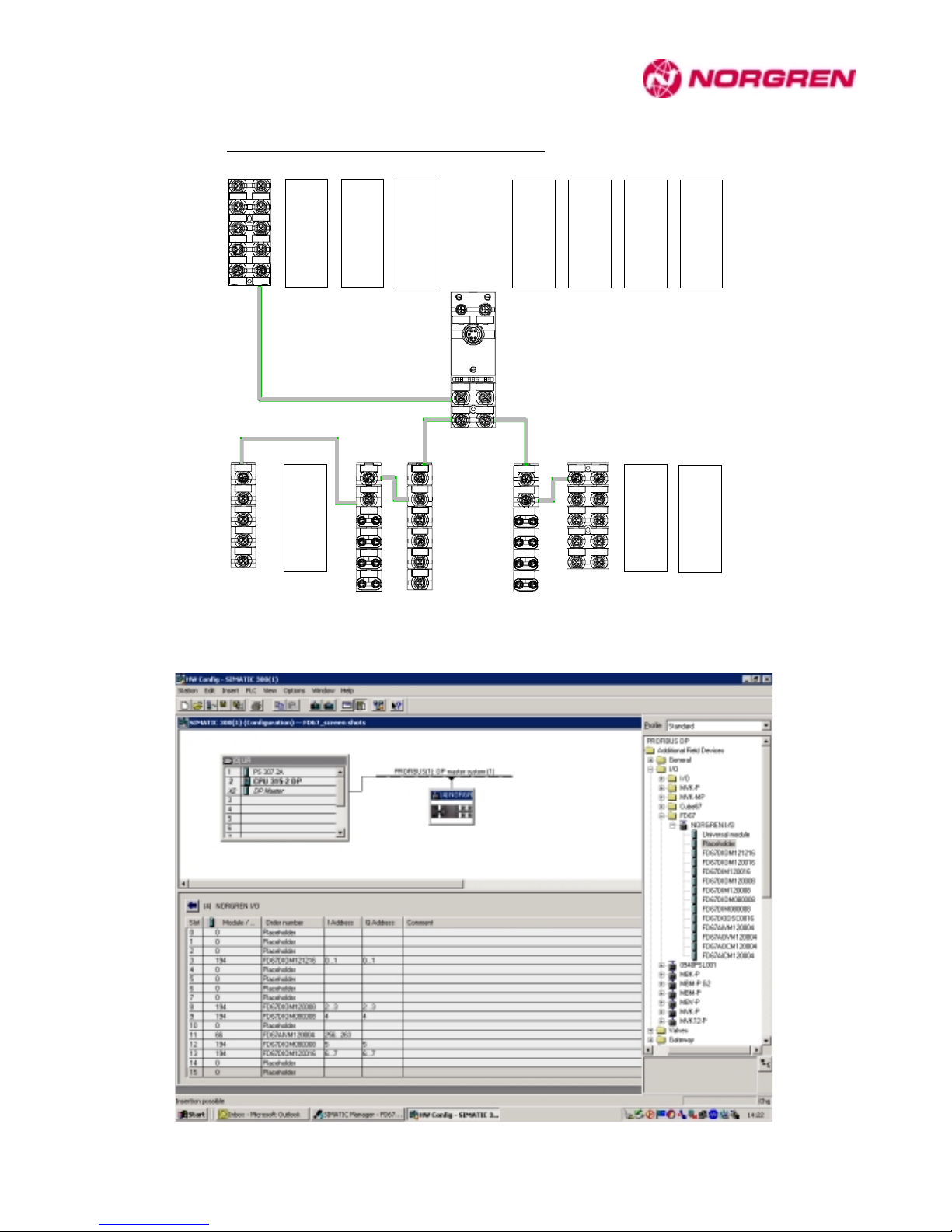
5.3.4.3 Configuration with expander modules
Placeholder
Placeholder
Placeholder
Placeholder
Placeholder
Placeholder
Placeholder
Placeholder
Placeholder
Placeholder
Location
Location
3 2 1 0 4 5 6 7
12 13 14 15 11 10 9 8
Expander modules enable the connection of up to 4 I/O modules in a line. Placeholders have been used
in this configuration example.
Page 28
FD67 Profibus-DP Manual
23
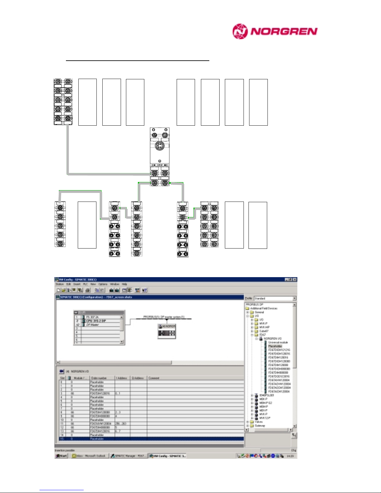
5.3.4.4 Configuration with preconfigured modules
Placeholder
Placeholder
Placeholder
Placeholder
Placeholder
Placeholder
Placeholder
Placeholder
Placeholder
Placeholder
Location
Location
3 2 1 0 4 5 6 7
12 13 14 15 11 10 9 8
Expander modules enable the connection of up to 4 I/O modules in a line. Placeholders
have been used in this configuration example.
Page 29
FD67 Profibus-DP Manual
24
5.3.4.5 Manual assembling of a configuration string
♦ Fig. 5-1 : Configuration example
The modules are automatically addressed by the bus node in the order of connection : first all the
modules connected to socket 0 of the internal system connection, then all the modules connected to
socket 1 of the internal system connection and so on.
The configurations strings of the different modules can be found in chapter 5.3.2.
1. Bus node
Module Identification
FD67NDPM127804 01
hex
51
hex
2. I/O modules
Nb/Slot Art.No Internal system connection Identification
0 FD67DIOM121216 Socket 0 C2
hex
01
hex
01
hex
DD
hex
18
hex
1 FD67DIOM120008 Socket 2 C2
hex
01
hex
01
hex
DD
hex
23
hex
2 FD67DIOM080008 Socket 2 C2
hex
00
hex
00
hex
DD
hex
2D
hex
3 FD67AOVM120004 Socket 2 82
hex
43
hex
DD
hex
86
hex
4 FD67DIOM080008 Socket 3 C2
hex
00
hex
00
hex
DD
hex
2D
hex
5 FD67DIOM120016 Socket 3 C2
hex
01
hex
01
hex
DD
hex
19
hex
3. The configuration string (all values in hexadecimal notation) looks like this :
C2,01,01,DD,18 C2,01,01,DD,23 C2,00,00,DD,2D 82,43,DD,86 C2,00,00,DD,2D C2,01,01,DD,19
The configuration software generally supports a visual configuration, so you don't have to assemble the
configuration string yourself.
FD67DIOM121216
FD67DIOM120016
FD67DIOM080008
FD67AOVM120004
FD67DIOM080008
FD67DIOM120008
FD67NDPM127804
Page 30

FD67 Profibus-DP Manual
25
5.4 Parameterisation
Parameterisation allows to define the characteristics of the FD67 system and the connected I/O modules,
e.g. :
♦ Function of an I/O channel (Input or Output)
♦ Enable/disable diagnosis and type of diagnosis.
♦ etc.
By using a graphic configuration tool, parameterisation is made easier thanks to the information contained
in the GSD file. Refer to the documentation of the configuration tool.
With the following information, you can assemble the parameter string yourself. See chapter 8 for the
coding of parameter bytes (bus node and I/O modules).
♦ Fig. 5-2 : Hardware-configurator in a Simatic S7 environment
The GSD file contains two preconfigured versions for freely configurable DIO modules.
These preconfigured versions can be used if you need only Inputs or only Outputs on this module.
See also chapter 5.4.2.
Page 31

FD67 Profibus-DP Manual
26
5.4.1 Parameter message
The master sends a parameter message to the slave. The first 7 bytes are defined by Profibus standard
IEC 61158. They are followed by user parameters. The number and composition of the user parameters
are dependent on the configuration of the FD67 System.
A plaintext message is stored in the GSD file for each parameterization function.
5.4.1.1 Structure of the standard specific parameters (bytes 0 to 6)
Byte Bit Selection
7 6 5 4 3 2 1 0
0
Lock
Req
Unlock
Req
Sync
Req
Free
Req
WD
On
res res res
Stationsstatus
1
WD_Fact_1
2
WD_Fact_2
3
MinTSDR
4
Ident_Number_High
5
Ident_Number_Low
6
Group_Ident
Byte 0
7 6 5 4 3 2 1 0
Reserved
Reserved
Reserved
WD_On = 1 , Response monitoring in slave activated
Freeze_Req = 1 , Slave in Freeze_Mode
Sync_Req = 1 , Slav e in Sync_Mode
Unlock
Lock
Lock Unlock Signification
0 0 min
TSDR
and slave specific parameters may be overwritten
0 1 DP-Slave is enabled for other masters
1 0 DP-Slave is disabled for other masters ; all parameters are accepted
1 1 DP-Slave is enabled for other masters
Byte 1
7 6 5 4 3 2 1 0
WD_Fact_1
Byte 2
7 6 5 4 3 2 1 0
WD_Fact_22
2
TWD (s) = 10ms - WD_Fact_1 - WD_FACT_2. Time to expiration of response monitoring in the DP
slave.
Page 32

FD67 Profibus-DP Manual
27
Byte 3
7 6 5 4 3 2 1 0
TSDR3
Byte 4
7 6 5 4 3 2 1 0
Identnummer Highbyte (here : 06
hex
)
Byte 5
7 6 5 4 3 2 1 0
Identnummer Lowbyte (here : 4D
hex
)
Byte 6
7 6 5 4 3 2 1 0
Group_Ident
5.4.1.2 User parameters
Standard specific parameters are followed by a number of user parameters dependent on the FD67
structure and extension. They first include parameters for the bus node and then parameter bytes for the
different modules. The sequence corresponds to the order in which the modules are connected to the bus
node. See chapter 8.
Parameterisation example : bus node and FD67DIOM121216.
Requirements :
You don't want the bus node to generate a diagnosis message if the actuator supply drops below 12 V
(Diagnosis „No Actuator supply“). If underv oltage of the actuator supply is monitored, no diagnosis
message will be generated, ev en if in case of an actuator supply cut-off caused for example by the
opening of a protection gate.
The I/O module must be parameterised as an Output at Pin 4 and as an Input with make function at Pin 2
(non-inverted input).
The user parameter string (all values in hexadecimal notation) looks like this :
Bus node I/O module FD67DIOM121216
00 00 00 82 AA AA 00 00 00 00 00 00
Reserved
Reserved
Reserved
Global settings
Function channels 00 to 03
Function channels 04 to 07
Function channels 10 to 13
Function channels 14 to 17
Reserved
Reserved
Reserved
Reserved
3
Time in Tbit until DP slave is allowed to reply at the earliest. The standard requires a value of at least
11. This value must, in any case, be less than max
TSDR
Page 33

FD67 Profibus-DP Manual
28
5.4.2 Preconfigured modules
The GSD file contains two preconfigured versions for freely configurable DIO modules.
These preconfigured versions can be used if you need only Inputs or only Outputs on this module.
Advantage of preconfigured modules :
♦ Addresses are allocated either in the IDM
4
or in the ODM5 of the PLC.
♦ Quick parameterisation during the configuration of I/O modules.
4
Input Data Map
5
Output Data Map
Page 34

FD67 Profibus-DP Manual
29
6 Setup example : step by step
6.1.1 Mechanical structure
6.1.1.1 Mounting the hood of the bus node
)
*
%
$
+
♦ Fig. 6-1 : Mounting the hood of the bus node
$ Fastening screws ) Profibus address switches
% Hood * Base module
+ FE connection
Step by step :
& Set the Profibus address using the two BCD switches ) in the base module *.
' Connect the FE cable on the bottom side + of the hood %.
( Mount the hood % onto the base module. Take care not to tilt the hood.
. Tighten the three fastening screws $ integrated into the hood.
Page 35

FD67 Profibus-DP Manual
30
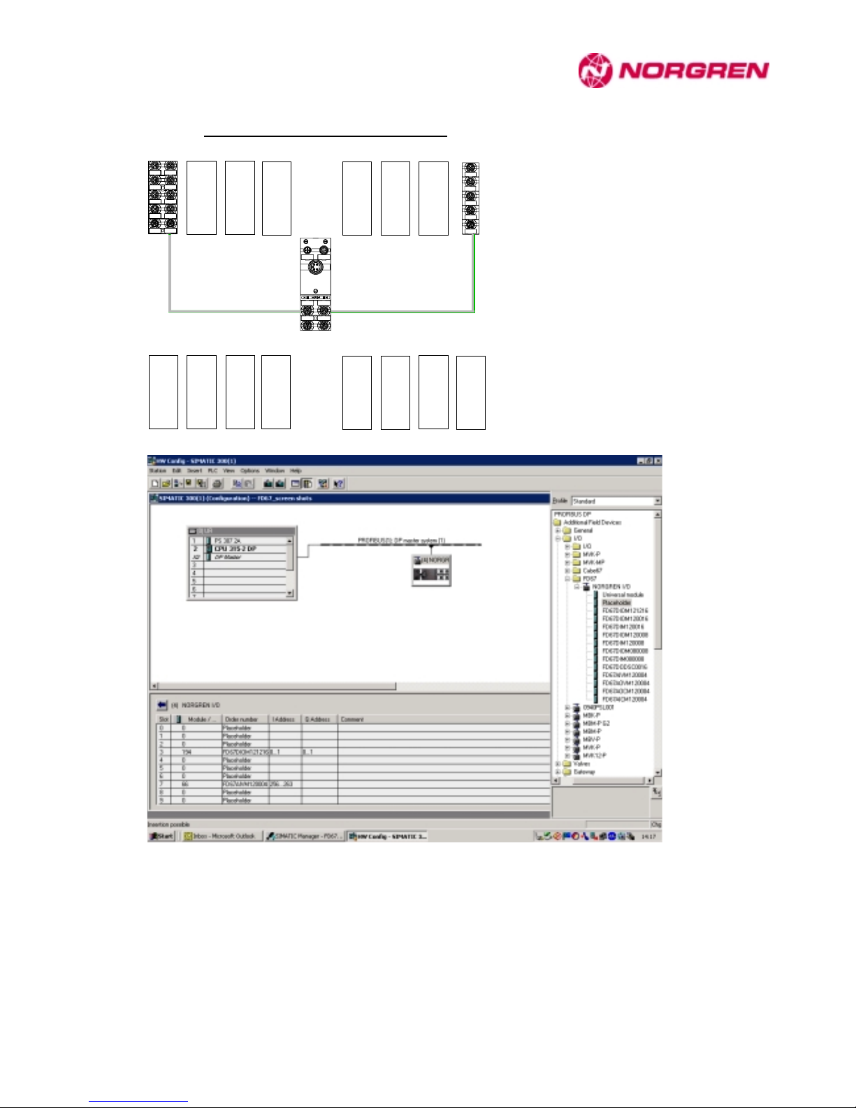
6.1.1.2 Interconnecting system components
♦ Fig. 6-2 : Interconnection of system components
$ Bus node, base module
% Bus node, hood
+ FD67AOVM120004
) Internal system connection
* Incoming Profibus line
/ Profibus terminal resistor
0 Power supply line
1 M12 lines to sensor or actuator
2 PLC
3 Power supply unit
Step by step :
& Connect the module + via the light grey system line ) to the bus node $.
' Connect M12 lines 1 to sensors or actuators to the module +.
( Connect the incoming Profibus line * to the Bus-In connection of the bus node hood %.
. Connect the outgoing Profibus line to the next Profibus user ; if the bus node is the last user in
Profibus segment, a terminal resistor / must be installed.
4 Connect the power supply 3 via the 7/8“ connector.
$
%
+
)
*
/
0
1
2
3
Master
Page 36

FD67 Profibus-DP Manual
31
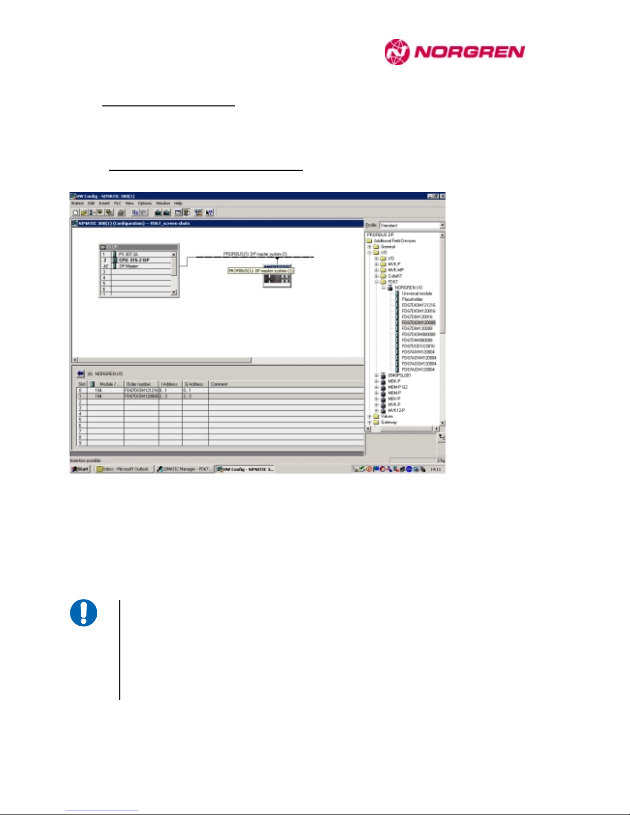
6.1.2 Configuration with S7 Hardware Manager
This chapter explains the HW configuration as an example (hardware setup software of the Simatic S7
Manager by Siemens) to show how a FD67 System is configured and parameterized.
To provide more detailed information, particularly information on diagnosis processing, would go beyond
the scope of this manual. For information, please refer to the documentation of the DP master or the
controller (PLC).
Click on the FD67 bus node
previously connected to the
Profibus to call up a table in the
lower half of the screen in which
the indiv idual modules connected
to the bus node can be entered.
In the hardware catalogue of the
Simatic Manager you will find
FD67 under “other field dev ices” >”I/O”
Mark “FD67NDPM127804” in the
hardware catalogue and drag the
entry to the Profibus with the left
mouse button pressed.
Page 37

FD67 Profibus-DP Manual
32
Allocating the Profibus address
& Double click on the bus node
' Click on “Profibus...”
( Set the address
. Close the window
Inserting an I/O module
Join the module with the
designation "FD67AOVM120004”
on the first line of the table by
dragging the module with the left
mouse button pressed.
Page 38

FD67 Profibus-DP Manual
33
Global settings
Double click on the bus node to
perform global settings under the
"Paramerisation" tab.
Module-related settings
To open the Properties dialogue of
the module, double-click the left
mouse button on the modules
specified in the table.
Module-related settings, e.g.
parameterisation of channels as
input or output, can be performed
via this dialogue.
Page 39

FD67 Profibus-DP Manual
34
7 Diagnosis
7.1.1 Behaviour in case of interrupted communication
Il the internal system connection is interrupted (communication line or sensor supply from the bus node to
the different I/O modules) the whole system is switched into fault status. Input data cannot be read any
more. The internal status of the system connection is indicated via the bus node diagnosis.
Profibus line interrupted
Bus node :
BusRun LED
Green flashing
US LED Green
Profibus diagnosis The user in not accessible
I/O module :
US LED Green
Outputs Outputs are switched off.
Internal system connection interrupted
Bus node
BusRun LED
Green flashing
US LED
Green flashing in case of communication error in this line
Profibus diagnosis In extended diagnosis, the error message "communication error" is activated for all
the modules that are no more accessible.
I/O module with sensor supply
US LED
Green flashing
Outputs Outputs are switched off.
I/O module withour sensor supply
US LED The module electronics is not supplied. All the LEDs are off.
Outputs Outputs are switched off.
The colour of the US or UA LED is dependent on the power supply status. In case of
undervoltage and communication error, the corresponding US LED flashes red.
Caution :
FD67 devices are not safety devices, as specified by the relevant standard. The Off Status of outputs must not be used to meet safety-oriented requirements of the
application !
Page 40

FD67 Profibus-DP Manual
35
7.2 LED displays
7.2.1 General information
The FD67 system is capable of detecting and reporting numerous errors. Errors are reported (Diagnosis)
via
♦ LED displays
♦ Profibus diagnosis message. See chapter 7.2.3.
7.2.2 Bus node
U
A
U
S
Bus Run
Cf g F
♦ Fig. 7-1 : LED displays on the bus node
Colour Significaton Bus Run LED Solution
Green Profibus-DP data exchange -
Green
flashing
No DP data exchange
cf. Chapter 7.5.1 Troubleshooting in a Profibus
network
Off Profibus-Firmware not yet initialised
The bus node initialisation may take a few
seconds.
♦ Table 7-1 : Status displays of the BusRun LED on the bus node
Colour Signifcation Cfg-F LED Solution
Off - -
Red
Profibus-DP configuration or
parameterisation error
cf. Chapter 7.5.1 Troubleshooting in a Profibus
network
♦ Table 7-2 : Status displays of the CfgF
6
LED on the bus node
6
CfgF = configuration fault
Page 41

FD67 Profibus-DP Manual
36
3
U
A
In Out
Bus
In Out
Bus
U
S
U
A
0
1
U
S
U
A
Bus R un
Cfg F
2
U
S
U
A
♦ Fig. 7-2 : Location of the U
S
and UA displays on the bus node
LED designation LED display 7 Behaviour Status
U
S
Lit Data exchange
U
S
Flashing No data exchange
US
Off No communication
♦ Table 7-3 : Status of the system communication on the bus node
LED designation LED display Behaviour Status
U
S
Green ok (> 18 V)
U
S
Red
Undervoltage or short-circuit
sensor supply
US
Off
No supply or
sensor supply < 12,5 V
♦ Table 7-4 : Status of sensor and system supply on the bus node
7
The display colour indicates the voltage status.
Page 42

FD67 Profibus-DP Manual
37
LED designation LED display Behaviour Status
U
A
Green ok (> 18 V)
U
A
Red
Undervoltage or short-circuit
actuator supply
UA
Off
No supply or
actuator supply < 12,5 V
♦ Table 7-5 : Status of the actuator supply on the bus node
7.2.2.1 Bus node response to faulty supply voltage
7.2.2.1.1 Short-circuit of sensor supply of internal system connection
A short-circuit at the socket or in the cable of the system connection is detected. The sensor supply, and
hence the module supply for this line, is switched off. The system goes over into communication error.
After the short-circuit has been rectified, the internal system connection can be restarted via a voltage
reset of the sensor supply. In case of inadequate power supply unit, it will be switched off before the
short-circuit detection by the bus node and will initiate a reset of the bus node. The U
S
LED on the bus
node is lit red for this line.
7.2.2.1.2 Short-circuit of actuator supply of internal system connection
A short-circuit at the socket or in the cable of the system connection is detected. The actuator supply for
this line is switched off. After the short-circuit has been rectified, it can be cleared via a voltage reset of
the actuator supply. The U
A
LED on the bus node is lit red for this line.
7.2.2.1.3 Undervoltage of sensor supply of internal system connection
Undervoltage is detected below approx. 17.0 V. The US displays of the lines affected are red. If the
voltage drops below approx. 12.5 V, the bus node goes into reset. The bus node reconnects to the
Profibus as soon as the sensor voltage rises above approx. 13.0 V.
Page 43

FD67 Profibus-DP Manual
38
7.2.3 Displays of digital I/O modules
7.2.3.1 LED displays of digital I/O modules
7.2.3.1.1 Bus IN – LED displays
U
A
U
S
♦ Fig. 7-3 : Location of the U
S
and UA displays,.
LED designation LED display8 Behaviour Status
U
S
Lit Data exchange
U
S
Flashing No data exchange9
US
Out No communication10
♦ Table 7-6 : Status of the system communication
LED designation LED display Behaviour Status
U
S
Green
ok (> 18 V)
U
S
Red Undervoltage
US
Off No supply (< 12 V)
♦ Table 7-7 : Status of the sensor and system supply (BusIn display)
8
The display colour indicates the voltage status.
9
Communcation interrupted at least in one line.
10
The module has no sensor supply.
Page 44

FD67 Profibus-DP Manual
39
LED designation LED display Behaviour Status
U
A
Green
ok (> 18 V)
U
A
Red Underv oltage
UA
Off No supply (< 12 V)
♦ Table 7-8 : Status of the internal actuator supply (BusIn display)
7.2.3.1.2 Extern Power – LED displays (FD67DIOM121216 only)
LED designation LED display Behaviour Status
U
A
Green
ok (> 18 V)
U
A
Red Underv oltage
UA
Off No supply (< 12 V)
♦ Table 7-9 : Status of the Extern Power displays (FD67DIOM121216 only)
7.2.3.1.3 M12 sockets – LED Diagnosis displays
LED display 11
Voltage
channels
00...07
Voltage
channels
10...17
Diagnosis
channels 00...07
Diagnosis
channels 10...17
0 V 0 V - External fault
0 V 0 V -
Sensor short-circuit at Pin 1
0 V 0 V - Actuator cut-off
0 V 24 V - Actuator warning
- 0 V - -
0 V 0 V
Sensor short-circuit at Pin 1
-
0 V 0 V Actuator cut-off -
24 V 0 V Actuator warning -
♦ Table 7-10 : M12 sockets – LED Diagnosis displays
11
All diagnosis displays are red.
Page 45

FD67 Profibus-DP Manual
40
7.2.3.2 Relationship between signal-logical representation and LED response
Each input and output is allocated a separate status display which is labelled '00...07' or '10...17'. It is
located next to the corresponding M12 socket ; this simplifies status assignment of peripheral
components such as sensors and actuators.
Voltage at input Logical value LED display12
0 V 0
Off
Input with make
funtion
24 V 1 Yellow
0 V 1 Off
Input with break
funtion
24 V 0 Yellow
0 V 1
Red
Diagnosis input
24 V 0
Off
♦ Table 7-11 : Relationship between signal-logical representation and LED response - Input
Logical value Voltage at output LED display
0 0 V
Off
Output
1 24 V Yellow
♦ Table 7-12 : Relationship between signal-logical representation and LED response - Output
12
If a channel-related diagnosis is available, the LED assigned to this channel is continuously lit red.
Page 46

FD67 Profibus-DP Manual
41
7.2.4 Displays of analogue I/O modules
7.2.4.1 Bus IN – LED displays
The function of the Bus IN – LED display is identical to digital modules. See chapter 7.2.3.1.1 Bus IN –
LED .
7.2.4.2 M12 sockets – LED Diagnosis displays
LED display Measured variable at input Channel-related diagnosis
- Sensor short-circuit
Higher than parameterised
measuring range
Measuring range overshoot
Lower than parameterised
measuring range
Measuring range undershoot13
Red
< 2 mA Line breakage (FD67AICM120004 only)
♦ Table 7-13 : M12 sockets – LED Diagnosis displays FD67AIVM120004 and FD67AICM120004
LED display Set-point at output Channel-related diagnosis
- Sensor short-circuit
< 0,3 % from measuring range
threshold
Short-circuit (FD67AOVM120004 only)
Red
> 2 mA Line breakage (FD67AOCM120004 only)
♦ Table 7-14 : M12 sockets – LED Diagnosis displays FD67AOVM120004 and FD67AOCM120004
13
Operation mode –10 V...+10 V, or 4 mA...20 mA only.
Page 47

FD67 Profibus-DP Manual
42
7.2.5 Power distributor displays
LED display Voltag at output Status
Off 0 V No power supply connected
Green Present Power supply connected
Red 0 V Short-circuit at output
♦ Table 7-15 : 6-pin M12 sockets – LED displays
Undervoltage detection is not supported by the power distributor. Undervoltage diagnosis is performed in
the module supplied by the voltage drawn from the power distributor.
♦ Fig. 7-4 : Location of the power distributor displays
Page 48

FD67 Profibus-DP Manual
43
7.3 Profibus
Diagnosis status modification of the FD67 System is reported to the DP master. The DP master then
requests the diagnostic information, which is supplied in the form of the diagnosis message described
below.
Some DP masters accept in standard configuration only diagnosis messages with a
maximum length of 32 bytes. If possible, this value should be set to the maximum
Profibus-DP supported length of 244 bytes. Otherwise, the max. length must be
limited by blinding channel-related diagnosis messages (Bus node parameters, see
chapter 8). In this case, a channel-related diagnosis is only reported in the form of a
collective bit in the station-related diagnosis.
The diagnosis model of Profibus DP distinguishes between three layers of diagnostic information.
A plaintext message is stored in the GSD file for each diagnosis. Diagnosis messages can be masked out
selectively v ia the bus node parameterization.
Example :
In an application, the actuator supply voltage is to be monitored for undervoltage, but no diagnosis is to
be generated when the actuator v oltage is switched off, e.g. in an emergency stop situation.
Solution :
The parameter "No actuator supply" of the bus node is set to "Do not report'.
Result :
No diagnosis is generated if the actuator supply v oltage is less than 12 V. If the voltage is between 12 V
and 18 V, the diagnosis "Undervoltage actuator supply" will be reported.
Station-related diagnosis
- Undervoltage measured at bus node
- Undervoltage measured at I/O module
- Communication fault
- etc.
ID-related diagnosis
- Information as to which modules have diagnostic capability
Channel-related diagnosis
- Short-circuit in the supply of a sensor
- Short-circuit to 0V or overload (actuator cut-off)
- Short-circuit to +24 V (actuator warning)
- Diagnosis according to DESINA
- etc.
Page 49

FD67 Profibus-DP Manual
44
7.3.1 Diagnosis Overflow
The FD67 bus node can process up to 32 channel-related diagnosis messages and report them to the DP
master. In presence of more than 32 channel-related diagnosis, the Diag.ext_overflow bit (standard
diagnotic information, byte 2) is set in the DP diagnosis message.
♦ Fig. 7-5 : Max. number of channel-related diagnosis
Station-related diagnosis includes one module-related diagnosis byte for each I/O module.
Bytes 10 to 25 Module-related diagnosis (1 byte for each module)
7 6 5 4 3 2 1 0
U
U
U
n
n
n
d
d
d
e
e
e
r
r
r
v
v
v
o
o
o
l
l
l
t
t
t
a
a
a
g
g
g
e
e
e
s
s
s
e
e
e
n
n
n
s
s
s
o
o
o
r
r
r
s
s
s
u
u
u
p
p
p
p
p
p
l
l
l
y
y
y
N
N
N
o
o
o
s
s
s
e
e
e
n
n
n
s
s
s
o
o
o
r
r
r
s
s
s
u
u
u
p
p
p
p
p
p
l
l
l
y
y
y
U
U
U
n
n
n
d
d
d
e
e
e
r
r
r
v
v
v
o
o
o
l
l
l
t
t
t
a
a
a
g
g
g
e
e
e
a
a
a
c
c
c
t
t
t
u
u
u
a
a
a
t
t
t
o
o
o
r
r
r
s
s
s
u
u
u
p
p
p
p
p
p
l
l
l
y
y
y
N
N
N
o
o
o
a
a
a
c
c
c
t
t
t
u
u
u
a
a
a
t
t
t
o
o
o
r
r
r
s
s
s
u
u
u
p
p
p
p
p
p
l
l
l
y
y
y
U
U
U
n
n
n
d
d
d
e
e
e
r
r
r
v
v
v
o
o
o
l
l
l
t
t
t
a
a
a
g
g
g
e
e
e
e
e
e
x
x
x
t
t
t
e
e
e
r
r
r
n
n
n
a
a
a
l
l
l
a
a
a
c
c
c
t
t
t
u
u
u
a
a
a
t
t
t
o
o
o
r
r
r
s
s
s
u
u
u
p
p
p
p
p
p
l
l
l
y
y
y
N
N
N
o
o
o
e
e
e
x
x
x
t
t
t
e
e
e
r
r
r
n
n
n
a
a
a
l
l
l
a
a
a
c
c
c
t
t
t
u
u
u
a
a
a
t
t
t
o
o
o
r
r
r
s
s
s
u
u
u
p
p
p
p
p
p
l
l
l
y
y
y
Channel-related diagnosis
C
C
C
o
o
o
m
m
m
m
m
m
u
u
u
n
n
n
i
i
i
c
c
c
a
a
a
t
t
t
i
i
i
o
o
o
n
n
n
f
f
f
a
a
a
u
u
u
l
l
l
t
t
t
The collective bit „Channel-related diagnosis" is set only in presence of at least one channel-related
diagnosis for the I/O module and
if it belongs to the 32 channel-related diagnosis messages that can be
reported.
This is also the case if the channel-related diagnosis has been masked out via the bus node
parameterisation. The Diag.ext_ov erflow bit is set in both cases.
Max. 32 channel-related diagnosis
A
dditional diagnostic information are
displayed via the LEDs on the I/O modules ;
they are not reported in the DP diagnosi
s
message.
Page 50

FD67 Profibus-DP Manual
45
7.3.2 Structure of a diagnosis message
The diagnostic information comprises standard diagnostic information (6 bytes) and manufacturer-specific
diagnostic information.
7.3.2.1 Bytes 0 to 5 : standard diagnostic information
Byte 0
7 6 5 4 3 2 1 0
Diag.station_non_existent
This bit is set by the DP master if this DP slave is not accessible (for generation of a
collective diagnosis). The DP slave sets this bit to zero.
Diag.station_not_ready
This bit is set by the DP slave if the DP slave is not ready for data exchange.
Diag.cfg_Fault
This bit is set by the DP slave as soon as the configuration data previously received from
the master does not match the configuration data ascertained by the DP slave.
Diag.ext_diag
This bit indicates that a diagnostic entry is present in the slave specific diagnosis area
(Ext_Diag_Data).
Diag.not supported
This bit is set by the DP slave as soon as a function not supported by the DP slave is
requested.
Diag.Invalid slave response
This bit is set by the DP master as soon as an implausible response is received from an
addressed DP slave. The DP slave sets this bit to zero.
Diag.prm_fault
This bit is set by the DP slave if the previous parameter message was erroneous, e.g.
incorrect length, incorrect ID number, invalid parameter.
Diag.master_lock
The DP slave has been parameterized by another master. This bit is set by the requester if
address in byte 3 is not equal to FF
hex
and not equal to own address. The DP slave sets this
bit to zero.
Page 51

FD67 Profibus-DP Manual
46
Byte 1
7 6 5 4 3 2 1 0
Diag.Prm_req
If the DP slave sets this bit, it must be re-parameterized and re-configured. The bit remains
set until a parameterization is finished.
Diag.Stat_diag
If the DP slave sets this bit, the DP master must get diagnostic data until this bit is deleted.
The DP slave sets this bit when it cannot provide valid user data, for instance.
Set to 1
Diag.WD_ON
If this bit is set to 1, response monitoring is activated.
Diag.freeze_mode
This bit is set by the DP slave as soon as it receives the Freeze command.
Sync_mode
This bit is set by the DP slave as soon as it receives the Sync command.
Diag.Not_Present
This bit is set by the DP master for the DP slaves not contained in the master parameter
block. The DP slave sets this bit to zero.
Diag.deactivated
This bit is set by the DP master as soon as the DP slave is removed from the master
parameter block of the DP master. The DP slave always sets this bit to zero.
Byte 2
7 6 5 4 3 2 1 0
Reserved
Diag.ext_overflow
If this bit is set, there is more diagnostic information available than is specified in
Ext_Diag_Data. For example, the DP slave sets this bit when there is more channel
diagnostic information available than the DP slave can enter into its send buffer. The DP
master sets this bit when the DP slave sends more diagnostic information than the DP
master can take into account in its diagnostic buffer.
Byte 3
7 6 5 4 3 2 1 0
Diag.master_add
The address of the DP master which has parameterized the DP slave is entered into this
byte. If the DP slave is not parameterized by a DP master, the DP slave sets the address
FF
hex
in this byte.
Byte 4
7 6 5 4 3 2 1 0
ID number of highbyte (here : 06
hex
)
Byte 5
7 6 5 4 3 2 1 0
ID number of lowbyte (here : 4D
hex
)
Page 52

FD67 Profibus-DP Manual
47
7.3.2.2 Station-related diagnosis bytes 6 to 25
Byte 6 Device-related diagnosis - header byte
7 6 5 4 3 2 1 0
Block length in bytes, incl. header byte. Here : 14
hex
/ 20
dez
Reserved for 00
7.3.2.2.1 System-wide diagnosis bytes 7 to 9
Byte 7 Bus node
7 6 5 4 3 2 1 0
Undervoltage bus node supply
Reserved
Reserved
Reserved
Reserved
Reserved
Reserved
Reserved
Byte 8 System voltages
7 6 5 4 3 2 1 0
Undervoltage sensor supply line 0 / 2
No sensor supply line 0 / 2
Undervoltage sensor supply line 1 / 3
No sensor supply line 1 / 3
Undervoltage actuator supply line 0 / 2
No actuator supply line 0 / 2
Undervoltage actuator supply line 1 / 3
No actuator supply line 1 / 3
Page 53

FD67 Profibus-DP Manual
48
Byte 9 Short-circuit / overload system voltages
7 6 5 4 3 2 1 0
Short-circuit sensor supply line 0
Short-circuit sensor supply line 1
Short-circuit sensor supply line 2
Short-circuit sensor supply line 3
Short-circuit sensor supply line 0
Short-circuit sensor supply line 1
Short-circuit sensor supply line 2
Short-circuit sensor supply line 3
Page 54

FD67 Profibus-DP Manual
49
7.3.2.2.2 Module-related diagnosis bytes 10 to 25
If placeholders have been inserted into the configuration, they are also counted when numbering modulerelated diagnosis messages.
Byte 10 Module 0
7 6 5 4 3 2 1 0
Undervoltage sensor supply
No sensor supply
Undervoltage actuator supply
No actuator supply
Undervoltage external actuator supply
No external actuator supply
Channel-related diagnosis
Communication fault
Byte 11 Module 1
7 6 5 4 3 2 1 0
Undervoltage sensor supply
No sensor supply
Undervoltage actuator supply
No actuator supply
Undervoltage external actuator supply
No external actuator supply
Channel-related diagnosis
Communication fault
Page 55

FD67 Profibus-DP Manual
50
Byte 12 Module 2
7 6 5 4 3 2 1 0
Undervoltage sensor supply
No sensor supply
Undervoltage actuator supply
No actuator supply
Undervoltage external actuator supply
No external actuator supply
Channel-related diagnosis
Communication fault
Byte 13 Module 3
7 6 5 4 3 2 1 0
Undervoltage sensor supply
No sensor supply
Undervoltage actuator supply
No actuator supply
Undervoltage external actuator supply
No external actuator supply
Channel-related diagnosis
Communication fault
Byte 14 Module 4
7 6 5 4 3 2 1 0
Undervoltage sensor supply
No sensor supply
Undervoltage actuator supply
No actuator supply
Undervoltage external actuator supply
No external actuator supply
Channel-related diagnosis
Communication fault
Page 56

FD67 Profibus-DP Manual
51
Byte 15 Module 5
7 6 5 4 3 2 1 0
Undervoltage sensor supply
No sensor supply
Undervoltage actuator supply
No actuator supply
Undervoltage external actuator supply
No external actuator supply
Channel-related diagnosis
Communication fault
Byte 16 Module 6
7 6 5 4 3 2 1 0
Undervoltage sensor supply
No sensor supply
Undervoltage actuator supply
No actuator supply
Undervoltage external actuator supply
No external actuator supply
Channel-related diagnosis
Communication fault
Byte 17 Module 7
7 6 5 4 3 2 1 0
Undervoltage sensor supply
No sensor supply
Undervoltage actuator supply
No actuator supply
Undervoltage external actuator supply
No external actuator supply
Channel-related diagnosis
Communication fault
Page 57

FD67 Profibus-DP Manual
52
Byte 18 Module 8
7 6 5 4 3 2 1 0
Undervoltage sensor supply
No sensor supply
Undervoltage actuator supply
No actuator supply
Undervoltage external actuator supply
No external actuator supply
Channel-related diagnosis
Communication fault
Byte 19 Module 9
7 6 5 4 3 2 1 0
Undervoltage sensor supply
No sensor supply
Undervoltage actuator supply
No actuator supply
Undervoltage external actuator supply
No external actuator supply
Channel-related diagnosis
Communication fault
Byte 20 Module 10
7 6 5 4 3 2 1 0
Undervoltage sensor supply
No sensor supply
Undervoltage actuator supply
No actuator supply
Undervoltage external actuator supply
No external actuator supply
Channel-related diagnosis
Communication fault
Page 58

FD67 Profibus-DP Manual
53
Byte 21 Module 11
7 6 5 4 3 2 1 0
Undervoltage sensor supply
No sensor supply
Undervoltage actuator supply
No actuator supply
Undervoltage external actuator supply
No external actuator supply
Channel-related diagnosis
Communication fault
Byte 22 Module 12
7 6 5 4 3 2 1 0
Undervoltage sensor supply
No sensor supply
Undervoltage actuator supply
No actuator supply
Undervoltage external actuator supply
No external actuator supply
Channel-related diagnosis
Communication fault
Byte 23 Module 13
7 6 5 4 3 2 1 0
Undervoltage sensor supply
No sensor supply
Undervoltage actuator supply
No actuator supply
Undervoltage external actuator supply
No external actuator supply
Channel-related diagnosis
Communication fault
Page 59

FD67 Profibus-DP Manual
54
Byte 24 Module 14
7 6 5 4 3 2 1 0
Undervoltage sensor supply
No sensor supply
Undervoltage actuator supply
No actuator supply
Undervoltage external actuator supply
No external actuator supply
Channel-related diagnosis
Communication fault
Byte 25 Module 15
7 6 5 4 3 2 1 0
Undervoltage sensor supply
No sensor supply
Undervoltage actuator supply
No actuator supply
Undervoltage external actuator supply
No external actuator supply
Channel-related diagnosis
Communication fault
Page 60

FD67 Profibus-DP Manual
55
7.3.2.3 ID-related diagnosis bytes 26 to 28
Byte 26 ID-related diagnosis - header byte
7 6 5 4 3 2 1 0
Block length in bytes, incl. header byte. Here : 03
hex
/ 03
dez
Reserved for 01
Byte 27 ID
7 6 5 4 3 2 1 0
Module 0 has diagnosis
Module 1 has diagnosis
Module 2 has diagnosis
Module 3 has diagnosis
Module 4 has diagnosis
Module 5 has diagnosis
Module 6 has diagnosis
Module 7 has diagnosis
Byte 28 ID
7 6 5 4 3 2 1 0
Module 8 has diagnosis
Module 9 has diagnosis
Module 10 has diagnosis
Module 11 has diagnosis
Module 12 has diagnosis
Module 13 has diagnosis
Module 14 has diagnosis
Module 15 has diagnosis
Page 61

FD67 Profibus-DP Manual
56
7.3.2.4 Channel-related diagnosis bytes 29 to 31 and following
Three bytes are assigned in the diagnosis message for each channel-related diagnosis. If, for example, 5
channel-related diagnosis are available, a total of 5 * 3 = 15 bytes of channel-related diagnostic
information.
Byte 29 ID number
7 6 5 4 3 2 1 0
ID number 0..63
Reserved for 10
Byte 30 Channel number
7 6 5 4 3 2 1 0
Reserved for 0..63. FD67 : 00..07 (Pin 4) or 10..17 (Pin 2)
Input/output
00 = reserved
01 = input
10 = output
11 = input/output
Byte 31 Fault type
7 6 5 4 3 2 1 0
Fault type (see Chapter 8.3.6)
01
hex
(01
dez
) Short-circuit (in sensor supply)
06
hex
(06
dez
) Line breakage
07
hex
(07
dez
) Up per t hres hold overs hot
08
hex
(08
dez
) Lower threshold undershot
17
hex
(23
dez
) Ac tuator war ning
18
hex
(24
dez
) Actuator cut-off
1A
hex
(26
dez
) External fault
Input/output
000 = reserved
001 = bit
010 = 2 bits
011 = 4 bits
100 = byte
101 = word
110 = 2 words
111 = reserved
Page 62

FD67 Profibus-DP Manual
57
7.3.2.4.1 Examples of channel-related diagnosis
This example refers to module number 0. If the module number is different, then the 1
st
byte will be
accordingly higher (81hex, 82hex...).
Short-circuit in sensor supply
Channel 1st
byte
2nd
byte
3rd
byte
00 – Pin 4 Sock. 0 80
hex
40
hex
21
hex
01 – Pin 4 Sock. 1 80
hex
41
hex
21
hex
02 – Pin 4 Sock. 2 80
hex
42
hex
21
hex
03 – Pin 4 Sock. 3 80
hex
43
hex
21
hex
04 – Pin 4 Sock. 4 80
hex
44
hex
21
hex
05 – Pin 4 Sock. 5 80
hex
45
hex
21
hex
06 – Pin 4 Sock. 6 80
hex
46
hex
21
hex
07 – Pin 4 Sock. 7 80
hex
47
hex
21
hex
10 – Pin 2 Sock. 0 80
hex
4A
hex
21
hex
11 – Pin 2 Sock. 1 80
hex
4B
hex
21
hex
12 – Pin 2 Sock. 2 80
hex
4C
hex
21
hex
13 – Pin 2 Sock. 3 80
hex
4D
hex
21
hex
14 – Pin 2 Sock. 4 80
hex
4E
hex
21
hex
15 – Pin 2 Sock. 5 80
hex
4F
hex
21
hex
16 – Pin 2 Sock. 6 80
hex
50
hex
21
hex
17 – Pin 2 Sock. 7 80
hex
51
hex
21
hex
Actuator cutoff
Channel 1st
byte
2nd
byte
3rd
byte
00 – Pin 4 Sock. 0 80
hex
80
hex
38
hex
01 – Pin 4 Sock. 1 80
hex
81
hex
38
hex
02 – Pin 4 Sock. 2 80
hex
82
hex
38
hex
03 – Pin 4 Sock. 3 80
hex
83
hex
38
hex
04 – Pin 4 Sock. 4 80
hex
84
hex
38
hex
05 – Pin 4 Sock. 5 80
hex
85
hex
38
hex
06 – Pin 4 Sock. 6 80
hex
86
hex
38
hex
07 – Pin 4 Sock. 7 80
hex
87
hex
38
hex
10 – Pin 2 Sock. 0 80
hex
8A
hex
38
hex
11 – Pin 2 Sock. 1 80
hex
8B
hex
38
hex
12 – Pin 2 Sock. 2 80
hex
8C
hex
38
hex
13 – Pin 2 Sock. 3 80
hex
8D
hex
38
hex
14 – Pin 2 Sock. 4 80
hex
8E
hex
38
hex
15 – Pin 2 Sock. 5 80
hex
8F
hex
38
hex
16 – Pin 2 Sock. 6 80
hex
90
hex
38
hex
17 – Pin 2 Sock. 7 80
hex
91
hex
38
hex
Actuator warning
Channel 1st
byte
2nd
byte
3rd
byte
00 – Pin 4 Sock. 0 80
hex
80
hex
37
hex
01 – Pin 4 Sock. 1 80
hex
81
hex
37
hex
02 – Pin 4 Sock. 2 80
hex
82
hex
37
hex
03 – Pin 4 Sock. 3 80
hex
83
hex
37
hex
04 – Pin 4 Sock. 4 80
hex
84
hex
37
hex
05 – Pin 4 Sock. 5 80
hex
85
hex
37
hex
06 – Pin 4 Sock. 6 80
hex
86
hex
37
hex
07 – Pin 4 Sock. 7 80
hex
87
hex
37
hex
10 – Pin 2 Sock. 0 80
hex
8A
hex
37
hex
11 – Pin 2 Sock. 1 80
hex
8B
hex
37
hex
12 – Pin 2 Sock. 2 80
hex
8C
hex
37
hex
13 – Pin 2 Sock. 3 80
hex
8D
hex
37
hex
14 – Pin 2 Sock. 4 80
hex
8E
hex
37
hex
15 – Pin 2 Sock. 5 80
hex
8F
hex
37
hex
16 – Pin 2 Sock. 6 80
hex
90
hex
37
hex
17 – Pin 2 Sock. 7 80
hex
91
hex
37
hex
External fault
Channel 1st
byte
2nd
byte
3rd
byte
10 – Pin 2 Sock. 0 80
hex
4A
hex
3A
hex
11 – Pin 2 Sock. 1 80
hex
4B
hex
3A
hex
12 – Pin 2 Sock. 2 80
hex
4C
hex
3A
hex
13 – Pin 2 Sock. 3 80
hex
4D
hex
3A
hex
14 – Pin 2 Sock. 4 80
hex
4E
hex
3A
hex
15 – Pin 2 Sock. 5 80
hex
4F
hex
3A
hex
16 – Pin 2 Sock. 6 80
hex
50
hex
3A
hex
17 – Pin 2 Sock. 7 80
hex
51
hex
3A
hex
Page 63

FD67 Profibus-DP Manual
58
7.4 Evaluation of the diagnosis message in the PLC
Access to the data of the diagnosis message is dependent on the DP master used. Please refer to the
relevant documentation.
Siemens offers functional modules for its PLCs, that facilitate data evaluation. They can be ordered
through Siemens's Internet homepage.
7.5 Troubleshooting
This chapter describes possible errors/faults and useful information for error correction.
Page 64

FD67 Profibus-DP Manual
59
7.5.1 Troubleshooting in a Profibus network
The table below shows the most current errors in a Profibus network. This list is not exhaustive. To check correct installation, there are many useful
diagnostic tools (line tester, Prof ibus tester, Prof ibus monitor) offered by different manufacturers.
Error DP Diagnosis LED Display Possible cause Solution
The unit is not supplied. Supply the unit.
No address is set or invalid address. Set correct address.
The set address is already used. A n explicit and unique address must be allocated to each Profibus user.
The t ermin al resi stor between m aster and
unit is switched on.
W hen the termin al res istor is s witched on in a Pr ofibu s c onnect or, th e next us er is
disconnected from the Profibus. Make sure that only the terminal resistors located
at both ends of the Profibus segmen t are s wiitc hed on.
W rong t erminat ion of the Pr ofib us s egment.
Both ends of a Profibus s egment must be fitted with a terminal resistor. If low
baud rates are used, the network can apparently be operated despite wrong
termi nation . Th is may c ause s porad ic f aults in pr oduc tion oper ation.
Spur lines
Baud rates up to 1.5 MBit/s max. 6.6 m
If higher baud rates are used, spur lines are
not admissible.
If s pur lines cannot be avoided , pref erably use s pecif ic „act ive“ sp ur li nes or
repeater s. P lease n ote that the num ber of repeater s us ed in a s egment is li mited .
Refer to th e relevant docum entation of th e repeater .
Unit not accessible or
communication error
No sl ave reply
Flashing BusRun LED
on bus node.
If the module is not
supplied, all the LEDs
are off .
Extens ion of the P rofi bus s egment too
large.
Admissible cable length, see table below.
Use repeaters to divide large segments into several segments.
Planned modules are diff erent from actually
installed modules.
Chec k that planned modules are actuall y presen t and c orrec tly c onnect ed to th e
bus node.
Parameterisation or
configuration error
Standard specific
diagnosis
Diag.PrmFault bit
or
Diag.CfgFault bit
is set.
- Flashing BusRun LED
on bus node.
- CfgF LED is red on
bus node
Err or in t he inter nal s ystem c onnec tion See chap ter 7. 5.2.
Connection to the DP
mast er interrup ted in
operati on
No slave reply Flashing BusRun LED.
Short-circuit or interruption in the Profibus
line.
Chec k the P rofi bus l ine.
Check which units are still accessible to locate the error.
(Preferably use the system with lower baud rate)
♦ Table 7-16 : Troubleshooting in a Profibus network
Baud rate in kBit/s 9,6 19,2 45,45 93,75 187,5 500 1500 3000 6000 12000
Cable lengths in m 1200 1200 1200 1200 1000 400 200 100 100 100
♦ Table 7-17 : Max. admissible cable lenghts in a Profibus segment
Page 65

FD67 Profibus-DP Manual
60
7.5.2 Troubleshooting in the internal system connection
Besides defective cables or wrong connections, please check the following points :
♦ The connected I/O modules must be in accordance with planned modules in order to guarantee replaceability.
♦ The order of I/O modules must be in accordance with planned order.
♦ Connectors are screwed down.
♦ Use exclusively pre-wired Norgren cables.
♦ Connection of functional ground and shield according to EMC requirements.
♦ System extension is limited to 5 m per line.
♦ The max. number of modules per line is 4.
Error DP Diagnosis LED Display Possible cause Solution
Fault in the internal system connection
line.
Replac e the line.
Internal system connection
interrupted
If t he sys tem was already i n
data exchange mode,
communication error is reported
for al l the m odules that ar e no
more accessible.
If the module wasn't yet in data
exchange mode (startup),
PrmF ault or Cfg Fault is
reported : planned configur ation
is d iff erent f rom actual
configuration.
U
S
LED on the corresponding
I/O module is off.
Flashing U
S
LED of the
corresponding line on the bus
node.
Flashing U
S
LEDs of ac ces sibl e
modules.
Wrong connection of the internal
system connection plug.
Screw down the plug.
Fault in the internal system connection
line.
Replac e the line.
Wrong connection of the internal
system connection plug.
Screw down the plug.
Communcation error
If t he sys tem was already i n
data exchange mode,
communication error is reported
for al l the m odules that ar e no
more accessible.
Flashing U
S
LED on I/O
module.
Flashing U
S
LED of the
corresponding line on the bus
node.
No ter minati on on th e inter nal sys tem
connection line.
If the last I/O module in a line is an
expander module, the extension inferface
of th e inter nal sys tem connec tion mu st be
fitted with a terminal resistor.
The module is not supplied See error "Internal system connection interrupted".
The sensor supply of the I/O module is
< 12 V.
Increase the sensor power supply
voltage. Pleas e observe t he max.
admis sib le values .
♦ Table 7-18 : Troubleshooting in the internal system connection
Page 66

FD67 Profibus-DP Manual
61
8 Modules
8.1 FD67NDPM127804
The first four user bytes contain parameters which apply to the complete FD67 System. Reserved bytes
must always be written with zero.
Byte Byte in message Signification
0 7 Reserved
1 8 Reserved
2 9 Reserved
3 10 Global settings
The bytes 0 to 2 are reserved bytes
Byte 3 Global settings
7 6 5 4 3 2 1 0
Diagnosis messages
Channel-related diagnosis messages
Undervoltage bus/sensor supply, node
Reserved
Undervoltage bus/sensor supply, modules
No bus/sensor supply, modules
Undervoltage actuator supply
No actuator supply
Page 67

FD67 Profibus-DP Manual
62
Diagnosis messages Signification
Enable global diagnosis Diagnosis messages are reported.
Disable global diagnosis Diagnosis messages are not reported
Channel-related diagnosis messages Signification
Enable channel-related diagnosis Channel-related diagnosis messages are reported.
Disable channel-related diagnosis Channel-related diagnosis messages are not reported
Undervoltage bus/sensor supply
node
Signification
Report Undervoltage (< 18 V) of bus node is reported
Do not report Undervoltage (< 18 V) of bus node is not reported
Undervoltage bus/sensor supply
modules
Signification
Report Undervoltage (< 18 V) of sensor supply is reported
Do not report Undervoltage (< 18 V) of sensor supply is not reported
No bus/sensor supply modules Signification
Report No supply (< 12 V) of sensors is reported.
Do not report No supply (< 12 V) of sensors is not reported.
Undervoltage actuator supply Signification
Report Undervoltage (< 18 V) of actuator supply is reported.
Do not report Undervoltage (< 18 V) of actuator supply is not reported.
No actuator supply Signification
Report No supply (< 12 V) of actuators is reported.
Do not report No supply (< 12 V) of actuators is not reported.
Page 68

FD67 Profibus-DP Manual
63
8.2 Digital I/O modules
In the GSD file the default setting is „Input with make function“.
Reserved parameter bytes must be written with zero. This is made automatically if you
use the GSD file.
Page 69

FD67 Profibus-DP Manual
64
8.2.1 FD67DIOM121216
8.2.1.1 Identification
Part. No Description Process data ID
Input Output
FD67DIOM121216 16 x Output/input M12 2 bytes 2 bytes C2
hex
01
hex
01
hex
DD
hex
18
hex
8.2.1.2 Bit assignments of I/O data
Input data (IDM – Input Data Map)
Byte 0 (Pin 4 of M12 sockets)
Bit 7 6 5 4 3 2 1 0
Channel 07 06 05 04 03 02 01 00
Byte 1 (Pin 2 of M12 sockets)
Bit 7 6 5 4 3 2 1 0
Channel 17 16 15 14 13 12 11 10
Output data (ODM – Output Data Map)
Byte 0 (Pin 4 of M12 sockets)
Bit 7 6 5 4 3 2 1 0
Channel 07 06 05 04 03 02 01 00
Byte 1 (Pin 2 of M12 sockets)
Bit 7 6 5 4 3 2 1 0
Channel 17 16 15 14 13 12 11 10
8.2.1.3 Coding of functions
For several parameters, more than two options are available. Each of these parameters is coded with two
bits. Values from 0
dec
to 3
dec
are therefore possible. Please note that the coding of the functions of Pin 2
and Pin 4 are not identical.
Function Pin 2
Decimal Bit 1 Bit 0 Signification
0 0 0 Input with make function
1 0 1 Input with break function
2 1 0 Diagnosis input
3 1 1 Output
Function Pin 4
Decimal Bit 1 Bit 0 Signification
0 0 0 Input with make function
1 0 1 Input with break function
2 1 0 Output
3 1 1 Reserved
Page 70

FD67 Profibus-DP Manual
65
8.2.1.4 Parameter bytes
Byte Signification
0 Function sockets 0..3 Pin 4 (channels 00..03)
1 Function sockets 4..7 Pin 4 (channels 04..07)
2 Function sockets 0..3 Pin 2 (channels 10..13)
3 Function sockets 4..7 Pin 2 (channels 14..17)
4 Reserved
5 Reserved
6 Reserved
7 Reserved
8.2.1.5 Bit assignments of parameter bytes
Byte 0 Function sockets 0..3 Pin 4 (channels 00..03)
7 6 5 4 3 2 1 0
Function socket 0 Pin 4 (channel 00)
Function socket 1 Pin 4 (channel 01)
Function socket 2 Pin 4 (channel 02)
Function socket 3 Pin 4 (channel 03)
Byte 1 Function sockets 4..7 Pin 4 (channels 04..07)
7 6 5 4 3 2 1 0
Function socket 4 Pin 4 (channel 04)
Function socket 5 Pin 4 (channel 05)
Function socket 6 Pin 4 (channel 06)
Function socket 7 Pin 4 (channel 07)
Byte 2 Function sockets 0..3 Pin 2 (channels 10..13)
7 6 5 4 3 2 1 0
Function socket 0 Pin 2 (channel 10)
Function socket 1 Pin 2 (channel 11)
Function socket 2 Pin 2 (channel 12)
Function socket 3 Pin 2 (channel 13)
Byte 3 Function sockets 4..7 Pin 2 (channels 14..17)
7 6 5 4 3 2 1 0
Function socket 4 Pin 2 (channel 14)
Function socket 5 Pin 2 (channel 15)
Function socket 6 Pin 2 (channel 16)
Function socket 7 Pin 2 (channel 17)
Page 71

FD67 Profibus-DP Manual
66
8.2.2 FD67DIOM120016
8.2.2.1 Identification
Part. No Expander modules Process data ID
Input Output
FD67DIOM120016 16 x Output/input M12 2 bytes 2 bytes C2
hex
01
hex
01
hex
DD
hex
19
hex
FD67DIM120016 16 x Input M12 2 bytes - 42
hex
01
hex
DD
hex
1B
hex
FD67DOM120016 16 x Output M12 - 2 bytes 82
hex
01
hex
DD
hex
1D
hex
8.2.2.2 Bit assignments of I/O data
8.2.2.2.1 Input data IDM
Byte 0 (Pin 4 of M12 sockets)
Bit 7 6 5 4 3 2 1 0
Channel 07 06 05 04 03 02 01 00
Byte 1 (Pin 2 of M12 sockets)
Bit 7 6 5 4 3 2 1 0
Channel 17 16 15 14 13 12 11 10
8.2.2.2.2 Output data ODM
Byte 0 (Pin 4 of M12 sockets)
Bit 7 6 5 4 3 2 1 0
Channel 07 06 05 04 03 02 01 00
Byte 1 (Pin 2 of M12 sockets)
Bit 7 6 5 4 3 2 1 0
Channel 17 16 15 14 13 12 11 10
8.2.2.3 Coding of functions
For several parameters, more than two options are available. Each of these parameters is coded with two
bits. Values from 0
dec
to 3
dec
are therefore possible. Please note that the coding of the functions of Pin 2
and Pin 4 are not identical.
8.2.2.3.1 Function Pin 2
Decimal Bit 1 Bit 0 Signification
0 0 0 Input with make function
1 0 1 Input with break function
2 1 0 Diagnosis input
3 1 1 Output
8.2.2.3.2 Function Pin 4
Decimal Bit 1 Bit 0 Signification
0 0 0 Input with make function
1 0 1 Input with break function
2 1 0 Output
3 1 1 Reserved
Page 72

FD67 Profibus-DP Manual
67
8.2.2.4 Parameter bytes
Byte Signification
0 Function sockets 0..3 Pin 4 (channels 00..03)
1 Function sockets 4..7 Pin 4 (channels 04..07)
2 Function sockets 0..3 Pin 2 (channels 10..13)
3 Function sockets 4..7 Pin 2 (channels 14..17)
4 Reserved
5 Reserved
6 Reserved
7 Reserved
8.2.2.5 Bit assignments of parameter bytes
Byte 0 Function sockets 0..3 Pin 4 (channels 00..03)
7 6 5 4 3 2 1 0
Function socket 0 Pin 4 (channel 00)
Function socket 1 Pin 4 (channel 01)
Function socket 2 Pin 4 (channel 02)
Function socket 3 Pin 4 (channel 03)
Byte 1 Function sockets 4..7 Pin 4 (channels 04..07)
7 6 5 4 3 2 1 0
Function socket 4 Pin 4 (channel 04)
Function socket 5 Pin 4 (channel 05)
Function socket 6 Pin 4 (channel 06)
Function socket 7 Pin 4 (channel 07)
Byte 2 Function sockets 0..3 Pin 2 (channels 10..13)
7 6 5 4 3 2 1 0
Function socket 0 Pin 2 (channel 10)
Function socket 1 Pin 2 (channel 11)
Function socket 2 Pin 2 (channel 12)
Function socket 3 Pin 2 (channel 13)
Byte 3 Function sockets 4..7 Pin 2 (channels 14..17)
7 6 5 4 3 2 1 0
Function socket 4 Pin 2 (channel 14)
Function socket 5 Pin 2 (channel 15)
Function socket 6 Pin 2 (channel 16)
Function socket 7 Pin 2 (channel 17)
Page 73

FD67 Profibus-DP Manual
68
8.2.3 FD67DIM120016
8.2.3.1 Identification
Part No. Expander module Process data ID
Input Output
FD67DIM120016 16 x Input M12 2 bytes - 42
hex
01
hex
DD
hex
1B
hex
8.2.3.2 Bit assignments of I/O data
8.2.3.2.1 Input data IDM
Byte 0 (Pin 4 of M12 sockets)
Bit 7 6 5 4 3 2 1 0
Channel 07 06 05 04 03 02 01 00
Byte 1 (Pin 2 of M12 sockets)
Bit 7 6 5 4 3 2 1 0
Channel 17 16 15 14 13 12 11 10
8.2.3.3 Coding of functions
For several parameters, more than two options are available. Each of these parameters is coded with two
bits. Values from 0
dec
to 3
dec
are therefore possible. Please note that the coding of the functions of Pin 2
and Pin 4 are not identical.
8.2.3.3.1 Function Pin 2
Decimal Bit 1 Bit 0 Signification
0 0 0 Input with make function
1 0 1 Input with break function
2 1 0 Diagnosis input
3 1 1 Reserved
8.2.3.3.2 Function Pin 4
Decimal Bit 1 Bit 0 Signification
0 0 0 Input with make function
1 0 1 Input with break function
2 1 0 Reserved
3 1 1 Reserved
Page 74

FD67 Profibus-DP Manual
69
8.2.3.4 Parameter bytes
Byte Signification
0 Function sockets 0..3 Pin 4 (channels 00..03)
1 Function sockets 4..7 Pin 4 (channels 04..07)
2 Function sockets 0..3 Pin 2 (channels 10..13)
3 Function sockets 4..7 Pin 2 (channels 14..17)
4 Reserved
5 Reserved
6 Reserved
7 Reserved
8.2.3.5 Bit assignments of parameter bytes
Byte 0 Function sockets 0..3 Pin 4 (channels 00..03)
7 6 5 4 3 2 1 0
Function socket 0 Pin 4 (channel 00)
Function socket 1 Pin 4 (channel 01)
Function socket 2 Pin 4 (channel 02)
Function socket 3 Pin 4 (channel 03)
Byte 1 Function sockets 4..7 Pin 4 (channels 04..07)
7 6 5 4 3 2 1 0
Function socket 4 Pin 4 (channel 04)
Function socket 5 Pin 4 (channel 05)
Function socket 6 Pin 4 (channel 06)
Function socket 7 Pin 4 (channel 07)
Byte 2 Function sockets 0..3 Pin 2 (channels 10..13)
7 6 5 4 3 2 1 0
Function socket 0 Pin 2 (channel 10)
Function socket 1 Pin 2 (channel 11)
Function socket 2 Pin 2 (channel 12)
Function socket 3 Pin 2 (channel 13)
Byte 3 Function sockets 4..7 Pin 2 (channels 14..17)
7 6 5 4 3 2 1 0
Function socket 4 Pin 2 (channel 14)
Function socket 5 Pin 2 (channel 15)
Function socket 6 Pin 2 (channel 16)
Function socket 7 Pin 2 (channel 17)
Page 75

FD67 Profibus-DP Manual
70
8.2.4 FD67DIOM120008
8.2.4.1 Identification
Expander modules Part No. Process data ID
Input Output
8 x Output/input M12 FD67DIOM120008 2 bytes 2 bytes C2
hex
01
hex
01
hex
DD
hex
23
hex
8 x Input M12 FD67DIM120008 2 bytes - 42
hex
01
hex
DD
hex
25
hex
8 x Output M12 FD67DOM120008 - 2 bytes 82
hex
01
hex
DD
hex
27
hex
8.2.4.2 Bit assignments of I/O data
8.2.4.2.1 Input data IDM
Byte 0 (Pin 4 of M12 sockets)
Bit 7 6 5 4 3 2 1 0
Channel - - - - 03 02 01 00
Byte 1 (Pin 2 of M12 sockets)
Bit 7 6 5 4 3 2 1 0
Channel - - - - 13 12 11 10
8.2.4.2.2 Output data ODM
Byte 0 (Pin 4 of M12 sockets)
Bit 7 6 5 4 3 2 1 0
Channel - - - - 03 02 01 00
Byte 1 (Pin 2 of M12 sockets)
Bit 7 6 5 4 3 2 1 0
Channel - - - - 13 12 11 10
8.2.4.3 Coding of functions
For several parameters, more than two options are available. Each of these parameters is coded with two
bits. Values from 0
dec
to 3
dec
are therefore possible. Please note that the coding of the functions of Pin 2
and Pin 4 are not identical.
8.2.4.3.1 Function Pin 2
Decimal Bit 1 Bit 0 Signification
0 0 0 Input with make function
1 0 1 Input with break function
2 1 0 Diagnosis input
3 1 1 Output
8.2.4.3.2 Function Pin 4
Decimal Bit 1 Bit 0 Signification
0 0 0 Input with make function
1 0 1 Input with break function
2 1 0 Output
3 1 1 Reserved
Page 76

FD67 Profibus-DP Manual
71
8.2.4.4 Parameter bytes
Byte Signification
0 Function socket 0..3 Pin 4 (channel 00..03)
1 Function sockets 0..3 Pin 2 (channels 10..13)
2 Reserved
3 Reserved
8.2.4.5 Bit assignments of parameter bytes
Byte 0 Function sockets 0..3 Pin 4 (channels 00..03)
7 6 5 4 3 2 1 0
Function socket 0 Pin 4 (channel 00)
Function socket 1 Pin 4 (channel 01)
Function socket 2 Pin 4 (channel 02)
Function socket 3 Pin 4 (channel 03)
Byte 1 Function sockets 0..3 Pin 2 (channels 10..13)
7 6 5 4 3 2 1 0
Function socket 0 Pin 2 (channel 10)
Function socket 1 Pin 2 (channel 11)
Function socket 2 Pin 2 (channel 12)
Function socket 3 Pin 2 (channel 13)
Page 77

FD67 Profibus-DP Manual
72
8.2.5 FD67DIM120008
8.2.5.1 Identification
Expander module Part. No Process data ID
Input Output
8 x Input M12 FD67DIM120008 2 bytes - 42
hex
01
hex
DD
hex
25
hex
8.2.5.2 Bit assignments of I/O data
8.2.5.2.1 Input data IDM
Byte 0 (Pin 4 of M12 sockets)
Bit 7 6 5 4 3 2 1 0
Channel - - - - 03 02 01 00
Byte 1 (Pin 2 of M12 sockets)
Bit 7 6 5 4 3 2 1 0
Channel - - - - 13 12 11 10
8.2.5.3 Coding of functions
For several parameters, more than two options are available. Each of these parameters is coded with two
bits. Values from 0
dec
to 3
dec
are therefore possible. Please note that the coding of the functions of Pin 2
and Pin 4 are not identical.
8.2.5.3.1 Function Pin 2
Decimal Bit 1 Bit 0 Signification
0 0 0 Input with make function
1 0 1 Input with break function
2 1 0 Diagnosis input
3 1 1 Reserved
8.2.5.3.2 Function Pin 4
Decimal Bit 1 Bit 0 Signification
0 0 0 Input with make function
1 0 1 Input with break function
2 1 0 Reserved
3 1 1 Reserved
Page 78

FD67 Profibus-DP Manual
73
8.2.5.4 Parameter bytes
Byte Signification
0 Function sockets 0..3 Pin 4 (channels 00..03)
1 Function sockets 0..3 Pin 2 (channels 10..13)
2 Reserved
3 Reserved
8.2.5.5 Bit assignments of parameter bytes
Byte 0 Function sockets 0..3 Pin 4 (channels 00..03)
7 6 5 4 3 2 1 0
Function socket 0 Pin 4 (channel 00)
Function socket 1 Pin 4 (channel 01)
Function socket 2 Pin 4 (channel 02)
Function socket 3 Pin 4 (channel 03)
Byte 1 Function sockets 0..3 Pin 2 (channels 10..13)
7 6 5 4 3 2 1 0
Function socket 0 Pin 2 (channel 10)
Function socket 1 Pin 2 (channel 11)
Function socket 2 Pin 2 (channel 12)
Function socket 3 Pin 2 (channel 13)
Page 79

FD67 Profibus-DP Manual
74
8.2.6 FD67DIOM080008
8.2.6.1 Identification
Expander modules Part No. Process data ID
Input Output
8 x Output/input M8 FD67DIOM080008 1 byte 1 byte C2
hex
00
hex
00
hex
DD
hex
2D
hex
8 x Input M8 FD67DIM080008 1 byte - 42
hex
00
hex
DD
hex
2F
hex
8 x Output M8 FD67DOM080008 - 1 byte 82
hex
00
hex
DDhex 31
hex
8.2.6.2 Bit assignments of I/O data
8.2.6.2.1 Input data IDM
Byte 0 (Pin 4 of M8 sockets)
Bit 7 6 5 4 3 2 1 0
Channel 07 06 05 04 03 02 01 00
8.2.6.2.2 Output data ODM
Byte 0 (Pin 4 of M8 sockets)
Bit 7 6 5 4 3 2 1 0
Channel 07 06 05 04 03 02 01 00
8.2.6.3 Coding of functions
For several parameters, more than two options are available. Each of these parameters is coded with two
bits. Values from 0
dec
to 3
dec
are therefore possible. Please note that the coding of the functions of Pin 2
and Pin 4 are not identical.
8.2.6.3.1 Function Pin 4
Decimal Bit 1 Bit 0 Signification
0 0 0 Input with make function
1 0 1 Input with break function
2 1 0 Output
3 1 1 Reserved
Page 80

FD67 Profibus-DP Manual
75
8.2.6.4 Parameter bytes
Byte Signification
0 Function sockets 0..3 Pin 4 (channels 00..03)
1 Function sockets 4..7 Pin 4 (channels 04..07)
2 Reserved
3 Reserved
8.2.6.5 Bit assignments of parameter bytes
Byte 0 Function sockets 0..3 Pin 4 (channels 00..03)
7 6 5 4 3 2 1 0
Function socket 0 Pin 4 (channel 00)
Function socket 1 Pin 4 (channel 01)
Function socket 2 Pin 4 (channel 02)
Function socket 3 Pin 4 (channel 03)
Byte 1 Function sockets 4..7 Pin 4 (channels 04..07)
7 6 5 4 3 2 1 0
Function socket 4 Pin 4 (channel 04)
Function socket 5 Pin 4 (channel 05)
Function socket 6 Pin 4 (channel 06)
Function socket 7 Pin 4 (channel 07)
Page 81

FD67 Profibus-DP Manual
76
8.2.7 FD67DIM080008
8.2.7.1 Identification
Expander module Part No. Process data ID
Input Output
8 x Input M8 FD67DIM080008 1 byte - 42
hex
00
hex
DD
hex
2F
hex
8.2.7.2 Bit assignments of I/O data
8.2.7.2.1 Input data IDM
Byte 0 (Pin 4 of M8 sockets)
Bit 7 6 5 4 3 2 1 0
Channel 07 06 05 04 03 02 01 00
8.2.7.3 Coding of functions
For several parameters, more than two options are available. Each of these parameters is coded with two
bits. Values from 0
dec
to 3
dec
are therefore possible. Please note that the coding of the functions of Pin 2
and Pin 4 are not identical.
8.2.7.3.1 Function Pin 4
Decimal Bit 1 Bit 0 Signification
0 0 0 Input with make function
1 0 1 Input with break function
2 1 0 Reserved
3 1 1 Reserved
Page 82

FD67 Profibus-DP Manual
77
8.2.7.4 Parameter bytes
Byte Signification
0 Function sockets 0..3 Pin 4 (channels 00..03)
1 Function sockets 4..7 Pin 4 (channels 04..07)
2 Reserved
3 Reserved
8.2.7.5 Bit assignments of parameter bytes
Byte 0 Function sockets 0..3 Pin 4 (channels 00..03)
7 6 5 4 3 2 1 0
Function socket 0 Pin 4 (channel 00)
Function socket 1 Pin 4 (channel 01)
Function socket 2 Pin 4 (channel 02)
Function socket 3 Pin 4 (channel 03)
Byte 1 Function sockets 4..7 Pin 4 (channels 04..07)
7 6 5 4 3 2 1 0
Function socket 4 Pin 4 (channel 04)
Function socket 5 Pin 4 (channel 05)
Function socket 6 Pin 4 (channel 06)
Function socket 7 Pin 4 (channel 07)
Page 83
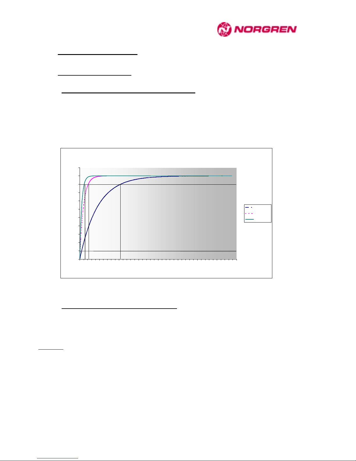
FD67 Profibus-DP Manual
78
8.3 Analogue I/O modules
8.3.1 Specific characteristics
8.3.1.1 Smoothing (Analogue input modules only)
The analogue signal can be prefiltered in the device, e.g. to reduce sensitivity to short-time measurement
variations.
Measurement time per channel is 2,0 ms. The total time of a cycle results from the measurement time per
channel + 2,5 ms. The graph below shows the module behav iour to the response time in an active
channel.
Response time on filtered active channel
0
0,1
0,2
0,3
0,4
0,5
0,6
0,7
0,8
0,9
1
1,1
0 250 500 750 1000 1250 1500 1750 2000
Time [ms]
Mesured size
Strong
Medium
Weak
♦ Fig. 8-1 : Time-dependent behaviour of smoothing in FD67 analogue input modules
8.3.1.2 Delta (Analogue input modules only)
This value sets the number of increments to increase or reduce the last measured value, in order to send
the analogue input value from the module to the bus node. This parameter can be used to reduce the bus
load of the internal system connection.
Example :
The last measured value was 1000. With a delta of 100, the next measured value will only be
sent, if it is < 900 or > 1100.
Page 84

FD67 Profibus-DP Manual
79
8.3.2 FD67AIVM120004
8.3.2.1 Identification
Compact module Part No. Process data ID
Input Output
Analogue input voltage M12 FD67AIVM120004 4 words - 42
hex
43
hex
DD
hex
7C
hex
8.3.2.2 I/O data
8.3.2.2.1 Input data IDM
Word 0 1 2 3
Byte 0 1 2 3 4 5 6 7
Measured
value
Channel 0 Channel 1 Channel 2 Channel 3
8.3.2.2.2 Byte sequence High/Low - Motorola (standard setting)
Byte Byte 0 (High-Byte) Byte 1 (Low-Byte)
Bit 15 14 13 12 11 10 9 8 7 6 5 4 3 2 1 0
Value VZ 2
14 213 212 211 210 29 28 27 26 25 24 23 22 21 20
8.3.2.2.3 Byte sequence Low/High - Intel
Byte Byte 0 (Low-Byte) Byte 1 (High-Byte)
Bit 15 14 13 12 11 10 9 8 7 6 5 4 3 2 1 0
Value 27 26 25 24 23 22 21 20 VZ 2
14 213 212 211 210 29 28
Page 85

FD67 Profibus-DP Manual
80
8.3.2.2.4 Representation of analogue values
Measured value
Area
Diagnosis Measuring range
0..10 V
binary hexadecimal decimal
>10 V 0111 1111 1111 1111 7FFF 32767 Overshooting yes
10 V
5V
0,305mV
0
0111 1111 1111 1111
0011 1111 1111 1111
0000 0000 0000 0001
0000 0000 0000 0000
7FFF
3FFF
0001
0000
32767
16383
1
0
Nominal range -
< 0V 0000 0000 0000 0000 0000 0 Undershooting -
Measured value Measuring range
+/-10 V
binary hexadecimal decimal
Area
Diagnosis
>10 V 0111 1111 1111 1111 7FFF 32767 Overshooting yes
10 V
5V
0,305mV
0
0111 1111 1111 1111
0011 1111 1111 1111
0000 0000 0000 0001
0000 0000 0000 0000
7FFF
3FFF
0001
0000
32767
16383
1
0
Nominal range -
-0,305mV
-5V
-10V
1111 1111 1111 1111
1100 0000 0000 0001
1000 0000 0000 0000
FFFF
C000
8000
-1
-16384
-32768
Nominal range -
< -10V 1000 0000 0000 0000 8000 -32768 Undershooting yes
8.3.2.3 Parameter bytes
Byte Signification
0 Settings channel 0
1 Reserved
2
3
Channel 0 : Delta
4 Settings channel 1
5 Reserved
6
7
Channel 1 : Delta
8 Settings channel 2
9 Reserved
10
11
Channel 2 : Delta
12 Settings channel 3
13 Reserved
14
15
Channel 3 : Delta
Page 86

FD67 Profibus-DP Manual
81
8.3.2.4 Bit assignments of parameter bytes
Bytes 0,4,8,12 Settings channels 0,1,2,3
7 6 5 4 3 2 1 0
Measuring range :
00 : inactive
01 : 0..10V
10 : +/- 10V
Diagnosis14
0 : report
1 : do not report
Data format :
0 : Byte sequence High/Low (Motorola)
1 : Byte sequence Low/High (Intel)
Smoothing :
00 : none
01 : weak
10 : moderate
11 : strong
Reserved
Bytes (2,3),(6,7),(10,11),(14,15) Channels (0,1,2,3) : Delta
Type of data Unsigned16
Admissible values 0..32767
Unused channels should be disabled to optimise cycle time.
14
Diagnostic information of the corresponding channel.
Page 87

FD67 Profibus-DP Manual
82
8.3.3 FD67AOVM120004
8.3.3.1
Identification
Compact module Part No. Process data ID
Input Output
Analogue output v oltage M12 FD67AOVM120004 - 4 words 82
hex
43
hex
DD
hex
86
hex
8.3.3.2 I/O data
8.3.3.2.1 Output data ODM
Word 0 1 2 3
Byte 0 1 2 3 4 5 6 7
Measured
value
Channel 0 Channel 1 Channel 2 Channel 3
8.3.3.2.2 Byte sequence High/Low - Motorola (standard setting)
Byte Byte 0 (High-Byte) Byte 1 (Low-Byte)
Bit 15 14 13 12 11 10 9 8 7 6 5 4 3 2 1 0
Value VZ -
-
-
- 2
10 29 28 27 26 25 24 23 22 21 20
8.3.3.2.3 Byte sequence Low/High - Intel
Byte Byte 0 (Low-Byte) Byte 1 (High-Byte)
Bit 15 14 13 12 11 10 9 8 7 6 5 4 3 2 1 0
Value 27 26 25 24 23 22 21 20 VZ
- - - - 2
10 29 28
Page 88

FD67 Profibus-DP Manual
83
8.3.3.2.4 Representation of analogue values
Measured value Output range
0..10 V
binary hexadecimal decimal
Area
10 V
5V
0,305mV
0
0000 0111 1111 1111
0000 0011 1111 1111
0000 0000 0000 0001
0000 0000 0000 0000
07FF
03FF
0001
0000
2047
1023
1
0
Nominal range
Measured value Output range
+/-10 V
binary hexadecimal decimal
Area
10 V
5V
0,305mV
0
0000 0111 1111 1111
0000 0011 1111 1111
0000 0000 0000 0001
0000 0000 0000 0000
07FF
03FF
0001
0000
2047
1023
1
0
Nominal range
-0,305mV
-5V
-10V
1xxx x111 1111 1111
1xxx x100 0000 0001
1xxx x000 0000 0001
FFFF
FC01
F800
-1
-1023
-2048
Nominal range
8.3.3.3 Parameter bytes
Byte Signification
0 Settings channel 0
1 Reserved
2 Reserved
3 Reserved
4 Settings channel 1
5 Reserved
6 Reserved
7 Reserved
8 Settings channel 2
9 Reserved
10 Reserved
11 Reserved
12 Settings channel 3
13 Reserved
14 Reserved
15 Reserved
Page 89

FD67 Profibus-DP Manual
84
8.3.3.4 Bit assignments of parameter bytes
Bytes 0,4,8,12 Settings channels 0,1,2,3
7 6 5 4 3 2 1 0
Output range :
00 : inactive
01 : 0..10V
10 : +/- 10V
Diagnosis15
0 : report
1 : do not report
Data format :
0 : Byte sequence High/Low (Motorola)
1 : Byte sequence Low/High (Intel)
Reserved
Unused channels should be disabled to optimise cycle time.
15
Diagnostic information of the corresponding channel.
Page 90

FD67 Profibus-DP Manual
85
8.3.4 FD67AOCM120004
8.3.4.1
Identification
Compact module Part. No Process data ID
Input Output
Analogue output current M12 FD67AOCM120004 - 4 words 82
hex
43
hex
DD
hex
90
hex
8.3.4.2 I/O data
8.3.4.2.1 Output data ODM
Word 0 1 2 3
Byte 0 1 2 3 4 5 6 7
Measured
value
Channel 0 Channel 1 Channel 2 Channel 3
8.3.4.2.2 Byte sequence High/Low - Motorola (standard setting)
Byte Byte 0 (High-Byte) Byte 1 (Low-Byte)
Bit 15 14 13 12 11 10 9 8 7 6 5 4 3 2 1 0
Value 0
- - - - 2
10 29 28 27 26 25 24 23 22 21 20
8.3.4.2.3 Byte sequence Low/High - Intel
Byte Byte 0 (Low-Byte) Byte 1 (High-Byte)
Bit 15 14 13 12 11 10 9 8 7 6 5 4 3 2 1 0
Value 27 26 25 24 23 22 21 20 0
- - - - 2
10 29 28
8.3.4.2.4 Representation of analogue values
Measured value Output range
0..20 mA
binary hexadecimal decimal
Area
20 mA
10 mA
4 mA
0 mA
0xxx x111 1111 1111
0xxx x011 1111 1111
0xxx x001 1001 1001
0xxx x000 0000 0000
07FF
03FF
0199
0000
2047
1023
409
0
Nominal range
Measured value Output range
4..20 mA
binary hexadecimal decimal
Area
20 mA
10 mA
4 mA
0xxx x111 1111 1111
0xxx x010 1111 1111
0xxx x000 0000 0000
07FF
02FF
0000
2047
767
0
Nominal range
Page 91

FD67 Profibus-DP Manual
86
8.3.4.3 Parameter bytes
Byte Signification
0 Settings channel 0
1 Reserved
2 Reserved
3 Reserved
4 Settings channel 1
5 Reserved
6 Reserved
7 Reserved
8 Settings channel 2
9 Reserved
10 Reserved
11 Reserved
12 Settings channel 3
13 Reserved
14 Reserved
15 Reserved
8.3.4.4 Bit assignments of parameter bytes
Bytes 0,4,8,12 Settings channels 0,1,2,3
7 6 5 4 3 2 1 0
Output range :
00 : inactive
01 : 4..20mA
10 : 0..20mA
Diagnosis16
0 : report
1 : do not report
Data format :
0 : Byte sequence High/Low (Motorola)
1 : Byte sequence Low/High (Intel)
Reserved
Unused channels should be disabled to optimise cycle time.
16
Diagnostic information of the corresponding channel.
Page 92

FD67 Profibus-DP Manual
87
8.3.5 FD67AICM120004
8.3.5.1 Identification
Compact module Part. No Process data ID
Input Output
Analogue input current M12 FD67AICM120004 4 words - 42
hex
43
hex
DD
hex
9A
hex
8.3.5.2 I/O data
8.3.5.2.1 Input data IDM
Word 0 1 2 3
Byte 0 1 2 3 4 5 6 7
Measured
value
Channel 0 Channel 1 Channel 2 Channel 3
8.3.5.2.2 Byte sequence High/Low - Motorola (standard setting)
Byte Byte 0 (High-Byte) Byte 1 (Low-Byte)
Bit 15 14 13 12 11 10 9 8 7 6 5 4 3 2 1 0
Value VZ 2
14 213 212 211 210 29 28 27 26 25 24 23 22 21 20
8.3.5.2.3 Byte sequence Low/High - Intel
Byte Byte 0 (Low-Byte) Byte 1 (High-Byte)
Bit 15 14 13 12 11 10 9 8 7 6 5 4 3 2 1 0
Value 27 26 25 24 23 22 21 20 VZ 2
14 213 212 211 210 29 28
8.3.5.2.4 Representation of analogue values
Measured value Measuring range
0..20 mA
binary hexadecimal decimal
Area Diagnosis
> 20 mA 0111 1111 1111 1111 7FFF 32767 Ov ershooting yes
20 mA
10 mA
4 mA
0
0111 1111 1111 1111
0011 1111 1111 1111
0001 1001 1001 1001
0000 0000 0000 0000
7FFF
3FFF
1999
0000
32767
16383
6553
0
Nominal range -
< 0 mA 0000 0000 0000 0000 0000 0 Undershooting -
Measured value Measuring range
4..20 mA
binary hexadecimal decimal
Area Diagnosis
>20 mA 0111 1111 1111 1111 7FFF 32767 Overshooting ja
20 mA
10 mA
4 mA
0111 1111 1111 1111
0010 1111 1111 1010
0000 0000 0000 0000
7FFF
2FFA
0000
32767
12282
0
Nominal range -
< 4 mA 0000 0000 0000 0000 0000 0 Undershooting yes17
17
„Line breakage“ < 2mA or „Lower threshold undershot“ < 4mA
Page 93

FD67 Profibus-DP Manual
88
8.3.5.3 Parameter bytes
Byte Signification
0 Settings channel 0
1 Reserved
2
3
Channel 0 : Delta
4 Settings channel 1
5 Reserved
6
7
Channel 1 : Delta
8 Settings channel 2
9 Reserved
10
11
Channel 2 : Delta
12 Settings channel 3
13 Reserved
14
15
Channel 3 : Delta
8.3.5.4 Bit assignments of parameter bytes
Bytes 0,4,8,12 Settings channels 0,1,2,3
7 6 5 4 3 2 1 0
Measuring range :
00 : inactive
01 : 4..20mA
10 : 0..20mA
Diagnosis18
0 : report
1 : do not report
Data format :
0 : Byte sequence High/Low (Motorola)
1 : Byte sequence Low/High (Intel)
Smoothing :
00 : none
01 : week
10 : moderate
11 : strong
Reserved
Bytes (2,3),(6,7),(10,11),(14,15) Channels (0,1,2,3) : Delta
Type of data Unsigned16
Admissible values 0..32767
Unused channels should be disabled to optimise cycle time.
18
Diagnostic information of the corresponding channel.
Page 94

FD67 Profibus-DP Manual
89
8.3.6 Part. No FD67DODSC0016
8.3.6.1
Identification
Expander
module
Part. No Process data ID
Input Output
Valve module FD67DODSC0016 - 2 bytes 82
hex
01
hex
DD
hex
4B
hex
8.3.6.2 Bit assignments of I/O data
8.3.6.2.1 Output data ODM
Byte 0 (channels 00 to 07 )
Bit 7 6 5 4 3 2 1 0
Channel 07 06 05 04 03 02 01 00
Byte 1 (channels 08 to 15 )
Bit 7 6 5 4 3 2 1 0
Channel 15 14 13 12 11 10 09 08
8.3.6.3 Parameter bytes
Byte Signification
4 Reserved
5 Reserved
6 Reserved
7 Reserved
Page 95

FD67 Profibus-DP Manual
90
9 Glossary
9.1 General information about the Profibus
Bus segment The electrical specification of the RS-485 interface limits the number of
users on an RS485 network to 32. If more than 32 Profibus users are to
be used, then the network must be subdivided into segments by using
repeaters.
DP Distributed Periphery. Profibus protocol for high-speed cyclical data
exchange.
Freeze Mode The Input data of the slave are "frozen“.
GAP factor The number of bus cycles after which a DP master searches for new
active subscribers for inclusion in the token ring. This factor can be
modified to optimize the speed of a DP network.
GAP range The address range in which an active user searches for a new active
user. This range is always between the own address and the address of
the next active user already in the Token Ring. The range from the
highest address up to 127 does not belong to the GAP range.
GSD The devices master file describes the technical features of a Profibus
product. This file is required to configure a Profibus system, and is
provided by the device's manufacturer.
ID number A 16-bit number which clearly identifies a Profibus product. It is a
reference to the GSD file. More than one device can have the same ID
number, provided that the numbers can be written to a common GSD file.
This number is allocated by Profibus Nutzerorganisation e.V (Profibus
user organization).
IEC 61158 Globally recognized standard for Profibus DP and FMS which
supersedes the international standard EN 50 170 Volume 2.
Master Class 1 The master which carries out user data transfers.
Master Class 2 Master for control/startup and configuration tasks.
Byte Term used in IEC 61158. Equivalent to 1 byte or 8 bits.
IDM Input Data Map
ODM Output Data Map
PNO
P
rofibus Nutzerorganisation e.V. (Profibus user organisation)
Repeater Coupling element for signal conditioning between Profibus segments.
PLC Programmable Logic Controller
Sync-Mode The output data of the Slave are "frozen“.
Page 96

FD67 Profibus-DP Manual
91
Token The activ e user (master) in possession of the token can carry out data
exchange with the slaves which it has parameterized and configured. On
completion of the data cycle, the active user passes the token to the next
active user.
9.2 FD67 specific
Sensor short-circuit Short-circuit or overload at Pin 1 of the M12 socket causes the self-
resetting fuse to blow. Each M12 socket is separately fused. A red LED
indicates the fault at the associated M12 socket. This fault is indicated via
the DP diagnosis. The sensor supply restarts automatically after the fault
is cleared. Please not the specific characteristics of analogue A/O
modules.
Actuator cut-off Short-circuit or overload at an output causes the output to be disabled.
This fault is indicated to the DP master via the DP diagnosis. A red LED
indicates the fault at the associated M12 socket. The output is not
automatically re-enabled. The output or the actuator supply voltage must
be disabled after eliminating the cause of the fault. This clears the short
circuit memory.
Actuator warning W hen an output is disabled, the presence of 24V at the associated Pin of
the M12 socket is detected. This is an indication of a "short-circuit" to
+24. A probable cause of this diagnosis is a faulty connection, i.e. a
sensor was connected to a channel parameterized as an output. A red
LED indicates the fault at the associated M12 socket. This fault is
indicated to the DP master via the DP diagnosis. This fault does not
affect activation of the output. It is not possible to detect an actuator
warning when the output is enabled.
Undervoltage The voltages of the sensor supply and actuator supply are metered
separately. W hen the voltage drops below 18 V DC, a fault is indicated to
the DP master v ia the DP diagnosis. When sensor supply undervoltage is
detected, the LED labeled "U
S
" is lit red. When actuator supply
undervoltage is detected, the LED labeled "U
A
" is lit red. This diagnosis
can be masked out via the parameterization.
No voltage This diagnosis is indicated to the DP master when the supply v oltage
drops below 12 V DC. This diagnosis can be masked out via the
parameterization.
External fault This diagnosis can only be generated by an input parameterized as a
diagnostic input. External fault is indicated when 0 V is present at this
input. Sensors/actuators which meet the DESINA specification are
supported. Alternately, the line can be monitored for open circuit by using
a diagnosis adapter.
Page 97

FD67 Profibus-DP Manual
92
10 Index of figures
♦
FIG. 3-1 : EXAMPLE OF A PROFIBUS NETWORK 6
♦
FIG. 4-1 : ASSEMBLING THE HOOD OF THE BUS NODE 9
♦
FIG. 4-2 : FE CONNECTION 10
♦
FIG. 4-3 : PIN ASSIGNMENTS OF THE 7/8“ POWER CONNECTOR 7/8“ (MINI-STYLE) 11
♦
FIG. 4-4 : ASSEMBLY OF THE 7/8“ POWER CONNECTOR (MINI-STYLE) 11
♦
FIG. 4-5 : CONTACT ASSIGNMENTS OF PROFIBUS M12 SOCKETS (B-ENCODED) 12
♦
FIG. 4-6 : ASSEMBLING OF THE PROFIBUS CABLE 12
♦
FIG. 5-1 : CONFIGURATION EXAMPLE 24
♦
FIG. 5-2 : HARDWARE-CONFIGURATOR IN A SIMATIC S7 ENVIRONMENT 25
♦
FIG. 6-1 : MOUNTING THE HOOD OF THE BUS NODE 29
♦
FIG. 6-2 : INTERCONNECTION OF SYSTEM COMPONENTS 30
♦
FIG. 7-1 : LED DISPLAYS ON THE BUS NODE 35
♦
FIG. 7-2 : LOCATION OF THE US AND UA DISPLAYS ON THE BUS NODE 36
♦
FIG. 7-3 : LOCATION OF THE US AND UA DISPLAYS,. ART.-NO 56 600 38
♦
FIG. 7-4 : LOCATION OF THE POWER DISTRIBUTOR DISPLAYS 42
♦
FIG. 7-5 : MAX. NUMBER OF CHANNEL-RELATED DIAGNOSIS 44
♦
FIG. 8-1 : TIME-DEPENDENT BEHAVIOUR OF SMOOTHING IN FD67 ANALOGUE INPUT
MODULES 78
Page 98

FD67 Profibus-DP Manual
93
11 Index of tables
♦
TABLE 3-1 : MAX. ADMISSIBLE CABLE LENGTHS IN A PROFIBUS SEGMENT 7
♦
TABLE 5-1 : PROFIBUS IDENTIFICATIONS OF I/O MODULES 17
♦
TABLE 7-1 : STATUS DISPLAYS OF THE BUSRUN LED ON THE BUS NODE 35
♦
TABLE 7-2 : STATUS DISPLAYS OF THE CFGF LED ON THE BUS NODE 35
♦
TABLE 7-3 : STATUS OF THE SYSTEM COMMUNICATION ON THE BUS NODE 36
♦
TABLE 7-4 : STATUS OF SENSOR AND SYSTEM SUPPLY ON THE BUS NODE 36
♦
TABLE 7-5 : STATUS OF THE ACTUATOR SUPPLY ON THE BUS NODE 37
♦
TABLE 7-6 : STATUS OF THE SYSTEM COMMUNICATION 38
♦
TABLE 7-7 : STATUS OF THE SENSOR AND SYSTEM SUPPLY (BUSIN DISPLAY) 38
♦
TABLE 7-8 : STATUS OF THE INTERNAL ACTUATOR SUPPLY (BUSIN DISPLAY) 39
♦
TABLE 7-9 : STATUS OF THE EXTERN POWER DISPLAYS (ART.-NO 56 600 ONLY) 39
♦
TABLE 7-10 : M12 SOCKETS – LED DIAGNOSIS DISPLAYS 39
♦
TABLE 7-11 : RELATIONSHIP BETWEEN SIGNAL-LOGICAL REPRESENTATION AND LED
RESPONSE - INPUT 40
♦
TABLE 7-12 : RELATIONSHIP BETWEEN SIGNAL-LOGICAL REPRESENTATION AND LED
RESPONSE - OUTPUT 40
♦
TABLE 7-13 : M12 SOCKETS – LED DIAGNOSIS DISPLAYS AI4 (U) / (I) 41
♦
TABLE 7-14 : M12 SOCKETS – LED DIAGNOSIS DISPLAYS AO4 (U) / (I) 41
♦
TABLE 7-15 : 6-PIN M12 SOCKETS – LED DISPLAYS 42
♦
TABLE 7-16 : TROUBLESHOOTING IN A PROFIBUS NETWORK 59
♦
TABLE 7-17 : MAX. ADMISSIBLE CABLE LENGHTS IN A PROFIBUS SEGMENT 59
♦
TABLE 7-18 : TROUBLESHOOTING IN THE INTERNAL SYSTEM CONNECTION 60
 Loading...