

Page 1

PAMS Technical Documentation
NSD–3 Series Transceivers
UI Module UE4
Issue 1 06/1999 Nokia Mobile Phones Ltd.
Page 2
NSD–3
UI Module UE4
PAMS Technical Documentation
CONTENTS
UI Module 4. . . . . . . . . . . . . . . . . . . . . . . . . . . . . . . . . . . . . . . . . . . . . .
Introduction 4. . . . . . . . . . . . . . . . . . . . . . . . . . . . . . . . . . . . . . . . . .
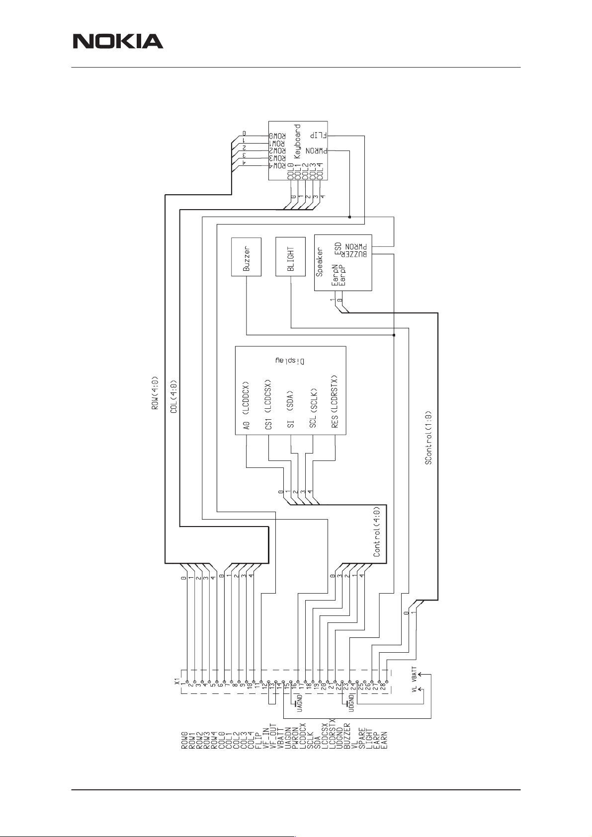
Baseband Block Diagram 5. . . . . . . . . . . . . . . . . . . . . . . . . . .
The Engine Interface 6. . . . . . . . . . . . . . . . . . . . . . . . . . . . . . .
The LCD Module Interface 8. . . . . . . . . . . . . . . . . . . . . . . . . .
Functional Description 9. . . . . . . . . . . . . . . . . . . . . . . . . . . . . . . .
Power Distribution Diagram 9. . . . . . . . . . . . . . . . . . . . . . . . . .
Display Circuit 9. . . . . . . . . . . . . . . . . . . . . . . . . . . . . . . . . . . . .
Keyboard 10. . . . . . . . . . . . . . . . . . . . . . . . . . . . . . . . . . . . . . . . .
Keyboard Matrix 11. . . . . . . . . . . . . . . . . . . . . . . . . . . . . . . . . . .
Power Key 11. . . . . . . . . . . . . . . . . . . . . . . . . . . . . . . . . . . . . . . .
Backlighting 12. . . . . . . . . . . . . . . . . . . . . . . . . . . . . . . . . . . . . . .
Display 13. . . . . . . . . . . . . . . . . . . . . . . . . . . . . . . . . . . . . . . . . . .
Keyboard 13. . . . . . . . . . . . . . . . . . . . . . . . . . . . . . . . . . . . . . . . .
Buzzer 13. . . . . . . . . . . . . . . . . . . . . . . . . . . . . . . . . . . . . . . . . . . .
Speaker 14. . . . . . . . . . . . . . . . . . . . . . . . . . . . . . . . . . . . . . . . . .
Parts list of UE4 (EDMS Issue 11.4) Code: 0200860 15. . . . . . . .
Schematic Diagrams A3 (at the back of the binder)
Block Diagram of UIF Module (Version 9.0 Edit 45) layout 11 B–1.
Circuit Diagram of Buzzer Module (Version 9.0 Edit 29) layout 11 B–2
Circuit Diagram of Speaker Module (Version 9.0 Edit 29) layout 11 B–2
Circuit Diagram of LCD Module (Version 9.0 Edit 21) layout 11 B–3
Circuit Diagram of Backlight (Version 9.0 Edit 25) layout 11 B–4. .
Circuit Diagram of Keyboard (Version 9.0 Edit 40) layout 11 B–5. .
Layout Diagram of UE4 – Top (Version 11) B–6. . . . . . . . . . . . . . . . .
Layout Diagram of UE4 – Bottom (Version 11) B–6. . . . . . . . . . . . . .
Page 2
Nokia Mobile Phones Ltd.
Issue 1 06/1999
Page 3
PAMS Technical Documentation
NSD–3
UI Module UE4
This page intentionally left blank.
Issue 1 06/1999
Nokia Mobile Phones Ltd.
Page 3
Page 4
NSD–3
UI Module UE4
UI Module
Introduction
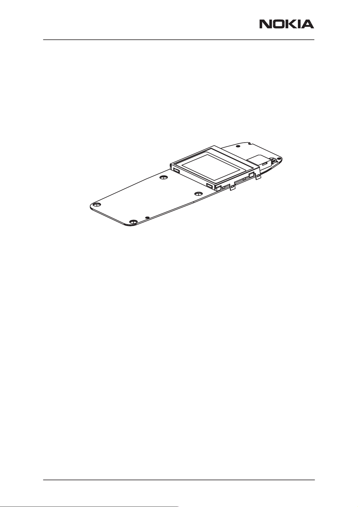
The UI module UE4 is a four layer PCB, which is connected to the system/RF PCB with a 28–pin spring connector.
PAMS Technical Documentation
Page 4
Nokia Mobile Phones Ltd.
Issue 1 06/1999
Page 5
PAMS Technical Documentation
Baseband Block Diagram
NSD–3
UI Module UE4
Issue 1 06/1999
Nokia Mobile Phones Ltd.
Page 5
Page 6

NSD–3
UI Module UE4
The Engine Interface
PAMS Technical Documentation
Pin Line Sym-
bol
1 ROW0 Keyboard matrix row 0 0 0.3xVBB V Low
2 ROW1 Keyboard matrix row 1 0 0.3xVBB V Low
3 ROW2 Keyboard matrix row 2 0 0.3xVBB V Low
4 ROW3 Keyboard matrix row 3 0 0.3xVBB V Low
5 ROW4 Keyboard matrix row 4 0 0.3xVBB V Low
6 COL0 Keyboard matrix column 0,
used for flip identification
7 COL1 Keyboard matrix column 1 0 0.3xVBB V Low
8 COL2 Keyboard matrix column 2 0 0.3xVBB V Low
Parameter Min Typ Max Unit Notes
0.7xVBB VBB High
0.7xVBB VBB High
0.7xVBB VBB High
0.7xVBB VBB High
0.7xVBB VBB High
0 0.3xVBB V Flip Open
0.7xVBB VBB Flip Closed
0.7xVBB VBB High
0.7xVBB VBB High
9 COL3 Keyboard matrix column 3 0 0.3xVBB V Low
0.7xVBB VBB High
10 COL4 Keyboard matrix column 4 0 0.3xVBB V Low
0.7xVBB VBB High
11 Signal1 Flip interrupt, not used 0 0.3xVBB V
0.7xVBB VBB
12 VF_IN Flash in 4.8 5.0 5.2 V Connected #13
13 VF_OUT Flash out 4.8 5.0 5.2 V Connected #12
14 VBATT Battery voltage 3.0 5.1 V
60 75 100 mA For lights
110 300 mA For buzzer
15
UAGND*
16 PWRON Power on key 0 0.3xVBB V Low / Power on
17 LCDCDX LCD driver code/data selection 0 0.3xVBB V Low
Analog ground 0 V
0.7xVBB VBB High
0.7xVBB VBB High
18 SCLK LCD driver serial clock 0 0.3xVBB V Low
0.7xVBB VBB High
0 4.0 MH
z
Page 6
Nokia Mobile Phones Ltd.
Issue 1 06/1999
Page 7

PAMS Technical Documentation
NSD–3
UI Module UE4
Pin
bol
19 SDA LCD driver serial data 0 0.3xVBB V Low
0.7xVBB VBB High
20 LCDCSX LCD driver chip select 0 0.3xVBB V Low / Active
0.7xVBB VBB High
21 LCDRSTX LCD driver reset 0 0.3xVBB V Low / Active
0.7xVBB VBB High
22
UDGND*
23 BUZZER Buzzer PWM control 0 2.85 V
24 VL Supply voltage 2.7 2.8 2.85 V
25 SPARE 0 0.3xVBB V Not used in UI
26 LIGHT Illumination control 0 0.3xVBB V Low
27 EARN Speaker neutral 0 1.78 Vpp
28 EARP Speaker positive 0 1.78 Vpp
Digital ground 0 V
300 uA
0.7xVBB VBB
0.7xVBB VBB High / Active
NotesUnitMaxTypMinParameterLine Sym-
* Ground position is on connector NOT BATTERY.
LCD
2815
114
UIM connector pads viewed from the GND side
Issue 1 06/1999
Nokia Mobile Phones Ltd.
Page 7
Page 8

NSD–3
UI Module UE4
The LCD Module Interface
PAMS Technical Documentation
Pin Line
Symbol
1 VL Supply voltage 2.7 2.8 2.85 V
2 SCLK Serial clock input 0 4.0 MHz VBB = 2.7V
3 SDA Serial data input 0 0.3xVBB
4 LCDCDX Control/display data flag input 0 0.3xVBB Control
5 LCDCSX Chip select input 0 0.3xVBB Active
6 OSC** External clock for LCD 30.4 32.0 33.6 kHz Connected to
7 UDGND* Ground 0 V
8 VOUT DC/DC voltage converter output 9
9 LCDRSTX Reset 0 0.3xVBB Active
Parameter Mini-
mum
0 VBB V
0.7xVBB VBB
0.7xVBB VBB Data
0.7xVBB VBB
0.7xVBB VBB
Typical
/ Nomi-
nal
Maxi-
mum
300 uA
Unit Notes
VBB on UI
* Ground position is on connector NOT BATTERY.
** External oscillator is not used in UE4.
19
Display Driver
Viewing trought LCD cell
LCD Module Interface
Page 8
Nokia Mobile Phones Ltd.
Issue 1 06/1999
Page 9

PAMS Technical Documentation
Functional Description
Power Distribution Diagram
PWRXON
VBB
VBATT
NSD–3
UI Module UE4
Buzzer
UAGND
UDGND
Display Circuit
The display circuit includes LCD module GD40 and two capacitors. The
LCD module is COG (Chip on Glass) technology. The connection method
for chip on the glass is ACF, Adhesive Conductive Film. The LCD module
is connected to UI board with gold wired elastomer. Capacitors are placed
on UI PCB.
The display driver includes hw–reset, voltage tripler or quadrupler which
depends on temperature, temperature compensating circuit and low power control. Driver includes 84x48 RAM memory which is used when some
elements are create on display. Elements can be create with software.
Driver doesn’t include CG–ROM. One bit in RAM is same as one pixel on
display.
LEDs of
Display
LEDs of
Keybord
Display
PWR
key
Issue 1 06/1999
Nokia Mobile Phones Ltd.
Page 9
Page 10

NSD–3
UI Module UE4
Keyboard
AGND
PAMS Technical Documentation
Typical value for node is marked with black when circuit is not active
Typical value for node is marked with gray when circuit is active
[4V]
[2.8V]
Page 10
Nokia Mobile Phones Ltd.
Issue 1 06/1999
Page 11

PAMS Technical Documentation
UI Module UE4
Keyboard Matrix
ROW/COL 0 1 2 3 4
0 FLIP Side Key Send End/Mode Side Key
1 NC Soft left Up Down Soft Right
2 NC 1 4 7 *
3 NC 2 5 8 0
4 PWR switch 3 6 9 #
NC = Not Connected
NSD–3
Power Key
Micro switch is used as a power key on UI module. Circuitry includes micro switch and two diodes which is needed for MAD interface. Power key
is connected to CCONT. Power switch is active in LOW state. The power
key circuit can be seen from the Display Circuit diagram on page 8.The
power key is connected to ROW4.
Up
Down
S RightS Left
EndSend
12 3
4
7
*
56
8
0
9
#
Issue 1 06/1999
Nokia Mobile Phones Ltd.
Page 11
Page 12

NSD–3
UI Module UE4
Backlighting
PAMS Technical Documentation
[4V]
[4V]
[2.6V]
[2.0V]
[0V]
[1.9V]
[2.6V]
[0V]
[1.2V]
[1.4V]
[0V]
[0V]
[0.7V]
[0.5V]
Page 12
Typical value for node is marked with black when circuit is not active
Typical value for node is marked with gray when circuit is active
Nokia Mobile Phones Ltd.
Issue 1 06/1999
Page 13

PAMS Technical Documentation
Display
Backlighting is provided by LEDs, three LED on right and three on left
side of display. LEDs are compatible with CL270–YG and those are side
illuminating. Light is on when LIGHT–signal is in HIGH state.
Color of LED is for
NSD–3
UI Module UE4
Pin Line
Symbol
14 VBAT Battery voltage 3.0 5.1 V Same supply for
Parameter Mini-
mum
43.4 51.4 59.6 mA LEDs
Typical
/ Nomi-
nal
Maxi-
mum
Unit Notes
Buzzer & Keyboard
Keyboard
In keyboard backlighting is made by 6 LEDs. LEDs are compatible with
CL190–YG. Backlighting is on when LIGHT–signal is on HIGH state.
Color of LED is for
– Keyboard : yellow–green, λ = 570nm
Pin Line
Symbol
14 VBAT Battery voltage 3.0 5.1 V Same supply for
Parameter Mini-
mum
55.3 62.4 69.9 mA LEDs
Typical
/ Nomi-
nal
Maxi-
mum
Unit Notes
Buzzer & Display
Buzzer
Buzzer for DCT3 generation phone is SMD type.
Typical value for node is marked with black when circuit is not active
Typical value for node is marked with gray when circuit is active
[0V]
[4V]
[4V]
[4V]
[0V]
Issue 1 06/1999
Nokia Mobile Phones Ltd.
Page 13
Page 14

NSD–3
UI Module UE4
Speaker
The speaker is sealed to A–cover and UI PCB with silicon gasket. With
that the frequency response is more constant. Speaker needs 6pcs of
1.2mm holes under component for leaking sound pressure into RF–section through UI module and 7pcs of 0.9mm holes left corner of UIM to
leak from RF–section back to up cavity of phone. RF–section between UI
module and engine acts like sound cage which is known. This gives better sound quality for the phone and it can be estimated in several environments.
Silicon gasket and speaker itself acts like water proofing elements in that
area. Water can come in speaker space between speaker and A–cover
but not further from there into the phone. On A–cover is 3pcs of leaking
holes which are not located top of the speaker. This holes gives better
sound quality and less sensitive for how well phone is pressed against of
head.
PAMS Technical Documentation
Speaker Circuit
[1.4V]
[1.4V]
Typical value for node is marked with black when circuit is not active
Typical value for node is marked with gray when circuit is active
Page 14
Nokia Mobile Phones Ltd.
Issue 1 06/1999
Page 15

NSD–3
PAMS Technical Documentation
UI Module UE4
Parts list of UE4 (EDMS Issue 11.4) Code: 0200860
ITEM CODE DESCRIPTION VALUE TYPE
R001 1430043 Chip resistor 2.2 k 5 % 0.063 W 0603
R002 1430155 Chip resistor 15 5 % 0.063 W 0603
R004 1430047 Chip resistor 3.3 k 5 % 0.063 W 0603
R006 1430043 Chip resistor 2.2 k 5 % 0.063 W 0603
R007 1430043 Chip resistor 2.2 k 5 % 0.063 W 0603
R008 1430155 Chip resistor 15 5 % 0.063 W 0603
R009 1430167 Chip resistor 47 5 % 0.063 W 0603
R010 1430087 Chip resistor 100 k 5 % 0.063 W 0603
R011 1825009 Varistor network 4xvwm18v 1206 1206
R014 1430035 Chip resistor 1.0 k 5 % 0.063 W 0603
R015 1430087 Chip resistor 100 k 5 % 0.063 W 0603
R016 1430159 Chip resistor 22 5 % 0.063 W 0603
R017 1430159 Chip resistor 22 5 % 0.063 W 0603
R019 1430122 Chip resistor 4.7 M 5 % 0.063 W 0603
C001 2320043 Ceramic cap. 22 p 5 % 50 V 0603
C002 2320043 Ceramic cap. 22 p 5 % 50 V 0603
C003 2320043 Ceramic cap. 22 p 5 % 50 V 0603
C004 2310784 Ceramic cap. 100 n 10 % 25 V 0805
C009 2310784 Ceramic cap. 100 n 10 % 25 V 0805
B001 5140087 Buzzer 85db 2600hz 3.6v 10x10x3. 10x10x3.5
Z001 3640035 Filt z>450r/100m 0r7max 0.2a 0603 0603
Z002 3640035 Filt z>450r/100m 0r7max 0.2a 0603 0603
H001 0200921 Gd40 lcd module
V001 4864388 Led Green 0603
V002 4864388 Led Green 0603
V003 4864388 Led Green 0603
V004 4860005 Led Green 0603
V005 4860005 Led Green 0603
V009 4864388 Led Green 0603
V010 4864388 Led Green 0603
V012 4864388 Led Green 0603
V013 4200836 Transistor BCX19 npn 50V 0.5A SOT23
V017 4860005 Led Green 0603
V020 4860005 Led Green 0603
V021 4860005 Led Green 0603
V022 4860005 Led Green 0603
V023 4200836 Transistor BCX19 npn 50V 0.5A SOT23
V025 4210100 Transistor BC848W npn 30 V SOT323
V026 4200875 Transistor BCX54–16 npn 45V 1.5A SOT89
V027 4100278 Diode x 2 BAV70 70V200mA COM
CAT.SOT23
V028 4100278 Diode x 2 BAV70 70 V 200 mA COM
CAT.SOT23
S001 5200120 Push button switch 6.4x5.2 smd
9850046 PCB UE4 118.0X41.5X0.8 M4 4/PA
Issue 1 06/1999
Nokia Mobile Phones Ltd.
Page 15
Page 16

NSD–3
UI Module UE4
PAMS Technical Documentation
This page intentionally left blank.
Page 16
Nokia Mobile Phones Ltd.
Issue 1 06/1999
 Loading...