

Page 1

PAMS Technical Documentation
THF–13 Series Transceivers
Troubleshooting
Instructions
Issue 1 08/99 Nokia Mobile Phones Ltd.
Page 2
THF–13
Troubleshooting Instructions
AMENDMENT RECORD SHEET
PAMS Technical Documentation
Amendment
Number
Date Inserted By Comments
08/99 OJuntune Issue 1
Page 2
Nokia Mobile Phones Ltd.
Issue 1 08/99
Page 3

PAMS Technical Documentation
Troubleshooting Instructions
CONTENTS
Troubleshooting Instructions 3. . . . . . . . . . . . . . . . . . . . . . . . . . . . . .
Equipment Setup For Tuning A Phone
With Covers Removed 4. . . . . . . . . . . . . . . . . . . . . . . . . . . . . . . . .
Phone is totally dead 5. . . . . . . . . . . . . . . . . . . . . . . . . . . . . . . . . .
Flash programming doesn’t work 6. . . . . . . . . . . . . . . . . . . . . . .
Flash Programming (1) 7. . . . . . . . . . . . . . . . . . . . . . . . . . . . .
Flash Programming failure (2) 8. . . . . . . . . . . . . . . . . . . . . . .
Power doesn’t stay on, or phone is jammed 9. . . . . . . . . . . . . .
Audio fault 10. . . . . . . . . . . . . . . . . . . . . . . . . . . . . . . . . . . . . . . .
Charger fault 11. . . . . . . . . . . . . . . . . . . . . . . . . . . . . . . . . . . . . .
Receiver Fault 12. . . . . . . . . . . . . . . . . . . . . . . . . . . . . . . . . . . . . . . . . .
THF–13
Page No
Transmitter fault 13. . . . . . . . . . . . . . . . . . . . . . . . . . . . . . . . . . . . . . . .
Issue 1 08/99
Nokia Mobile Phones Ltd.
Page 3
Page 4

THF–13
Troubleshooting Instructions
Troubleshooting Instructions
The following hints should facility finding the cause of the problem when
the circuitry seems to be faulty. This trouble shooting instruction is divided following section.
1. Phone is totally dead
2. Flash programming doesn‘t work
3. Power doesn‘t stay on or the phone is jammed
4. Audio fault.
5. Charging fault
6. Receiver fault
7. Transmitter fault
The first thing to do is carry out a through visual check of the module. En-
sure in particular that:
a) there are not any mechanical damages
b) soldered joints are OK
PAMS Technical Documentation
Page 4
Nokia Mobile Phones Ltd.
Issue 1 08/99
Page 5
PAMS Technical Documentation
Troubleshooting Instructions
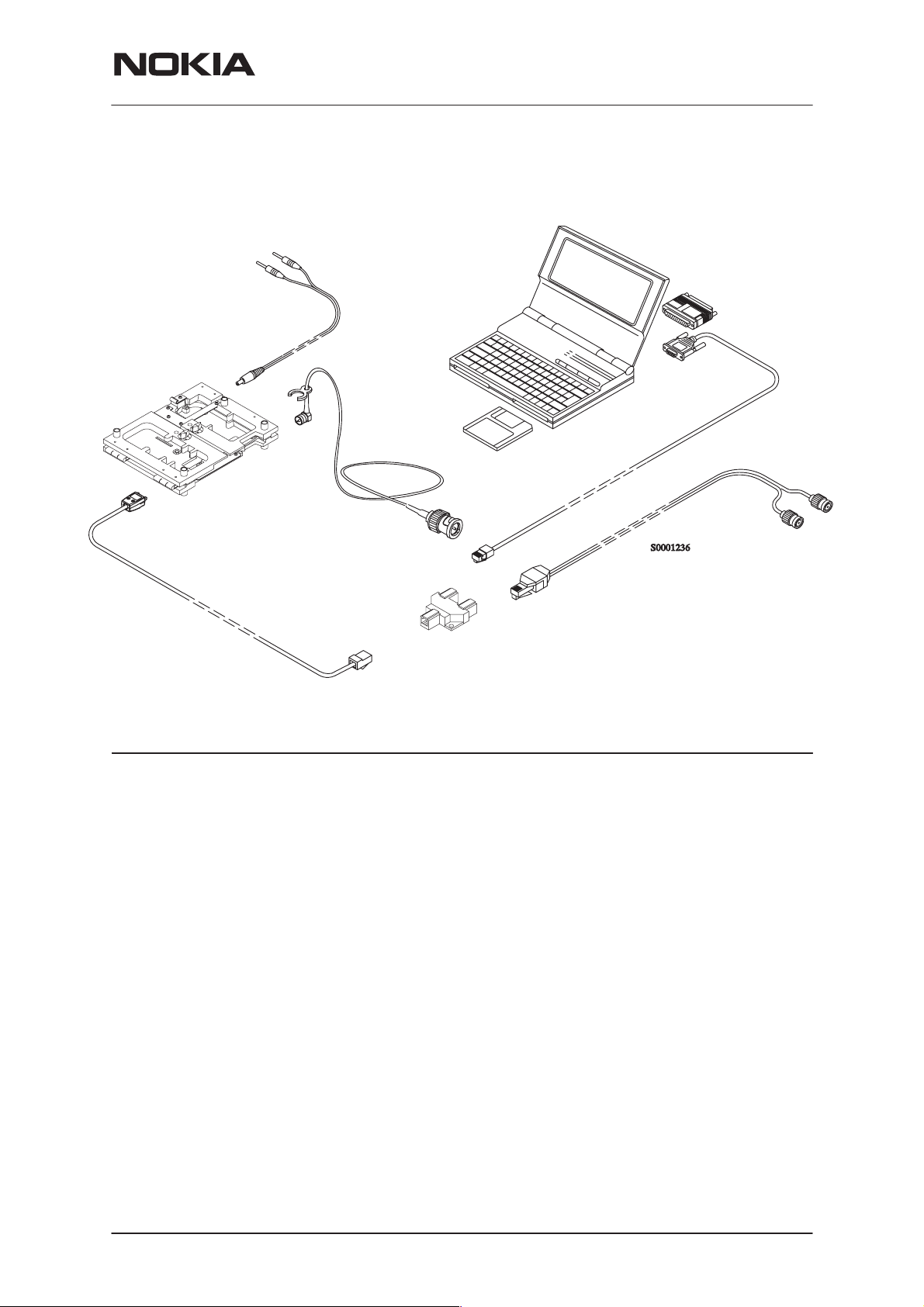
Equipment Setup For Tuning A Phone With Covers Removed
+4.1 V
8.
3.
9.
THF–13
1.
3.6V
5.
Item: Service accessory: Type Code:
1 Test frame * JBS–24 0770167
2 Modular T-Connector 4626134
3 DC Cable PCS–1 0730012
4 Antenna Cable XRC–1B 0730128
5 Service Cable SCH-5 0730098
6 Service MBUS Cable DAU–9S 0730108
7 Audio Cable ADS-1 0730011
8 Software protection key PKD-1 0750018
9 Service Software diskette 3.5” 0774112
WinTesla Service application 0774046
4.
6.
7.
2.
*) The nominal operating voltage for the JBS is 3.6 V.
Issue 1 08/99
Nokia Mobile Phones Ltd.
Page 5
Page 6

THF–13
Troubleshooting Instructions
Phone is totally dead
This means that phone doesn’t take current at all when the power switch
is pressed or when the watchdog disable is grounded R120.
Used battery voltage must be higher than 3.0 V. Otherwise the hardware
of PSA (N101) prevents totally to switch power on.
Phone is totally dead
YES
PAMS Technical Documentation
Check VBAT at PSA
(N101 pins 3,11,...) =3.6V
YES
N101 pin 13 (VL) 2.8 V
N101 pin 17 (VA) 2.8 V
when PWR switch is pressed
or watchdog disable pin is grounded
YES
See section: Power Doesn’t Stay On
NO Failure in VBAT line
Check F102
NO
PSA (N101) pin 22 0V when
PWR switch is pressed
YES
Faulty circuit N101
NO
Check PWR key
circuitry
Page 6
Nokia Mobile Phones Ltd.
Issue 1 08/99
Page 7

PAMS Technical Documentation
Flash programming doesn’t work
The fault finding diagrams for flash programming via system connector
are shown in the next figures.
There is regulator N230 which is used to produce the programming voltage (VPROG) it’s controlled by MCU and the same control line disables
watchdog.
In flash programming error cases the flash prommer can give some information about a fault.
The fault information messages could be:
– MCU doesn’t boot
– Serial clock line failure
– Serial data line failure
– External RAM fault
– Algorithm file or alias ID don’t find
– MCU flash Vpp error
THF–13
Troubleshooting Instructions
In cases that the flash programming doesn’t succeed there is a possibility
to check short circuits between the memories and the MCU.
This test is useful to do, when the fault information is: MCU doesn’t boot,
Serial clock line failure or Serial data line failure.
Issue 1 08/99
Nokia Mobile Phones Ltd.
Page 7
Page 8

THF–13
Troubleshooting Instructions
Flash Programming (1)
Flash programming doesn’t work
If the fault information from the prommer is:
YES
a) MCU doesn’t boot
b) serial data line failure
c) serial clock line failure
connect:
OK
PAMS Technical Documentation
Check MASI crystal
oscillator circuitry
PSA (N101) pin 13 (VL) 2.8V
PSA (N101) pin 17 (VA) 2.8V
YES
J121 (Purx)=”1” (2.8V)
YES
NO
Check that following lines are correct from X131 to D201
There could be open pins in circuits D200 (D211, D240)
MASI (N701) pin 62 14.74Mhz
clock signal: 2Vpp min.
YES
MBUS: X13 pin 11 ––> D201 pin 91
FBUS_TX: X131 pin13 –> D201 pin 89
FBUS_RX: X131 pin12 –> D201 pin 90
check also pullup and pulldown resistors
GND : X131 pin 9 –> GND
OK
If not, the PCB or D201,D221 are faulty
NO
NO Faulty circuit N100
See section: Phone is totally dead
or over loaded PurX line
Page 8
Nokia Mobile Phones Ltd.
Issue 1 08/99
Page 9

PAMS Technical Documentation
Flash Programming failure (2)
Flash progrmming doesn’t work
YES
If the fault information from the prommer is:
External RAM fault
YES
THF–13
Troubleshooting Instructions
Check pins of SRAM (D221)
Check control lines of SRAM:
CS1,_WE,__OE...
Flash progrmming doesn’t work
YES
If the fault information from the prommer is:
MCU flash Vpp error
YES
D210 pin13 (C211)
Vpp=2.8V
YES
NO
Check output of regulator
N230 pin 4 Vpp=2.8V
YES
Flash progrmming doesn’t work
YES
If the fault information from the prommer is:
Algorithm file or alias ID don’t find, ID is unknown etc.
YES
Check pins of FLASH (D210)
Check control lines and data/address lines
of FLASH: _CP,_OE_WE...
NO
Check control line to
regulator
YES
NO
Faulty
component
N201
Faulty component
D210
Issue 1 08/99
Check PCB
Regulator faulty
Nokia Mobile Phones Ltd.
Page 9
Page 10

THF–13
Troubleshooting Instructions
PAMS Technical Documentation
Power doesn’t stay on, or phone is jammed
If this kind of fault has come after flash programming, there are most
probably open pins in ICs.
The soldered joints of ICs: D201 (MCU), D210 (FLASH), N101 (PSA),
D221 (SRAM) are useful to check at first.
Normally the power will be switched of by PSA (N101) after 10 seconds, if
the watchdog of the PSA can not be served by software.
The watchdog updating can be seen by oscilloscope at pin 23 (POWEROFFX) of PSA.
In normal case there is a short pulse from ”1” –> 0 every now and then
depending on what the software is doing.
The power off function of PSA can be prevented by connecting a short
circuit wire from PSA pin 24 to ground, note that flash programming voltage goes on also.
Check crystal
oscillator circuitry
Power doesn’t stay on or phone is jammed
YES
PSA watchdog is served?
(pin 23 pulses 1 –> 0)
NO
Connect watchdog disable line to GND (R210)
OK
PSA (N101) pin 13 (VL) 2.8V
PSA (N101) pin 17 (VA) 2.8V
YES
N101 pin 16 PURX = ”1” 2.8V
YES
NO
MASI (701)pin 62 14.74MHz
clock signal: 2Vpp min.
YES
software is able to run
YES
NO
NO Faulty circuit N101
check UI module
If power is switched off
after few seconds, check
BSI and BTEMP lines
VBAT is correct
3.6 V
or over loaded PurX line
YES
N101 is faulty
Page 10
Open pins or faulty circuit:
D201, D210, D221, N101
Nokia Mobile Phones Ltd.
Issue 1 08/99
Page 11

PAMS Technical Documentation
Audio fault
MICROPHONE LEVEL / MODULATION LEVEL FAULT
THF–13
Troubleshooting Instructions
TXBPO COMI
MIC
EXTMIC
IF
PIN 45
SCR
245mVrms
DESCR
COMPR
RXAGC
PREEM AGC LIM
TXTRI+TXPOST
HF CONTROL
EARSFIL VOL
RXATT
TXLP
WTRFIL+WPOSFIL
SUM
EARPOST
VarFilter
EARAMP
MICAM
Signal levels are measured by oscilloscope and input signal frequency is 1 kHz, deviation 3kHz and generator voltage level 260mV.
RXTRI
TXMUX1
EXTMIC
EARPHONE LEVEL / MODULATION LEVEL FAULT
RXAAF EXPCOMP
MICTRI
PIN 43 PIN 44
RXMUX+AAFIL
TXMUX2
258mVrms 248mVrms
DEEMP
TXAAF
TXBPO
COMI
TXATT
PIN 46
MOD
304mVrms
EARP
EARN
EXTEAR
VOLI
FILO EXPI
FILO
EXPI
EXPO
VOLI
Signal levels are measured by oscilloscope and received signal audio frequency is 1 kHz, deviation 3kHz and power level –53dBm.
Issue 1 08/99
Nokia Mobile Phones Ltd.
EXPO
PIN 27
PIN 28
PIN 29
PIN 30
140mVrms
140mVrms
168mVrms
100mVrms
EARP
EXTEARPIN 26IF 124rVrms
PIN 33
PIN 35
43mVrms
43mVrms
Page 11
Page 12

THF–13
Troubleshooting Instructions
Charger fault
Nothing happens when charger is connected
PAMS Technical Documentation
YES
Voltage level at pin 8 of PSA (N101)
is higher than 0.4 V when charger is connected
YES
Check N101
Display Information: Not charging
YES
Voltage level at pin 100 of MCU (D201)
is about 0.8 V (BSI –resistor 39K) when
power is connected
Depends about BSI resistor value
Voltage level at pin 99 of MCU (D201)
is about 0.5 V when power is connected
BTEMP resistor value should be 47 k
32 Hz square wave frequency at pin 7 of CHAPS (N100)
YES
YES
YES
NO
Check
X131, F150, L150
R182,R1 13,R111,R
105
NO Check
X131,R206,R215
NO
NO
Check
X131,R203,R202
Check
N101
Voltage levels at pins 5 and 12 of CHAPS (N100)
are same as VBAT
YES
Voltage levels at pins 5 and 12 of CHAPS (N100)
rises when charger is connected
NO
NO
Check
R102, N100
Check
N100
Page 12
Nokia Mobile Phones Ltd.
Issue 1 08/99
Page 13

PAMS Technical Documentation
Receiver Fault
THF–13
Troubleshooting Instructions
Receiver fault
Simplex sens.
(TX off)
OK
TX spectrum
OK
Check duplex
filter Z640
FAIL
FAIL
See earphone level fault
OK
IF signal OK
after R381
Transmitter
fault
RX–VCO
oscillating
OK
FAIL
FAIL
Check G420
VRX, VPLL
OK?
OK
RXINJ
OK at V350
collector
FAIL
Check R341, R360–
R363, C360–C363,
V360, L361
OK
FAIL
OK
Check N101 (PSA)
1. IF
at N370/16
OK?
FAIL
RF level
in Z330
input
OK
RF level
in Z340
output
FAIL
OK
Check N370, C370–382,
R373
,R374&R381 & Z370
FAIL
Check R301–R314
C301 – C314
R320–R325
V310 & V320
L301 – l311
Issue 1 08/99
FAIL
VCO–freq
OK
Check: RXINJ level at V350
base and components R350–356
& C350–C354 & V350
Nokia Mobile Phones Ltd.
Check voltage doubler voltage at N400 pin 18
Check R420–R425, C420–427,
N400 & G410
NOTE!!! ”Check” means the checking of
component values, connections, voltages,
signal levels etc. if components does not
work, it has to be changed
Check Z330–Z340,
Z330–Z341, R340–R341
V330
Page 13
Page 14

THF–13
Troubleshooting Instructions
Transmitter fault
Check doubler voltage at C406 (5–5.3V), VPLL (2.8V),
Transmitter fault
VTX (2.8V). Check VCTCXO voltage and frequency
(14.85 MHz). Check SCLK, SDAT and SLE –lines
PAMS Technical Documentation
FAIL
Transmitter
frequency
OK
OK
Power OK after
tuning
FAIL
Vpc N611/8
1.5V – 2.4V (high level)
OK
Vreg N611/1
2.7V – 2.9V
OK
FAIL
OK
FAIL
Check: L621, R622, TXE
V611, V631, V632, V630
V634, R641, C646, R631
R632, R633
1W<Pout<1.6W at
C664. Disconnect the
C664 during measu–
rements
TX–VCO
freq and spectrum
OK (TXE OFF)
OK
OK
Check Z640 TX–pin
soldering. If OK replace
OK
Z640
Buffer V440
output freq. and
spectrum OK
(TXE OFF)
OK
N611 freq
and spectrum OK
when duplex filt.
not connected
FAIL
Check: C662, C663, C664
C666. If ok
replace N611
FAIL
OK
Check: V440 operating
voltage and bias.
Check soldering of duplex
filter V640 If ok replace
filter.
FAIL
Check: L623. If not OK
Replace N101 or N701
Replace G430
Page 14
FAIL
FAIL
Check L652, L654, C658
TXINJ level
7–9 dBm
FAIL
VCO output
–1..+2dBm
OK
C659, C660. If ok,
replace Z611.
Check operating voltage
OK
and bias of V440. Check
C440, R442,C604. If OK
replace V440.
Nokia Mobile Phones Ltd.
Issue 1 08/99
 Loading...