

Page 1

PAMS Technical Documentation
THF-13 Series Transceivers
General Information
Issue 1 08/99 Nokia Mobile Phones Ltd.
Page 2

THF-13
General Information
PAMS Technical Documentation
AMENDMENT RECORD SHEET
Amendment
Number
Date Inserted By Comments
08/99 OJuntune Issue 1
Page 2
Nokia Mobile Phones Ltd.
Issue 1 08/99
Page 3

PAMS Technical Documentation
CONTENTS
Product Selection 1 – 4. . . . . . . . . . . . . . . . . . . . . . . . . . . . . . . . . . . . . . .
Handportable 1 – 4. . . . . . . . . . . . . . . . . . . . . . . . . . . . . . . . . . . . . . . .
Desktop Option 1 – 5. . . . . . . . . . . . . . . . . . . . . . . . . . . . . . . . . . . . . .
Basic Car Kit (CARK–64) Option 1 – 6. . . . . . . . . . . . . . . . . . . . . . .
Advanced Hands Free Car Installation (CARK–91) Option 1 – 7.
Module and Product Lists 1 – 8. . . . . . . . . . . . . . . . . . . . . . . . . . . . . . . .
Technical Specifications 1 – 9. . . . . . . . . . . . . . . . . . . . . . . . . . . . . . . . .
General Specifications of Transceiver THF–13 1 – 9. . . . . . . . . . .
Modes of Operation 1 – 9. . . . . . . . . . . . . . . . . . . . . . . . . . . . . . . .
Maximum ratings 1 – 10. . . . . . . . . . . . . . . . . . . . . . . . . . . . . . . . . . .
DC Characteristics 1 – 10. . . . . . . . . . . . . . . . . . . . . . . . . . . . . . . . .
AC Characteristics 1 – 10. . . . . . . . . . . . . . . . . . . . . . . . . . . . . . . . .
External Connections 1 – 13. . . . . . . . . . . . . . . . . . . . . . . . . . . . . . .
System connector 1 – 14. . . . . . . . . . . . . . . . . . . . . . . . . . . . . . . . . .
Battery connector 1 – 17. . . . . . . . . . . . . . . . . . . . . . . . . . . . . . . .
Functional Description 1 – 18. . . . . . . . . . . . . . . . . . . . . . . . . . . . . . . .
Circuit Description 1 – 18. . . . . . . . . . . . . . . . . . . . . . . . . . . . . . . . . .
Block Diagram 1 – 18. . . . . . . . . . . . . . . . . . . . . . . . . . . . . . . . . . . . .
Interconnection Diagram 1 – 19. . . . . . . . . . . . . . . . . . . . . . . . . . . . . .
Power Distribution Diagram 1 – 20. . . . . . . . . . . . . . . . . . . . . . . . . .
THF-13
General Information
Page No
Issue 1 08/99
Nokia Mobile Phones Ltd.
Page 3
Page 4
THF-13
General Information
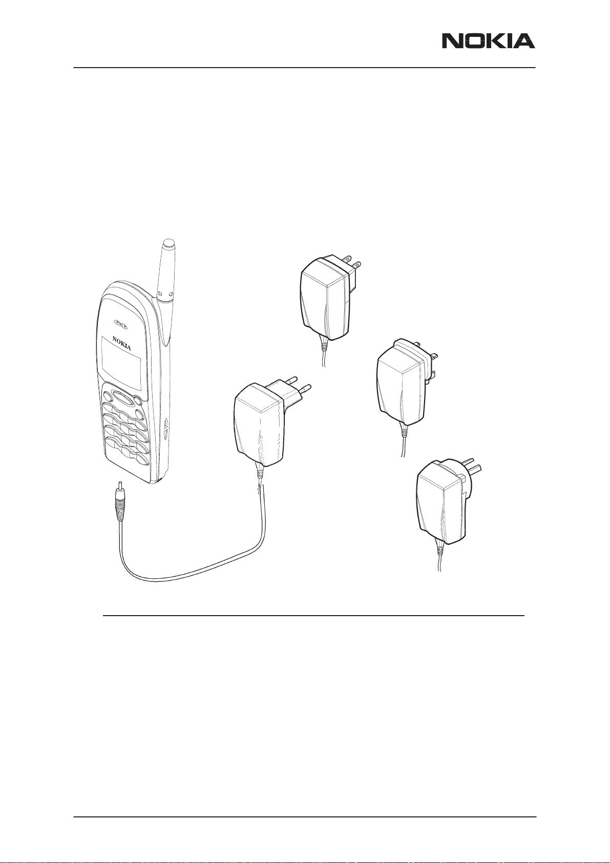
Product Selection
Handportable
THF–13 is a small and light handportable phone working in the NMT450
network. The product is based on the DCT3 mechanics (batteries) and
user interface (UI), The electronics and features are modified for
NMT450 DOC 3 specification
1.
PAMS Technical Documentation
ACP–8U
4.
ACP–8X
ACP–8E
5.
2.
ACP–8A
3.
6.
Item Name: Type code: Material code:
1. Transceiver (See variant Appendices)
2. Standard battery (NiMH 900 mAh) BMS–2 0671323
3. Performance Travel Charger
4. Performance Travel Charger US plug 90-264 Vac ACP-8U 0675196
5. Performance Travel Charger
6. Performance Travel Charger Australia plug 90-264 Vac ACP-8A 0675214
Page 4
Nokia Mobile Phones Ltd.
Euro plug 90-264 Vac ACP-8E 0675195
UK plug 90-264 Vac ACP-8X 0675197
Issue 1 08/99
Page 5
PAMS Technical Documentation
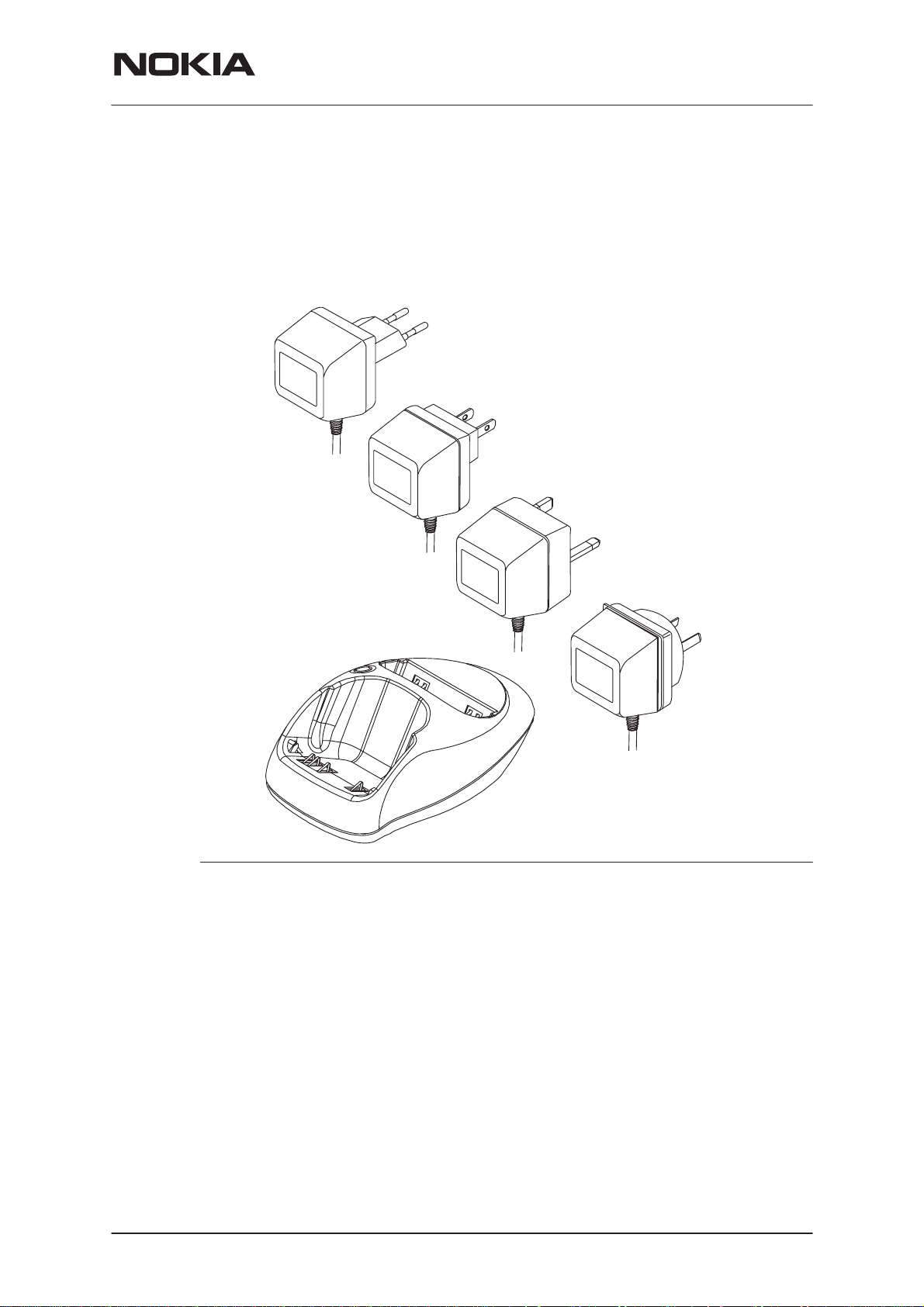
Desktop Option
The desktop option allows the user to charge the handportable and spare
battery from mains. With this option the user can also discharge the spare
battery. The desktop option contains the following products:
2.
THF-13
General Information
3.
4.
1.
5.
1. Desktop stand DCH–9 0700049
2. AC Travel Charger
3. AC Travel Charger (US plug) 108–132 Vac ACP–7U 0675143
AC Travel Charger (US plug) 207–253 Vac ACP–7P 0675147
AC Travel Charger (US plug) 198–242 Vac ACP–7C 0675158
4. AC Travel Charger
AC Travel Charger (UK plug) 180–220 Vac ACP–7H 0675146
5. AC Travel Charger (Australia) 216–264 Vac ACP–7A 0675148
(Euro plug) 207–253 Vac ACP–7E 0675144
(UK plug) 207–253 Vac ACP–7X 0675145
Issue 1 08/99
Nokia Mobile Phones Ltd.
Page 5
Page 6
THF-13
General Information
Basic Car Kit (CARK–64) Option
PAMS Technical Documentation
1.
4.
3.
2.
Item Name: Type code: Material code:
1. Transceiver (See variant Appendices)
2. Mobile Holder MBC–1 0700060
3. Cigarette Lighter Charger LCH–9 0657120
4. Swivel Mount HHS–9 0620037
Page 6
Nokia Mobile Phones Ltd.
Issue 1 08/99
Page 7

THF-13
PAMS Technical Documentation
General Information
Advanced Hands Free Car Installation (CARK–91) Option
7.
8.
3.
2.
6.
1.
5.
4.
Item/name: Type code: Material code:
1. Transceiver (See variant Appendices)
2. Mobile Holder MCC–1 0620043
3. Hands Free Unit HFU–2 0694049
4. Hands Free Microphone HFM–8 0690016
5. Hands Free Speaker HFS–12 0692008
6. Power Cable PCH–4J 0730055
7. Swivel Mount HHS–9 0620037
8. Mounting Plate MKU–1 0620036
Issue 1 08/99
Nokia Mobile Phones Ltd.
Page 7
Page 8

THF-13
General Information
Module and Product Lists
PAMS Technical Documentation
Name of module Type des. Material
code
Transceiver THF–13 0503089 Handportable phone
User interface module NU1 0201258
System/RF module NH2 0201468
Assembly parts MTHF12 0262060 Basic
Antenna AHN–4 0660185
Battery pack BMS–2 0670203 Battery pack, 900 mAh; NiMH
Battery pack BMS–2S 0670225 Standard battery pack, 900 mAh; NiMH
Battery pack BMS–2V 0670204 V ibra battery pack, 900 mAh; NiMH
Battery pack BLS–4 0670207 Extended battery pack, 1600 mAh; Li–ion
Battery pack BLS–2H 0670235 Slim battery pack, 900 mAh; Li–ion
Fast charger ACP–9E 0675149 DIN
Fast charger ACP–9X 0675150 UK
Slow charger ACP–7E 0675144 DIN
Slow charger ACP–7X 0675145 UK
Desk Stand DCH–9 0700049
Headset HDC–9 0694053
Inductive loopset LPS–1 0630146
Data cable DKT–5 0730164 for Smart Modular Technologies PCMCIA
Basic Car Mount MBC–1 0700060
Swivel mount HHS–9 0620037
Cig.lighter cable LCH–9 0675120
Advanced car holder MCC–1 0629943
Advanced HF unit HFU–2 0694049
Power cable PCH–4J 0730055
Mounting plate MKU–1 0620036
Swivel mount HHS–9 0620037
HF Microphone HFM–8 0690016
HF speaker HSS–12 0692008
Handset HSU–1 0640047
Booster adapter BSA–2 0770166
Notes
Page 8
Nokia Mobile Phones Ltd.
Issue 1 08/99
Page 9

PAMS Technical Documentation
Technical Specifications
General Specifications of Transceiver THF–13
Parameter Notes
Cellular system NMT450
TX frequency band 453.000–457.475MHz
RX frequency band 463.000–467.475MHz
Duplex spacing 10 MHz
Number of RF channels 180
Channel spacing 25 kHz
Maximum output power 1.5W
THF-13
General Information
Method of frequency sythesis Dual direct PLL
Power Supply Voltage 3.2... 5.3 V
Technological improvements in the THF-13 are the nominal battery voltage which is 3.6 V and operating voltage on logic chips , 2.8 V. The
ROMless CPU necessitates the use of an external program memory
(flash).
The transceiver consist of four modules: UIF module, rf/system module,
battery pack and mechanics.
The user interface has fully graphical LCD–display and keybord with side
volume keys.
Table 1. Mechanical Characteristics
Unit Dimensions
(mm) (W x H x
D)
Transceiver with standard
battery pack BMS–2
Transceiver with Antenna 48 x 174/297 x
Battery pack 900 mAh
BLS–2
Battery pack 1500 mAh
BLS–4
48 x 136 x 32 137 Dimensions without antenna
32
depth 28
depth 35
Weight
(g)
Vol-
ume
(cm3)
Notes
Height dimension antenna in
and rectractable
Modes of Operation
Standby, listening and conversation
Issue 1 08/99
Nokia Mobile Phones Ltd.
Page 9
Page 10

THF-13
General Information
PAMS Technical Documentation
Maximum ratings
Parameter Rating
Battery voltage, idle mode 3.2 ... 5.3 V (5.0V in call mode with charger)
Charger input voltage –5.0 ... 16V
Operating temperature range –25C to +55C
Storage temperature range –40C to +85 C
DC Characteristics
Line Symbol Minimum Typical /
Nominal
Supply battery voltage 3.3 3.6 5.3 V
Battery cut off voltage (HW) 2.7 2.8 2.9 V (3.3V min SW
Regulated logic supply voltage (VL) 2.7 2.8 2.85 V
Regulated logic supply current 0 40 mA
Regulated audio supply voltage (VA) 2.7 2.8 2.85 V
Regulated audio supply current 0 100 mA
Regulated RX supply voltage (VRX) 2.7 2.8 2.85 V
Regulated RX supply current 0.05 50 mA
Regulated TX supply voltage (VTX) 2.7 2.8 2.85 V
Regulated TX supply current 0.02 60 mA
Current consumption standby mode mA
Current consumption sleep mode mA
Current consumption conv. low power mA
Current consumption conv. high power mA
Maximum Unit / Notes
cutoff)
AC Characteristics
General RF specifications:
Parameter Rating
TX frequency band 453.000–457.475MHz
RX frequency band 463.000–467.475MHz
Duplex spacing 10 MHz
Number of RF channels 180
Channel spacing 25 kHz
Signalling 1200 Baud FFSK
Page 10
Nokia Mobile Phones Ltd.
Issue 1 08/99
Page 11

PAMS Technical Documentation
ratio
Transmitter branch specifications:
Parameter Rating
Frequency band 453.000–457.475MHz
Output RF power 0.15 or 0.75 W
THF-13
General Information
Spurious signals (TX ON)
Spurious signals (STANDBY)
Modulation method FM
Deviation 4.7 kHz max
Deviation with supervisory signal 5.0 kHz max
FFSK deviation 1200 Hz (”1”)
1800 Hz (”0”)
Harmonic distortion < 5 %
Audio Frequency responce 300–500 Hz
500–2000 Hz
2–3 KHz
pre–emphasis
Adjacent Channel Power < –70 dBc
Audio Intermodulation products < –20 dB
Residual Modulation linear
psophometric
< 0.25 uW, f = 100kHz – 1GHz
< 1 uW, f = 1GHz – 4GHz
< 2 nW, f = 100kHz – 1GHz
< 20 nW, f = 1GHz – 4GHz
2800 Hz dev. +/– 400 Hz
4200 Hz dev. +/– 600 Hz
+1–3 dB
+/– 1 dB
+1–3 dB
6 dB/Oct
< –20 dB (peak)
< –40 dB (rms)
Audio Muting > 40 dB
Compander SW enabled compression
dynamic range
Output RF power 0.75 W
Number of power levels 3
Frequency error +/– 2.5 kHz
2:1
3 – –50 dB +/– 1 dB
Receiver branch specifications:
Parameter Rating
Frequency band 463.000–467.475MHz
Sensitivity –113 dBm (20 dB SINAD psoph. )
Adjacent Channel Selectivity > 67 dB
Spurious Responce Rejection > 67 dB
Intermodulate Rejection > 67 dB
Blocking > 87 dB
Issue 1 08/99
Nokia Mobile Phones Ltd.
Page 11
Page 12

THF-13
ratio
General Information
PAMS Technical Documentation
RatingParameter
Spurious signals (TX OFF)
Audio Intermodulation Products < –20 dB ( refer to 1600 Hz)
AM suppression > 30 dB
Hum and Noise linear
phopsometric
Audio Frequency responce 300–500 Hz
500–2000 Hz
2–3 KHz
de–emphasis
Harmonic distortion <5 %
Audio Muting > 50 dB
Expander SW enabled compression
dynamic range
RSSI dynamic range 60 dB
< 2 nW, f = 100kHz – 1GHz
< 20 nW, f = 1GHz – 4GHz
< –20 dB (peak to peak)
< –40 dB (rms)
+1–3 dB
+/– 1 dB
+1–3 dB
6 dB/Oct
1:2
3 – –50 dB +/– 1 dB
TX synthesizer specifications:
Parameter Rating
Transmitted frequency difference from BS in
conversation mode
Frequency range 453.000–457.475MHz
Output level 4 +/– 2 dB (BST off) , 8 +/–2 dB (BST on)
Phase Noise < –1 18 dBc/Hz (@25KHz)
Settling Time CHN–>CHN+? < 35 ms
+/– 2.5 k Hz
RX synthesizer specifications:
Parameter Rating
Frequency Tolerance at Startup +/– 2.5 ppm
Frequency range 418.000–422.475MHz
Output level 1 +/– 3 dB
Phase Noise < –1 18 dBc/Hz (@25KHz)
Settling Time CHN–>CHN+? < 25 ms
Page 12
Nokia Mobile Phones Ltd.
Issue 1 08/99
Page 13

PAMS Technical Documentation
External Connections
THF-13
General Information
Battery connectors
RF connector
System connector Charging connector
mic
Issue 1 08/99
Nokia Mobile Phones Ltd.
Page 13
Page 14

THF-13
General Information
System connector
Contact 1
PAMS Technical Documentation
Rubber boot
Microphone
Solderable element,
2 pcs
DC–jack
Contact 2
Microphone port
Contacts
3...8
Contact 9
Cable/Cradle connector
guiding/fixing hole, 3 pcs
The bottom connector (pins listed in the table below) includes the following parts:
– DC connector for external plug–in charger and a desktop charger
– System connector for accessories and intelligent battery packs
– Internal microphone with spring contacts
Contact Line Symbol Function
1 VIN Charger input voltage
DC–jack
side contact
(DC–plug ring)
DC–jack
center pin
DC–jack
side contact
(DC–plug jacket)
2 CHRG_CTRL Charger control output (from phone)
L_GND Charger ground
VIN Charger input voltage
CHRG_CTRL Charger control output (from phone)
Microphone
acoustic ports
3 XMIC Accessory microphone signal input (to phone)
4 SGND Accessory signal ground
5 XEAR Accessory earphone signal output (from phone)
6 MBUS MBUS, bidirectional serial data i/o
Page 14
Nokia Mobile Phones Ltd.
Acoustic signal (to phone)
Issue 1 08/99
Page 15

PAMS Technical Documentation
C
FunctionLine SymbolContact
7 FBUS_RX FBUS, unidirectional serial data input (to phone)
8 FBUS_TX FBUS, unidirectional serial data output (from phone)
9 L_GND Charger ground
General Information
The electrical specifications below list the bottom connector signals and
levels in the baseband. The system connector is used to connect the
transceiver to accessories. The System connector pins can also be used
to connect intelligent battery packs to the transceiver. The table gives the
idle voltage produced by the acceptable chargers at the DC connector input. The absolute maximum input voltage is 30 V due to the transient
suppressor that is protecting the charger input.
Table 2. Signals of the bottom connector
THF-13
Pin Name Min Typ Max Unit Notes
1,3 VIN
2 L_GND 0 0 V Supply ground
4,5 CHRG_
TRL
6 MICP N/A see section Internal microphone
7 MICN N/A see section Internal microphone
8 XMIC
7.25
3.25
320
7.1
3.25
720
0 0.5 V Charger control PWM low
2.0 2.85 V Charger control PWM high
1 99 % PWM duty cycle
2.0 2.2 kΩ Input AC impedance
7.6
3.6
370
8.4
3.6
800
32 Hz PWM frequency for a fast charger
7.95
16.9
3.95
420
9.3
3.95
850
V
V
V
mA
V
V
mA
Unloaded ACP–7 Charger (5kohms
load)
Peak output voltage (5kohms load)
Loaded output voltage (10ohms load)
Supply current
Unloaded ACP–9 Charger
Loaded output voltage (10ohms load)
Supply current
1 Vpp Maximum signal level
1.47 1.55 V Mute (output DC level)
2.5 2.85 V Unmute (output DC level)
100 600 µA Bias current
58 490 mV Maximum signal level
9 SGND
Issue 1 08/99
47 Ω Output AC impedance (ref. GND)
10 µF Series output capacitance
380 Ω Resistance to phone ground
Nokia Mobile Phones Ltd.
Page 15
Page 16

THF-13
Baud rate 9600 Bit/s
2.0
logic high
2.85
2.0
logic high
2.85
General Information
PAMS Technical Documentation
Table 2. Signals of the bottom connector (continued)
NotesUnitMaxTypMinNamePin
10 XEAR
16 300 Ω Load AC impedance to SGND (Head-
4.7 10 kΩ Load AC impedance to SGND (Acces-
16 1500 Ω Load DC resistance to SGND (Head-
11 MBUS 0 logic low
2.0 logic high 2.85
12 FBUS_RX
/
BOOST0
0
47 Ω Output AC impedance (ref. GND)
10 µF Series output capacitance
1.0 Vpp Maximum output level (no load)
22 626 mV Output signal level
10 kΩ Load DC resistance to SGND (Acces-
2.8 V DC voltage (47k pull–up to VBB)
logic low
set)
sory)
sory)
set)
0.8 V Serial bidirectional control bus.
Phone has a 4k7 pullup resistor
0.8
V Fbus receive. Serial Data
Baud rate 9.6k–230.4kBit/s
Phone has a 100k pulldown resistor
RF booster control line
13 FBUS_TX
/
BOOST1
14 GND 0 0.3 V Supply ground
0
logic low
0.5
V Fbus transmit. Serial Data
Baud rate 9.6k–230.4kBit/s
Phone has a 100k pullup resistor
RF booster control line
An external headset device is connected to the system connector XMIC,
SGND and XEAR lines, from which the signals are routed to the MASI
ASIC microphone inputs and external earphone outputs.
For protection against ESD spikes at the system connector, the data
transmission lines (MBUS, RX and TX) are equipped with an ESD protection circuit.
Page 16
Nokia Mobile Phones Ltd.
Issue 1 08/99
Page 17

PAMS Technical Documentation
General Information
Battery connector
The electrical specifications for the battery connector is shown in the next
table.
Table 3. Battery Connector Electrical Specifications
Pin Name Min Typ Max Unit Notes
1 BVOLT 3.2 3.6 4.5 V Battery voltage
5.3 Maximum voltage in idle state with charger
2 BSI
3 BTEMP
0 2.85 V Battery size indication
Phone has 47kohm pull up resistor.
2.2 18 kohm Battery indication resistor (Ni battery)
20 22 24 kohm Battery indication resistor (service battery)
27 51 kohm Battery indication resistor (4.1V Lithium
battery)
68 91 kohm Battery indication resistor (4.2V Lithium bat-
tery)
0 1.4 V Battery temperature indication
Phone has a 100k (+–5%) pullup resistor,
Battery package has a NTC pulldown resis-
tor:
47k+–5%@+25C , B=4050+–3%
THF-13
2.1
5 10
1.9
90 100
0 1 kohm Local mode initialization (in production)
20 22 25 kHz PWM control to VIBRA BATTERY
4 BGND 0 0 V Battery ground
3
20
2.85
200
V
ms
V
ms
Phone power up by battery (input)
Power up pulse width
Battery power up by phone (output)
Power up pulse width
Issue 1 08/99
Nokia Mobile Phones Ltd.
Page 17
Page 18

THF-13
General Information
Functional Description
Circuit Description
The transceiver electronics consist of a UI module PCB and a RF/system
PCB. The UI module is connected to the system module with a connector. The System and rf submodules are interconnected with PCB wiring.
The unit can be connected to accessories with a bottom system connector, which includes charging and accessory control.
The RF block is designed for a hand portable phone operating in NMT450
systems. The purpose of the RF module is to receive and demodulate
radio frequency signal from a base station and to transmit a modulated
RF signal to a base station.
PAMS Technical Documentation
Block Diagram
The THF–13 consist of 2 pcbs, NH1 and NU1. The NH1 consist of 2 submodules, BASEBAND and RF. The BASEBAND consist of 3 functional
blocks: PWRU, CTRLU and AUDIO and RF consist of 3 ones: RX, SYNT,
TX. NU1 is the User Interface module (UIF–module).
PWRU
CTRLU
BASEBAND–submodule
AUDIO
RX
SYNT
TX
RF–submodule
ANT
DUP
Page 18
UIF–module
LCDLCD
LCD Driver
THF–13 Block Diagram
Nokia Mobile Phones Ltd.
BUZZER
MIC,EAR
Issue 1 08/99
Page 19

PAMS Technical Documentation
Interconnection Diagram
THF-13
General Information
Keypad Display
10 9
User Interface
Module
NU1
4
Battery
System/RF
Module
NH1
622 3+3
Mic
Connector
RF
Charger
2
Earpiece
Antenna
1
System
Connector
Issue 1 08/99
Nokia Mobile Phones Ltd.
Page 19
Page 20

THF-13
General Information
Power Distribution Diagram
PAMS Technical Documentation
VCS
VBAT
PWRU
VRX
VTX
VL
VA
CTRLU
RECEIVER
AUDIO
TRANSMITTERSYNTHESIZER
LCD Driver
UIF–module
LCDLCD
Page 20
Nokia Mobile Phones Ltd.
Issue 1 08/99
 Loading...