

Page 1

PAMS Technical Documentation
THF-12 Series Transceivers
Chapter 2
System Module NH1
Issue 3 02/2000 Nokia Mobile Phones Ltd.
Page 2
THF-12
System Module NH1
PAMS Technical Documentation
AMENDMENT RECORD SHEET
Amendment
Number
Date Inserted By Comments
02/99 OJuntune Original
Issue2 05/99 OJuntune P.8, 11, 12, 25, 26, 44, 45, 47, 52, 53
57 values amended or updated
NH1 v. 4.11 added
A3 schematics updated
Table of contents updated
Amendment record sheet updated
Issue3 02/2000 OJuntune NH1 v. 4.14 added p.83–94
Table of contents p.5 updated
Amendment record sheet updated
Page 2
Nokia Mobile Phones Ltd.
Issue 3 02/2000
Page 3

PAMS Technical Documentation
CONTENTS
Transceiver THF–12 System Module NH1 2 – 7. . . . . . . . . . . . . . . . . .
Introduction 2 – 7. . . . . . . . . . . . . . . . . . . . . . . . . . . . . . . . . . . . . . . . . .
System Module 2 – 7. . . . . . . . . . . . . . . . . . . . . . . . . . . . . . . . . . . .
Baseband Sub-module 2 – 8. . . . . . . . . . . . . . . . . . . . . . . . . . . . . . . . . .
Technical summary 2 – 10. . . . . . . . . . . . . . . . . . . . . . . . . . . . . . . . . . .
Modes of Operation 2 – 10. . . . . . . . . . . . . . . . . . . . . . . . . . . . . . . . . . .
Technical Specifications 2 – 11. . . . . . . . . . . . . . . . . . . . . . . . . . . . .
Maximum Ratings 2 – 11. . . . . . . . . . . . . . . . . . . . . . . . . . . . . . . .
DC Characteristics 2 – 11. . . . . . . . . . . . . . . . . . . . . . . . . . . . . . .
Battery connector 2 – 11. . . . . . . . . . . . . . . . . . . . . . . . . . . . . . . . . .
UIF–connector 2 – 12. . . . . . . . . . . . . . . . . . . . . . . . . . . . . . . . . . . . .
CTRLU Circuit 2 – 13. . . . . . . . . . . . . . . . . . . . . . . . . . . . . . . . . . . . .
Block Description 2 – 13. . . . . . . . . . . . . . . . . . . . . . . . . . . . . . . . . .
CTRLU – CONNECTORU 2 – 13. . . . . . . . . . . . . . . . . . . . . . . .
CTRLU – PWRU 2 – 13. . . . . . . . . . . . . . . . . . . . . . . . . . . . . . . . .
CTRLU – AUDIO 2 – 14. . . . . . . . . . . . . . . . . . . . . . . . . . . . . . . .
CTRLU – UIF 2 – 14. . . . . . . . . . . . . . . . . . . . . . . . . . . . . . . . . . .
CTRLU – RX 2 – 14. . . . . . . . . . . . . . . . . . . . . . . . . . . . . . . . . . . .
CTRLU – SYNT 2 – 14. . . . . . . . . . . . . . . . . . . . . . . . . . . . . . . . .
CTRLU – TX 2 – 15. . . . . . . . . . . . . . . . . . . . . . . . . . . . . . . . . . . .
Main Components 2 – 15. . . . . . . . . . . . . . . . . . . . . . . . . . . . . . .
Controller Ports 2 – 15. . . . . . . . . . . . . . . . . . . . . . . . . . . . . . . . . .
PWRU 2 – 19. . . . . . . . . . . . . . . . . . . . . . . . . . . . . . . . . . . . . . . . . . . .
Power Distribution 2 – 19. . . . . . . . . . . . . . . . . . . . . . . . . . . . . . .
Battery charging 2 – 19. . . . . . . . . . . . . . . . . . . . . . . . . . . . . . . . .
Startup charging 2 – 20. . . . . . . . . . . . . . . . . . . . . . . . . . . . . . . . .
Battery overvoltage protection 2 – 21. . . . . . . . . . . . . . . . . . . . .
Battery removal during charging 2 – 22. . . . . . . . . . . . . . . . . . .
Different PWM frequencies ( 1Hz and 32 Hz) 2 – 22. . . . . . . .
Supply voltage regulators and controlling 2 – 24. . . . . . . . . . .
Operation modes 2 – 28. . . . . . . . . . . . . . . . . . . . . . . . . . . . . . . .
Power–Off Mode 2 – 28. . . . . . . . . . . . . . . . . . . . . . . . . . . . . . . . .
Entering Power–Off Mode 2 – 28. . . . . . . . . . . . . . . . . . . . . . . . .
Charging in Power–Off 2 – 29. . . . . . . . . . . . . . . . . . . . . . . . . . .
Reset Mode 2 – 29. . . . . . . . . . . . . . . . . . . . . . . . . . . . . . . . . . . . .
Power–On Mode 2 – 30. . . . . . . . . . . . . . . . . . . . . . . . . . . . . . . . .
AUDIO BLOCK 2 – 31. . . . . . . . . . . . . . . . . . . . . . . . . . . . . . . . . . . . . . .
Main features 2 – 31. . . . . . . . . . . . . . . . . . . . . . . . . . . . . . . . . . .
FFSK modem features 2 – 31. . . . . . . . . . . . . . . . . . . . . . . . . . .
Audio features 2 – 31. . . . . . . . . . . . . . . . . . . . . . . . . . . . . . . . . . .
Other features 2 – 31. . . . . . . . . . . . . . . . . . . . . . . . . . . . . . . . . . .
THF-12
System Module NH1
Page No
Issue 3 02/2000
Nokia Mobile Phones Ltd.
Page 3
Page 4

THF-12
System Module NH1
Receive (RX) Audio Signal Path 2 – 35. . . . . . . . . . . . . . . . . . . . . . . .
Receiving Data Path 2 – 35. . . . . . . . . . . . . . . . . . . . . . . . . . . . .
Receiving Audio Path 2 – 35. . . . . . . . . . . . . . . . . . . . . . . . . . . .
RX Trimmer 2 – 36. . . . . . . . . . . . . . . . . . . . . . . . . . . . . . . . . . . . .
Mux and de–emphasis 2 – 36. . . . . . . . . . . . . . . . . . . . . . . . . . .
Expander 2 – 36. . . . . . . . . . . . . . . . . . . . . . . . . . . . . . . . . . . . . . .
RX filter 2 – 36. . . . . . . . . . . . . . . . . . . . . . . . . . . . . . . . . . . . . . . .
De–scrambler 2 – 36. . . . . . . . . . . . . . . . . . . . . . . . . . . . . . . . . . .
RX automatic gain control 2 – 36. . . . . . . . . . . . . . . . . . . . . . . . .
Ear sensitive filter 2 – 37. . . . . . . . . . . . . . . . . . . . . . . . . . . . . . . .
Volume control 2 – 37. . . . . . . . . . . . . . . . . . . . . . . . . . . . . . . . . .
Earphone and accessory buffers 2 – 37. . . . . . . . . . . . . . . . . . .
Transmitting paths 2 – 37. . . . . . . . . . . . . . . . . . . . . . . . . . . . . . .
Transmitting data path 2 – 37. . . . . . . . . . . . . . . . . . . . . . . . . . . .
Transmitting audio path 2 – 37. . . . . . . . . . . . . . . . . . . . . . . . . . .
Mic amplifier and mux 2 – 38. . . . . . . . . . . . . . . . . . . . . . . . . . . .
Mic trimmer and bandpass filter 2 – 38. . . . . . . . . . . . . . . . . . . .
Scrambler 2 – 38. . . . . . . . . . . . . . . . . . . . . . . . . . . . . . . . . . . . . .
Compressor 2 – 38. . . . . . . . . . . . . . . . . . . . . . . . . . . . . . . . . . . . .
Pre–emphasis 2 – 38. . . . . . . . . . . . . . . . . . . . . . . . . . . . . . . . . . .
Automatic Gain Control 2 – 39. . . . . . . . . . . . . . . . . . . . . . . . . . .
Tx hard limiter 2 – 39. . . . . . . . . . . . . . . . . . . . . . . . . . . . . . . . . . .
Tx lowpass filter 2 – 39. . . . . . . . . . . . . . . . . . . . . . . . . . . . . . . . .
Tx audio level control 2 – 39. . . . . . . . . . . . . . . . . . . . . . . . . . . . .
Tx trimmer 2 – 39. . . . . . . . . . . . . . . . . . . . . . . . . . . . . . . . . . . . . .
Summing unit and trimmer 2 – 39. . . . . . . . . . . . . . . . . . . . . . . .
FII path 2 – 39. . . . . . . . . . . . . . . . . . . . . . . . . . . . . . . . . . . . . . . . . . .
Fii filtering and gain control 2 – 39. . . . . . . . . . . . . . . . . . . . . . . .
Hands free system 2 – 39. . . . . . . . . . . . . . . . . . . . . . . . . . . . . . . . .
Hands free controller 2 – 40. . . . . . . . . . . . . . . . . . . . . . . . . . . . .
Hands free attenuators 2 – 40. . . . . . . . . . . . . . . . . . . . . . . . . . .
Buzzer driver 2 – 40. . . . . . . . . . . . . . . . . . . . . . . . . . . . . . . . . . . . . .
Clock divider 2 – 40. . . . . . . . . . . . . . . . . . . . . . . . . . . . . . . . . . . . . .
Call continue sensor 2 – 41. . . . . . . . . . . . . . . . . . . . . . . . . . . . . . . .
FM radio 2 – 41. . . . . . . . . . . . . . . . . . . . . . . . . . . . . . . . . . . . . . . . . .
RF Module 2 – 42. . . . . . . . . . . . . . . . . . . . . . . . . . . . . . . . . . . . . . . . . .
Introduction 2 – 42. . . . . . . . . . . . . . . . . . . . . . . . . . . . . . . . . . . . . . .
Technical Specifications 2 – 44. . . . . . . . . . . . . . . . . . . . . . . . . . . . .
Maximum ratings 2 – 44. . . . . . . . . . . . . . . . . . . . . . . . . . . . . . . .
RX 2 – 44. . . . . . . . . . . . . . . . . . . . . . . . . . . . . . . . . . . . . . . . . . . . .
SYNT 2 – 44. . . . . . . . . . . . . . . . . . . . . . . . . . . . . . . . . . . . . . . . . .
TX 2 – 44. . . . . . . . . . . . . . . . . . . . . . . . . . . . . . . . . . . . . . . . . . . . .
Current Consumption 2 – 45. . . . . . . . . . . . . . . . . . . . . . . . . . . . . . .
Connections 2 – 47. . . . . . . . . . . . . . . . . . . . . . . . . . . . . . . . . . . . . . . . .
Connections to Baseband sub–module 2 – 47. . . . . . . . . . . . . . . .
Antenna 2 – 50. . . . . . . . . . . . . . . . . . . . . . . . . . . . . . . . . . . . . . . . . .
PAMS Technical Documentation
Page 4
Nokia Mobile Phones Ltd.
Issue 3 02/2000
Page 5

PAMS Technical Documentation
Receiver 2 – 50. . . . . . . . . . . . . . . . . . . . . . . . . . . . . . . . . . . . . . . . . .
RX Synthesizer 2 – 50. . . . . . . . . . . . . . . . . . . . . . . . . . . . . . . . . . . .
RX loop filter 2 – 51. . . . . . . . . . . . . . . . . . . . . . . . . . . . . . . . . . . .
TX Synthesizer 2 – 51. . . . . . . . . . . . . . . . . . . . . . . . . . . . . . . . . . . . . . .
TX Loop Filter 2 – 52. . . . . . . . . . . . . . . . . . . . . . . . . . . . . . . . . . .
Transmitter 2 – 52. . . . . . . . . . . . . . . . . . . . . . . . . . . . . . . . . . . . . . . .
RF Characteristics 2 – 52. . . . . . . . . . . . . . . . . . . . . . . . . . . . . . . . . . . .
Ambient temperature 2 – 52. . . . . . . . . . . . . . . . . . . . . . . . . . . . . . .
Duplexer 2 – 52. . . . . . . . . . . . . . . . . . . . . . . . . . . . . . . . . . . . . . . . . .
RX submodule 2 – 53. . . . . . . . . . . . . . . . . . . . . . . . . . . . . . . . . . . . .
Preamplifier 2 – 54. . . . . . . . . . . . . . . . . . . . . . . . . . . . . . . . . . . . .
RX–filter 2 – 54. . . . . . . . . . . . . . . . . . . . . . . . . . . . . . . . . . . . . . . .
1st mixer 2 – 54. . . . . . . . . . . . . . . . . . . . . . . . . . . . . . . . . . . . . . .
1st IF–filter 2 – 55. . . . . . . . . . . . . . . . . . . . . . . . . . . . . . . . . . . . . .
IF–amplifier 2 – 55. . . . . . . . . . . . . . . . . . . . . . . . . . . . . . . . . . . . .
2nd IF–filter 2 – 56. . . . . . . . . . . . . . . . . . . . . . . . . . . . . . . . . . . . .
IF–circuit 2 – 56. . . . . . . . . . . . . . . . . . . . . . . . . . . . . . . . . . . . . . .
TX submodule 2 – 57. . . . . . . . . . . . . . . . . . . . . . . . . . . . . . . . . . . . .
Power amplifier 2 – 57. . . . . . . . . . . . . . . . . . . . . . . . . . . . . . . . . .
Power control 2 – 58. . . . . . . . . . . . . . . . . . . . . . . . . . . . . . . . . . .
Coupler lines 2 – 58. . . . . . . . . . . . . . . . . . . . . . . . . . . . . . . . . . . .
Synthesizer submodule 2 – 58. . . . . . . . . . . . . . . . . . . . . . . . . . . . .
PLL 2 – 58. . . . . . . . . . . . . . . . . . . . . . . . . . . . . . . . . . . . . . . . . . . .
RX VCO 2 – 59. . . . . . . . . . . . . . . . . . . . . . . . . . . . . . . . . . . . . . . .
TX VCO 2 – 59. . . . . . . . . . . . . . . . . . . . . . . . . . . . . . . . . . . . . . . .
Isolation amplifier (TX buffer) 2 – 60. . . . . . . . . . . . . . . . . . . . . .
VCTCXO 2 – 60. . . . . . . . . . . . . . . . . . . . . . . . . . . . . . . . . . . . . . .
THF-12
System Module NH1
Parts list of NH1 Basic (EDMS Issue 4.5) Code: 0201267 2 – 72. . . .
Parts list of NH1 Basic (EDMS Issue 4.11) Code: 0201267 2 – 61. . .
Parts list of NH1 Basic (EDMS Issue 4.14) Code: 0201267 2 – 83. . .
Schematic Diagrams
Block Diagram of System/RF Blocks (Version 12 Edit 164)
for layout version 12 and 15 3A–2. . . . . . . . . . . . . . . . . . . . . . . . . . . . .
Circuit Diagram of Connectors (Version 12 Edit 244)
for layout version 12 3A–3. . . . . . . . . . . . . . . . . . . . . . . . . . . . . . . . . . . .
Circuit Diagram of CTRLU Block (Version 12 Edit 235 )
for layout version 12 3A–4. . . . . . . . . . . . . . . . . . . . . . . . . . . . . . . . . . .
Circuit Diagram of PWRU (Version 13 Edit 216 )
for layout version 12 3A–5. . . . . . . . . . . . . . . . . . . . . . . . . . . . . . . . . . . .
Circuit Diagram of Audio (Version 12 Edit 315)
for layout version 12 3A–6. . . . . . . . . . . . . . . . . . . . . . . . . . . . . . . . . . . . .
Page No
Issue 3 02/2000
Nokia Mobile Phones Ltd.
Page 5
Page 6

THF-12
System Module NH1
Circuit Diagram of Receiver (Version 07 Edit 171)
for layout version 12 3A–7. . . . . . . . . . . . . . . . . . . . . . . . . . . . . . . . . . . . .
Circuit Diagram of Synthesiser Block (Version 07 Edit 90)
for layout version 12 3A–8. . . . . . . . . . . . . . . . . . . . . . . . . . . . . . . . . . . . .
Circuit Diagram of Transmitter (Version 07 Edit 171)
for layout version 12 3A–9. . . . . . . . . . . . . . . . . . . . . . . . . . . . . . . . . . . . .
Layout Diagram of NH1 (Version 12) 3A–10. . . . . . . . . . . . . . . . . . . . . .
Circuit Diagram of Connectors (Version 15 Edit 245)
for layout version 15 3A–11. . . . . . . . . . . . . . . . . . . . . . . . . . . . . . . . . . . . .
Circuit Diagram of Audio (Version 15 Edit 317)
for layout version 15 3A–12. . . . . . . . . . . . . . . . . . . . . . . . . . . . . . . . . . . .
Circuit Diagram of PWRU (Version 15 Edit 220 )
for layout version 15 3A–13. . . . . . . . . . . . . . . . . . . . . . . . . . . . . . . . . . . . .
Circuit Diagram of CTRLU Block (Version 15 Edit 236 )
for layout version 15 3A–14. . . . . . . . . . . . . . . . . . . . . . . . . . . . . . . . . . . .
PAMS Technical Documentation
Circuit Diagram of Receiver (Version 15 Edit 172)
for layout version 15 3A–15. . . . . . . . . . . . . . . . . . . . . . . . . . . . . . . . . . . . .
Circuit Diagram of Synthesiser Block (Version 15 Edit 96)
for layout version 15 3A–16. . . . . . . . . . . . . . . . . . . . . . . . . . . . . . . . . . . . .
Circuit Diagram of Transmitter (Version 15 Edit 175)
for layout version 15 3A–17. . . . . . . . . . . . . . . . . . . . . . . . . . . . . . . . . . . . .
Layout Diagram of NH1 (Version 15) 3A–18. . . . . . . . . . . . . . . . . . . . . .
Page 6
Nokia Mobile Phones Ltd.
Issue 3 02/2000
Page 7
PAMS Technical Documentation
System Module NH1
Transceiver THF–12 System Module NH1
Introduction
This document specifices the System module NH1 of the THF–12
NMT–450 cellular phone.
The NH1 System Module comprises the baseband and the RF functions
of the phone.
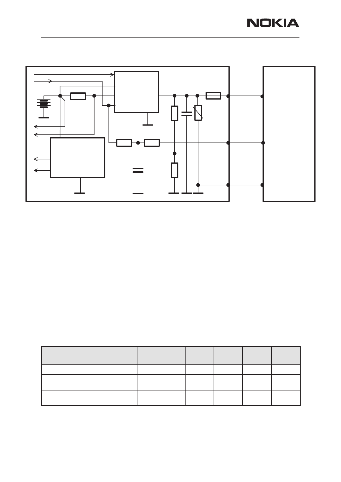
System Module
Name of submodule Notes
THF-12
CTRLU
CONNU
PWRU
AUDIO
RX
TX
SYNT
Control Unit for the phone
Connector Unit
Power supply
Audio
Receiver
Transmitter
Synthesizer
These blocks are only functional blocks and therefore have no type nor
material codes.
Issue 3 02/2000
Nokia Mobile Phones Ltd.
Page 7
Page 8

THF-12
System Module NH1
Baseband Sub-module
The Baseband submodule controls the internal operation of the phone. It
controls the user interface, i.e. LCD driver, keyboard and audio interface
functions. The module performs all signalling towards the system and car-
ries out audio–frequency signal processing. In addition, it controls the op-
eration of the transceiver and stores tuning data for the phone.
The baseband architecture is basically similar to the previous generation.
However, the system specified logical voltage level used is 2.82V and
new features include a improved charging circuit CHAPS, a new power
supply circuit PSA and signalling ASIC MASI.
The nominal battery voltage in THF–12 is 3.6V. The actual battery volt-
age varies between 3.2 to 4.2V/5.3V depending on the cell type used (Li-
Ion or NiMH) and whether the phone is connected to a charger (limit on
5.3V with NiMH battery in idle).
PAMS Technical Documentation
Battery charging is controlled by a PWM signal from the MCU. The PWM
duty cycle is determined by a charging software. The PWM signal is fed
to the CHAPS charging switch and through the charging pins to an exter-
nal charger. There can be two types of chargers connected to the phone.
Standard chargers (two wires) provide coarse supply power, which is
switched by the CHAPS for suitable charging voltage and current.
Advanced chargers (three wires) are equipped with a control input,
through which the phone gives PWM charging control signal to the char-
ger.
Page 8
Nokia Mobile Phones Ltd.
Issue 3 02/2000
Page 9
PAMS Technical Documentation
THF-12
System Module NH1
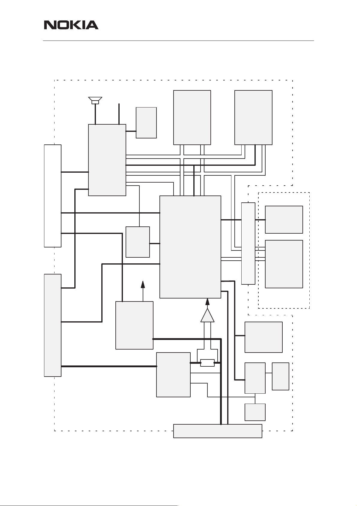
RF
Mod/IF
Audio
RF control
VRX, VTX
BUZZER
MASI
Audio/
Signalling
ASIC
XT AL
14..7456M
ADDRESS
CONTROL
DATA
SIS
VL VA
FLASH SRAM
512Kx16 64kx8
MCU
H8 2322
8k RAM
ROMless
8ADC ports
I/O ports
UI CONNECTOR
Serial ports
LCD
Keyboard
XMIC,XEAR,MIC
MBUS,FBUS
BOTTOM CONNECTOR
CHARGER
PSA
Power
Supply
ASIC
PWM outputs
CHAPS
0R22
Charger
ASIC
BATTERY CONNECTOR
Figure 1.
I2C
EEPROM
RTC
Back–up
Battery
XTAL
32.768k
Issue 3 02/2000
Nokia Mobile Phones Ltd.
Page 9
Page 10

THF-12
System Module NH1
Technical summary
The baseband module consists of Hitachi H8S processor 2322, four ASIC
circuits, PSA, CHAPS, MASI and SIS, and some standard circuits,
FLASH, SRAM, EEPROM and a RTC.
The MCU includes 8 kbytes RAM. It controls all transceiver functions.
FLASH size is 1Mbytes and SRAM 64kBytes
The EEPROM type is 16 kbytes with 32 bytes and it’s a serial I
type, RTC is connected to the same bus and SDAT line is also used to
control LCD.
The baseband is running from a 2.8 V power rail, which is supplied by a
power controlling asic. In the PSA asic there are two separate power sup-
plies for BaseBand ( VA,VL ) and two externally controllable power sup-
plies for RF (VRX, VTX).
PAMS Technical Documentation
2
C–bus
The CHAPS is a charging control ASIC. It is essentially
power switch for controlling charging current, in a mobile phone. CHAPS
is designed for 3 cell Nickel or 1 cell Lithium battery packs.
The MASI circuit integrates the Audio and Modem operations. It includes
audio power amplifier for EAR and XEAR lines. MASI includes also driver
for buzzer.
All functional blocks of the baseband are mounted on a single multi layer
printed circuit board. All components of the baseband are surface mount-
able. This board contains also the RF–parts. The B–cover side ( battery
side ) EMC shielding is implemented by using a metallized inside of
B–cover as a shield on the RF–blocks. On the other side the engine is
shielded with a aluminium frame, which makes a contact to a ground ring
of the engine board.
The connections from BaseBand to UI board are fed through a 28–way
2–row board to board spring connector.
Modes of Operation
Power off, Standby, Listening and Conversation modes.
– In Power off mode only the circuits needed for power up are supplied.
an integrated
Page 10
– In Standby mode the MCU and needed blocks of the MASI are active,
in SLEEP mode MASI cuts off system clock.
– In Listening mode the receiver and some blocks of the MASI are ac-
tive.
– In Conversation mode all ICs are active.
Nokia Mobile Phones Ltd.
Issue 3 02/2000
Page 11
PAMS Technical Documentation
Technical Specifications
Maximum Ratings
Parameter Rating
Battery voltage, idle mode 3.2... 5.3 V (5.0V in call mode)
Charger input voltage –5.0 ... 16V
Operating temperature range –25C to +55C
Storage temperature range –40C to +85 C
Charging of the batteries is possible only in the temperature range +5 ...
+45 °C.
DC Characteristics
THF-12
System Module NH1
Supply Voltage Lines and power consumption are listed in the table be-
low:
Line Symbol Minimum Typical /
Nominal
Supply battery voltage 3.2 3.6 4.5 (5.3 in
Battery cut off voltage (HW) 2.7 2.8 2.9 V (3.2V min SW
Regulated logic supply voltage (VL) 2.72 2.82 2.9 V
Regulated logic supply current 0 40 mA
Regulated audio supply voltage (VA) 2.7 2.8 2.85 V
Regulated audio supply current 0 100 mA
Regulated RX supply voltage (VRX) 2.7 2.8 2.85 V
Regulated RX supply current 0.05 50 mA
Regulated TX supply voltage (VTX) 2.7 2.8 2.85 V
Regulated TX supply current 0.02 60 mA
Current consumption standby mode 65 mA
Current consumption sleep mode 11 mA
Maximum Unit / Notes
V
idle mode)
cutoff)
Current consumption conv. low power 650 mA
Current consumption conv. high power 1100 mA
Issue 3 02/2000
Nokia Mobile Phones Ltd.
Page 11
Page 12
THF-12
System Module NH1
PAMS Technical Documentation
Battery connector
The electrical specifications for the battery connector:.
Pin Name Min Typ Max Unit Notes
1 BVOLT 3.2 3.6 4.5 V Battery voltage
5.3 Maximum voltage in idle state with charger
2 BSI
3 BTEMP
0 2.85 V Battery size indication
Phone has 100kohm pull up resistor.
2.2 18 kohm Battery indication resistor (Ni battery)
20 22 24 kohm Battery indication resistor (service battery)
27 51 kohm Battery indication resistor (4.1V Lithium
battery)
68 91 kohm Battery indication resistor (4.2V Lithium bat-
tery)
0 1.4 V Battery temperature indication
Phone has a 100k (+–5%) pullup resistor,
Battery package has a NTC pulldown resis-
tor:
47k+–5%@+25C , B=4050+–3%
20 22 25 kHz PWM control to VIBRA BATTERY
4 BGND 0 0 V Battery ground
UIF–connector
Signal Name Pin Notes
VL 1–2 Logic supply voltage 2.8V
ROW0,1,2 4–6 Lines for keyboard write
BACKLIGHT 22,23 Backlights supply
COL0–6 7–11,15,16 Lines for keyboard read
LCD_CLK 17 External LCD clock
LCD_SCLK 18 LCD Driver serialclock
LCD_SDAT 19 LCD Driver serialdata
LCD_CS 20 LCD Driver chipselect
LCD_DC 21 LCD Driver data/control select
LCD_RESET 22 LCD Driver reset
GND 25–28 Ground
Page 12
Nokia Mobile Phones Ltd.
Issue 3 02/2000
Page 13

PAMS Technical Documentation
CTRLU Circuit
Block Description
CTRLU – CONNECTORU
Between MCU and system connector all data lines are protected for ESD.
HEAD_DET, Headset detection
Headset is detected by voltage level in XMIC line, it goes to MCU A/D
converter. When headset is not connected HEAD_DET DC level is same
as VL because of pull up resistor. When headset is connected DC level
drops so that if can be detected. In talk mode mic bias current is fed to
headset with HEAD_BIAS control it also increases the voltage level in
XMIC line which must be noticed.
HOOK_DET, Hook detection
Hook in headset is detected with MCU input port. HOOK_DET line goes
low when button is pushed in headset.
THF-12
System Module NH1
CTRLU – PWRU
The MCU controls the watchdog timer in the PSA. It sends a positive
pulse at approximately 1 s interval to XPWROFF pin of the PSA to keep
the power on. If CTRLU fails to deliver this pulse, the PSA will remove
power from the system. CTRLU controls also the charger on/off switching
in the PWRU block. When power off is requested CTRLU leaves PSA
watchdog without reset. After the watchdog has elapsed PSA cuts off the
supply voltages from the phone. Battery charging is controlled by CSW
line.
VBATSW, Battery voltage measurement
Battery voltage can be measured up–to 6.2V with 2.8 V reference voltage. The absolute accuracy is low because of the reference 3 % accuracy and A/D–converter +/– 8 LSB accuracy . This battery voltage measurement must be calibrated with input voltage 4.1 V. The A/D conversion result can be calculated from this equation:
A/D readout = 1024 * (VBAT* ( 0.45)) / VREF VREF=2.8 V
For example:
4.1 V results =674
ICHARG, Charger current measurement
Charger current is calculated from the voltage difference of the ends of
the shunt resistor that the charging current goes thru. The difference of
these voltages are first amplified by factor of 6.8 with op–amp to get more
accuracy to the measurement measured from different ends of charging
current shunt resistor. The absolute accuracy is low because there is very
small change in voltages with different currents . The measurement error
is minimized with calibration of the A/D–converter with 0 A and 0.5 A
charging currents.
Issue 3 02/2000
Nokia Mobile Phones Ltd.
Page 13
Page 14

THF-12
System Module NH1
VCHARG , Charger voltage measurement
Charger voltage can be measured up to 16.8 V nominal. The A/D–conversion result can be calculated from equation :
A/D readout = 1024 * (VCHARG*(10/60)) / VREF
VREF=2.8 V
For example:
7.5 V gives 457
BSI, Battery size indication
The battery type can be defined with the BSI resistor value. Batteries
with different capacities and with different cell types can be defined individually, BSI is calibrated with service battery.
BTEMP, Battery temperature measurement
The battery temperature measurement is implemented with 47 kohm
NTC with N value of 4050 and 47 kohm pullup resistor. BTEMP is calibrated with service battery.
PAMS Technical Documentation
CTRLU – AUDIO
The interface between the MCU and the MASI circuit is a bidirectional
8–bit data bus with 5 address lines. MASI is connected to the same address bus as Flash and SRAM memories, MASI has own address space.
MASI has one separate control line XINT for interrupt output to MCU.
CTRLU – UIF
The keyboard is connected directly to the controller. Data lines 0–7 are
input lines and ROW0–2 are output lines. Normally all ROW lines are set
to ’0’ and if any key is pressed the KBINT line indicates it to MASI and
MASI gives an interrupt to MCU which the starts scanning the keys. The
scanning is done by driving one ROW line to 0 V at the time, then the
corresponding data line goes to 0V and phone knows which key is
pressed. ROW(0:2) lines must be in 0 V state when phone is in sleep
mode so that key pressing can be indicated.
Data to LCD Driver is written through a serial port which is used to control RTC and EEPROM too.
Keyboards and LCD lights are controlled by LIGHTS signal.
CTRLU – RX
The RX circuit power is connected on/off by the RXE signal.
Received signal strength is measured over the RSSI and intermediate fre-
quence is measured over the IF.
CTRLU – SYNT
RF temperature is measured over the RFTEMP. Frequency is controlled
by AFC signal. Synthesizer is controlled via synchronous serial bus
Page 14
Nokia Mobile Phones Ltd.
Issue 3 02/2000
Page 15
PAMS Technical Documentation
SDAT/SCLK. The data is latched to the synthesizer by the positive edge
of SLE line. TX synthesizer power on/off (TXS/port P3) line is controlled
via PLL circuit.
CTRLU – TX
Transmitter output power level is measured over the TXI. TXE line activates power module. The power is controlled via TXC line which is PWM–
controlled output port.
Main Components
MCU
MCU H8/2322 is a CMOS microcontroller. The CPU is ROMless so all
memory needed is located outside the chip.
MCU operating clock (=14.7456 MHz) is generated in the MASI.
THF-12
System Module NH1
Controller Ports
Pin no Symbol Description Pin type
1 Vcc
2–23 A0–A19 FLASH,MASI and RAM Address bus address
24 Ass
25 A20 NC I
26 PA5 NC I
27 PA6 NC I
28 PA7 NC I
29 P67 NC I
30 P66 HOOK_DET Handset HOOK signal I
31 P65 HEAD_BIAS Headset microphone bias control I/O
32 P64 XINT interrupt signal from MASI I/O
33 Vcc
34–37,
39–46,
48–51
D0–D15 Data bus Data
38,47 Vss
52 Vcc
53 P30/TxD0 MBUSTX I/O
54 P31/TxD1 LCD_SDAT, RTC_SDAT, EEPROM_SDAT I/O
55 P32/RxD0 MBUSRX I/O
56 P33/RxD1 VPPCON I/O
57 P34/SCK0 ROW1 I/O
Issue 3 02/2000
Nokia Mobile Phones Ltd.
Page 15
Page 16
THF-12
System Module NH1
PAMS Technical Documentation
58
59 Vss
60 P60/CS4/
61 P61/CS5/
62 P62/_DREQ1ECLK serial clock (EEPROM, RTC) I/O
63 P63/_TEND1LIGHTS I/O
64 P27 SLE I/O
65 P26 ROW0 I/O
66 P25 MBUSRX timer I/O
67 P24 SCLK serial clock for SYNT I/O
68 P23 SIS_SDAT I/O
69 P22 TXE I/O
70 P21 SIS RESET I/O
P35/SCk1 LCD_SCLK I/O
NC I
_DREQ0
NC I
_TEND0
71 P20 RXE I/O
72 _WDTOVF–
73 _RES XRES reset for MCU, FLASH, MASI from PSA
74 NMI –
75 _STBY –
76 Vcc
77 XTAL –
78 EXTAL CLKMCU from MASI
79 Vss
80 PF7 PWRON I
81 Vcc
82 _AS –
83 _RD FLASH,MASI,RAM Read
84 _HWR MASI, RAM Write
85 _LWR FLASH Write
86 PF2 LCD_CS I/O
87 PF1 LCD_DC I/O
88 PF0 LCD_RESET I/O
89 P50/TxD2 FBUSTX / BOOST0 I/O
90 P51/RxD2 FBUSRX / BOOST1 I/O
Page 16
Nokia Mobile Phones Ltd.
Issue 3 02/2000
Page 17
THF-12
PAMS Technical Documentation
91 * P52/SCK2 MBUS RX used for FBUS CLK I/O
92 P53 SIS SCLK I/O
93 AVcc
94 Vref
95 AN0 VBATSW Analog
96 AN1 VCHARG Analog
97 AN2 RSSI Analog
98 AN3 ICHARG Analog
99 AN4 BTEMP Analog
100 AN5 BSI Analog
101 AN6 RFTEMP Analog
102 AN7 HEAD_DET Analog
103 AVss
System Module NH1
104 Vss
105 P17 LIM I/O
106 P16 TXC I/O
107 P15 CDET I/O
108 P14 CSW I/O
109 P13 XPWROFF I/O
110 P12 FM–ENABLE I/O
111 P11 SYNTH SDAT I/O
112 P10 VIBRA I/O
113 MD0 0
114 MD1 0
115 MD2 1
116 PG0 ROW2 I
117 PG1 NC I
118 PG2 RAMCS I
119 PG2 MASICS I
120 PG2 FLASHCS I
– FLASH memory 1Mx16 with 16 bit databus
– SRAM memory 16kx8 with 8 bit databus
Issue 3 02/2000
Nokia Mobile Phones Ltd.
Page 17
Page 18
THF-12
System Module NH1
SIS
AT90S2343 is the SIS (subscriber identification) circuit connected to the
controller over serial bus IIC..
Table 1. SIS–prosessor signals:
Pin Description
EXTAL Clock input from MASI
RESET Reset input
PD0 IIC bus data
PD1 IIC bus clock
EEPROM
There is one 16k EEPROMs in phone. EEPROM is a nonvolatile memory
into which is stored the tuning data for the phone. In addition, it contains
the short code memory locations to retain user selectable phone numbers. SDAT line is used for control LCD and RTC too.
PAMS Technical Documentation
Pin Description
SDA IIC bus data
SCL IIC bus clock
RTC
The real time clock is connected to the same IIC bus as the EEPROM.
RTC alarm interrupt is connected to the XPRWON line, so it works even if
phone is powered off. Backup power supply to the RTC is done with a
separate battery which is charged through the CHAPS.
Page 18
Nokia Mobile Phones Ltd.
Issue 3 02/2000
Page 19

PAMS Technical Documentation
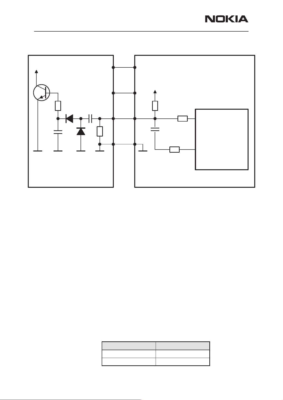
PWRU
Power Distribution
The main components of the Power Unit are the PSA ( Power Supply
Asic) and the CHAPS ( Charger Power Switch ).
In normal operation the baseband is powered from the phone‘s battery.
The battery consists of three Nickel Metal Hydride cells. There is also a
possibility to use batteries consisting of one Lithium–Ion cell. An external
charger is used for recharging the battery and supplying power to the
phone. The charger can be either a standard charger that can deliver
around 400 mA or a so called performance charger, which can deliver
supply current up to 850 mA.
The baseband contains components that control the power distribution to
the whole phone excluding those parts that use continuous battery supply. The battery feeds power directly to three parts of the system: PSA,
RF–power amplifier, and UI (buzzer and display and keyboard lights).
THF-12
System Module NH1
The power management circuit CHAPS provides protection against overvoltages, charger failures and pirate chargers etc. that could otherwise
cause damage to the phone.
Battery charging
Acceptable chargers are detected by the software. The absolute maximum input voltage is 30V due to the transient suppressor that is protecting the charger input. At the phone end there is no difference between a
plug–in charger or a desktop charger. The DC–jack pins and bottom connector charging pads are connected together inside the phone. The
charging block diagram is below.
Issue 3 02/2000
Nokia Mobile Phones Ltd.
Page 19
Page 20
THF-12
System Module NH1
PAMS Technical Documentation
LIM
CSW
MCU
MCU
0R22
VBAT
VBATSW
VCHARGSW
PSA
GND
VCHAR
LIM
VOUT
RSENSE
PWM
10k
22p
CHAPS
VCH
GND
TRANSCEIVER
1u
50.3k
10k
10k
Figure 2. Charging block diagram
30V
2A
VIN
CHRG_CTRL
L_GND
CHARGER
NOT IN
ACP–7
Startup charging
When a charger is connected, the CHAPS is supplying a startup current
minimum of 130mA to the phone. The startup current provides initial
charging to a phone with an empty battery. The startup circuit charges
the battery until the battery voltage level reaches 3.0V (+/– 0.1V) and the
PSA releases the PURX reset signal and program execution starts.
Charging mode is changed from startup charging to PWM charging that is
controlled by the MCU software. If the battery voltage reaches 3.55V
(3.75V maximum) before the program has taken control over the charging, the startup current is switched off. The startup current is switched on
again when the battery voltage has decreased to 100mV (nominal).
Table 2. Startup characteristics
Parameter Symbol Min Typ Max Unit
VOUT Start– up mode cutoff limit Vstart 3.45 3.55 3.75 V
VOUT Start– up mode hysteresis
NOTE: Cout = 4.7 uF
Start–up regulator output current
VOUT = 0V ... Vstart
Vstarthys 80 100 200 mV
Istart 130 165 200 mA
Battery overvoltage protection
Output overvoltage protection is used to protect phone from damage.
This function is also used to define the protection cutoff voltage for differ-
Page 20
Nokia Mobile Phones Ltd.
Issue 3 02/2000
Page 21
PAMS Technical Documentation
ent battery types (Li or Ni). The power switch is immediately turned OFF if
the voltage in VOUT rises above the selected limit VLIM1 or VLIM2.
Table 3. VLIM characteristics
Parameter Symbol LIM input Min Typ Max Unit
THF-12
System Module NH1
Output voltage cutoff limit (during transmission or Li–battery)
Output voltage cutoff limit (no
transmission or Ni–battery)
The voltage limit (VLIM1 or VLIM2) is selected by logic LOW or logic
HIGH on the CHAPS (N101) LIM– input pin. Default value is lower limit
VLIM1.
When the switch in output overvoltage situation has once turned OFF, it
stays OFF until the the battery voltage falls below VLIM1 (or VLIM2) and
PWM = LOW is detected. The switch can be turned on again by setting
PWM = HIGH.
VCH
VCH<VOUT
VOUT
VLIM1 or VLIM2
VLIM1 LOW 4.4 4.6 4.8 V
VLIM2 HIGH 4.8 5.0 5.2 V
t
SWITCH
PWM (32Hz)
ON OFF
Figure above: Battery overvoltage protection
Battery removal during charging
Output overvoltage protection is also needed in case the main battery is
removed when a charger connected or a charger is connected before the
battery is connected to the phone.
With a charger connected, if VOUT exceeds VLIM1 (or VLIM2), the
CHAPS turns switch OFF until the charger input has decreased below
Issue 3 02/2000
Nokia Mobile Phones Ltd.
t
ON
Page 21
Page 22
THF-12
System Module NH1
Vpor (nominal 3.0V, maximum 3.4V). The MCU software stops the charging (turn off PWM) when it detects that the battery has been removed.
The CHAPS remains in protection state as long as the PWM stays HIGH
after the output overvoltage situation has occurred.
PAMS Technical Documentation
VCH
(Standard
Charger)
VOUT
PWM
SWITCH
Vpor
VLIM
4V
Vstart
”1”
”0”
ON
OFF
Droop depends on load
& C in phone
2
5
4
6
7
Istart off due to VCH<Vpor
Vstarthys
t
t
t
1.1Battery removed, (standard) charger connected, VOUT rises (follows charger voltage)
2. VOUT exceeds limit VLIM(X), switch is turned immediately OFF
3.3VOUT falls (because no battery) , also VCH<Vpor (standard chargers full–rectified
output). When VCH > Vpor and VOUT < VLIM(X) –> switch turned on again (also PWM
is still HIGH) and VOUT again exceeds VLIM(X).
4. Software sets PWM = LOW –> CHAPS does not enter PWM mode
5. PWM low –> Startup mode, startup current flows until Vstart limit reached
6. VOUT exceeds limit Vstart, Istart is turned off
7. VCH falls below Vpor
Figure above: Battery removal during charging
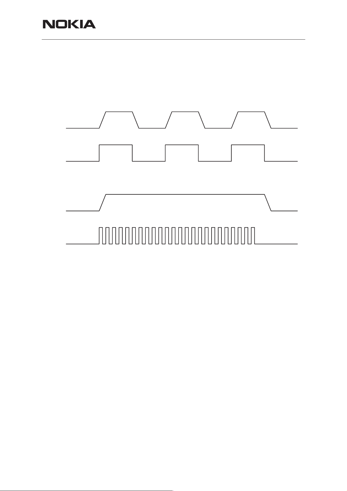
Different PWM frequencies ( 1Hz and 32 Hz)
When a travel charger (2– wire charger) is used, the power switch is
turned ON and OFF by the PWM input when the PWM rate is 1Hz. When
the PWM is HIGH, the switch is ON and the output current Iout = charger
current – CHAPS supply current. When PWM is LOW, the switch is OFF
and the output current Iout = 0. To prevent the switching transients inducing noise in audio circuitry of the phone soft switching is used.
Page 22
Nokia Mobile Phones Ltd.
Issue 3 02/2000
Page 23
PAMS Technical Documentation
The performance travel charger (3– wire charger) is controlled with PWM
at a frequency of 32Hz. When the PWM rate is 32Hz CHAPS keeps the
power switch continuously in the ON state.
THF-12
System Module NH1
SWITCH
ON ONON OFF OFF
PWM (1Hz)
SWITCH
ON
PWM (32Hz)
Figure 3. Switch control with 2Hz and 32 Hz frequencies (in this case 50% duty cycle)
Issue 3 02/2000
Nokia Mobile Phones Ltd.
Page 23
Page 24
THF-12
System Module NH1
PAMS Technical Documentation
Vibra
22k
100n
BATTERY
10n
VBAT
BSI
BTEMP
R
T
47k
NTC
GND
Figure 4. Vibra battery
TRANSCEIVER
VA
100k
10k
BTEMP
10n
MCU
10k
VIBRAPWM
Supply voltage regulators and controlling
The heart of the power distribution is the PSA asic. It includes all the voltage regulators and feeds power to the whole system. The baseband digital and analog parts are powered from the VL and VA regulators which
provide the 2.82 V baseband supply. The baseband regulators are active
when the phone is powered on.
The PSA includes also two 2.82 V regulators (VRX and VTX) providing
power to the RF section. These regulators can be controlled by the direct
control signals from the MCU. The VRX regulator can also be controlled
by the signal from the NASTA.
– VTX_ENA ( from MCU ) controls VTX regulator
– PSBS_ENA ( from NASTA ) controls VRX regulator
In addition PSA includes also functions listed bellow:
– Buffer for the M2BUS.
The buffer translates the logical input signal to open–drain output.
Table 4. M2BUS buffer truth table
Input Output
Page 24
LOW LOW
HIGH Z
Nokia Mobile Phones Ltd.
Issue 3 02/2000
Page 25
PAMS Technical Documentation
– Power on/off and reset logic. The Power off logic can be used as a
watchdog.
– Supply voltage monitor and automatic reset/power–off.
VBATSW is internally divided and buffered battery voltage output. The
A/D –converter input monitoring the battery voltage can be connected
here. The circuit monitors the voltage at the VBAT input and forces
the circuit to Reset if the voltage level is below allowed limit voltage,
VBATcoff–. A hysteresis is included to prevent oscillation between different states.
– Battery charger detection.
Externally divided charger voltage VCHAR goes through PSA internal
switch to VCHARSW output. The A/D –converter input monitoring the
charger voltage can be connected here.
– Automatic on–chip current limiting
– On–chip thermal shutdown, which protects PSA from overheating.
Thermal shutdown includes hysteresis in order to prevent oscillation
during the thermal protection.
THF-12
System Module NH1
Table 5. Regulators VA and VL characteristics
Parameter
Test Conditions
Output Voltage VL, VA 2.73
Output current of the regulator
(all regulators enabled)
Quiescent current
VL: Iload = 0mA
Iload = 40mA
VA: Iload = 0mA
Iload = 100mA
Quiescent current
Tamb = +25_C, VBAT=3.6V
VL: Iload = 0mA
Iload = 40mA
VA: Iload = 0mA
Iload = 100mA
Quiescent current in Power–Off
VL
VA
Line regulation: VL, VA
IoutVL = 40mA,
IoutVL = 100mA,
3.25VVBAT5.2V
Symbol Limits
Min Typ Max
Iout
Iout
Iq
Iq
Iqoff
VL
VL
VA
line
, VA
line
040
0 100
2.82
110
130
110
130
Unit
2.90
mA
mA
200
220
200
220
6
15
20 mV
A
A
A
A
A
A
A
A
A
A
V
Load regulation: VL, VA
0mAIloadVL40mA,
0mAIloadVA100mA,
3.25VVBAT5.2V
Issue 3 02/2000
VL
, VA
load
load
E Nokia Mobile Phones Ltd.
30 mV
Page 25
Page 26
THF-12
System Module NH1
Table 5. Regulators VA and VL characteristics (continued)
PAMS Technical Documentation
Test Conditions
Line transient:
AC=0.5V square wave
Slew rate = 50 mV/s
f = 500Hz ... 2kHz
3.5VVBAT5.2V
Load transient: VL, VA
IloadVL 100A to 40mA,
Iload
10s
3.25VVBAT5.2V
Current limit (VL,VA = 0V)
VL
VA
Power Supply Ripple Rejection
0mAIloadVA100mA
Settling time
Cload=1F20%
load current 0mA
100A to 100mA in
VA
3.2VVBAT5.2V
0mAIloadVL40mA,
f = 10Hz ... 10kHz
SymbolParameter
VL
linet
V
Trec
Note 1
I
lim
Min Typ Max
r, VA
linetr
PSRR 40 dB
ts
Note 2
40 dB
40
20
60 180
150 450
160 s
UnitLimits
mV
s
mA
mA
Note 1: Voltage deviation (V) is the output voltage overshoot in tran-
sient response. Recovery time (Trec) is the time from the beginning of the
transient response to the time point when the regulator output voltage first
crosses the final stable value after overshoot.
Note 2: Settling time is defined from the time point of mode change Power–Off to Reset to the time when regulator output voltage is within 5% of
the final value.
Table 6. Regulators VRX and VTX characteristics
Parameter
Test Conditions
Output Voltage VRX, VTX 2.73
Output currents of the regulators
(all regulators enabled)
Quiescent current
VRX: Iload = 0A
Iload = 50mA
VTX: Iload = 0A
Iload = 60mA
Symbol Limits
Min Typ Max
Iout
Iout
Iq
VRX
VTX
0.05 50
0.02 60
2.82
2.90
320
360
320
360
Unit
V
mA
mA
A
A
A
A
Page 26
Nokia Mobile Phones Ltd.
Issue 3 02/2000
Page 27
PAMS Technical Documentation
Table 6. Regulators VRX and VTX characteristics (continued)
THF-12
System Module NH1
Test Conditions
Quiescent current
Tamb = +25_C, VBAT=3.6V
VRX: Iload = 0A
Iload = 50mA
VTX: Iload = 0A
Iload = 60mA
Quiescent current in Power–Off
VRX
VTX
Line regulation: VRX, VTX
IoutVRX = 50mA,
IoutVTX = 60mA,
3.25VVBAT5.2V
Load regulation: VRX, VTX
50AIload
20AIload
VRX
VTX
50mA,
60mA,
3.25VVBAT5.2V
Line transient: VRX, VTX
AC=0.5Vpp square wave
Slew rate = 50 mV/s
f = 500Hz .... 2kHz
3.5VVBAT5.2V
Load transient: VRX, VTX
Iload
50A to 50mA,
VRX
IloadVTX 20A to 60mA in 10s
3.25VVBAT5.2V
SymbolParameter
Iq
Iqoff
VRX
line,
VRX
load,
VRX
linetr,
V
Trec
Note 1
VTX
VTX
VTX
line
load
linetr
UnitLimits
Min Typ Max
180
195
180
195
14
17
A
A
A
A
A
A
20 mV
30 mV
40 dB
40
20
mV
s
Current limit (VRX,VTX = 0V)
VRX
VTX
Power supply ripple rejection
3.25VVBAT5.2V
50AIload
20AIload
VRX
VTX
50mA,
60mA,
f = 10Hz.....10kHz
f = 10Hz.....50kHz
f = 10Hz.....100kHz
Settling time,
Cload=1F20%
load current 0mA
Note 1: Voltage deviation (V) is the output voltage overshoot in tran-
sient response. Recovery time (Trec) is the time from the beginning of the
transient response to the time point when the regulator output voltage first
crosses the final stable value after overshoot.
Note 2: Settling time is defined from VTX_ENA/VRX_ENA rise to the time
when regulator output voltage is within 5% of the final value.
I
lim
PSRR
VRX,VTX
ts
Note 2
75 225
90 270
50
40
35
100 s
mA
mA
dB
dB
dB
Issue 3 02/2000
E Nokia Mobile Phones Ltd.
Page 27
Page 28

THF-12
O
System Module NH1
Operation modes
The circuit has three operational modes: Power–Off, Reset and Power–
On. The additional modes are the Protection mode and Battery disconnected (VBAT < VRth, master reset threshold). Respective conditions of
the external signals are described in Table 7.
PAMS Technical Documentation
Table 7. Operational modes
MODE PURX VRX_ENAVTX_ENAVLVAVRX VTX VBATSW VCHAR
–SW
Power–
Off
Reset
Power–
n
LOW X X Z Z Z Z Z LOW
LOW L L 2.8V Z Z Z Z LOW
LOW H H 2.8V 2.8V 2.8V Z Z LOW
HIGH
L L 2.8V Z Z VBATSW VCHAR XPWRONX
H H 2.8V 2.8V 2.8V VBATSW VCHAR XPWRONX
NOTE: VBATSW and VCHARSW are controlled by internal VSW_ENA–
signal during power–on.
NOTE: PWRONBUFF is an inverted (and buffered) PWRONX. A logic
LOW level at PWRONX (active LOW) will force a logic HIGH level at
PWRONBUFF.
Power–Off Mode
In order to be in Power–Off mode VBAT must be above VRth.
During Power–Off mode PURX is at logical low level. VA, VL, VRX and
VTX regulators are disabled and in high–Z low output state.
PWRON-
BUFF
Entering Power–Off Mode
The PSA contains a watchdog counter that is reset by writing ”1” – ”0” sequence to input PWROFFX.
The circuit goes to Power–off mode from Power–On after delay Toff if
watchdog has not been reset during this time.
The other possibility to enter the Power–Off is from Reset, if the PSA can
not enter Power–On mode because VBATcoff+ is not reached. This
means that watchdog elapses before the microcontroller is able to produce a pulse to PWROFFX. If charger is present (VCHAR>VCHARth),
transition from Reset to Power–Off can not occur but the circuit stays in
Reset mode as long as battery has been charged above VBATcoff+.
The circuit goes to battery disconnected mode if battery voltage drops below master reset threshold (VRth–).
For testing purposes the watchdog can be disabled and reset by grounding the WD_DISX pin. In normal use it can be left floating (internal pull
up).
Page 28
Nokia Mobile Phones Ltd.
Issue 3 02/2000
Page 29

PAMS Technical Documentation
Charging in Power–Off
Charging is not possible in Power–Off. Connecting a charger during Power–Off generates a rising edge on VCHAR input and the circuit enters Reset mode. Circuit stays in Reset as long as the battery is charged to the
limit VBATcoff+.
If the watchdog elapses during Power–On when charger is connected,
the circuit goes to Power–Off. Because charger detection is level sensitive, charger is detected and the circuit goes via Reset mode to Power–
On mode.
Reset Mode
The circuit goes into Reset mode from Power–Off when:
– the battery voltage is initiated (master reset) or
– logic low voltage in PWRONX is detected or
THF-12
System Module NH1
– charger voltage becomes available or
– when recovering from Protection mode
In Reset mode the VL and VA outputs are activated by an internal enable
signal. The VRX and VTX have external enable inputs VRX_ENA and
VTX_ENA. VBATSW and VCHARSW are disabled and PURX is LOW.
The circuit leaves the Reset mode after a delay Trd for Power–On if VBAT
> VBATcoff+. Watchdog is reset when Power–On mode is entered.
The circuit goes into Reset mode from Power–On when the battery voltage VBAT drops below VBATcoff–.
VBAT is monitored internally, hence if voltage VBAT drops below the
threshold (determined by internal resistors), transition from Power–on to
Reset mode is done. If VBAT doesn’t rise back above reset release limit
in time T
the Watchdog elapses and the circuit powers off.
off
To avoid PSA going to RESET mode due to fast transient, transition from
Power–On to Reset mode is not done if VBAT is below VBATcoff– for
shorter time than threshold detection delay T
dd.
The circuit leaves the Reset mode after a delay Trd if VBAT > VBATcoff+.
Issue 3 02/2000
Nokia Mobile Phones Ltd.
Page 29
Page 30

THF-12
System Module NH1
VBAT
VBATcoff +
VBATcoff
VBATcoff –
PURX
PAMS Technical Documentation
T>TddT<Tdd
Tdd Trr
Figure 5. Threshold detection delay Tdd and PURX reaction time T
Power–On Mode
In Power–on mode all the functions are active. VBATSW and VCHARSW
outputs are activated by the internal enable signal VSW_ENA. PURX is
high in Power–On.
From Power–On mode the circuit goes to Power–Off mode after a delay
Toff (watchdog delay set by an external capacitor Cosc) if no writing sequence to PWROFFX from logical high level to low level has detected
during this time.
In Power_on mode the circuit does not react on PWRONX pulse i.e.
the circuit must be switched off by the system by not updating the watchdog writing in time Toff.
rr
Page 30
Nokia Mobile Phones Ltd.
Issue 3 02/2000
Page 31

PAMS Technical Documentation
AUDIO BLOCK
The Audio Block comprises the MASI, which is is a single chip audio/signalling processor in a 64 TQFP package for NMT450 system
Main features
– Low power consumption modes
– 8 bit parallel interface with pull ups
– FM demodulator
FFSK modem features
– Full duplex 1200 baud signalling
– FSK indicator and level detector
– FII filter and gain control
– DMS facility
THF-12
System Module NH1
Audio features
– Low noise microphone amplifier
– Input for a handset microphone or an accessory
– Microphone sensitivity compensation +24/–7 dB range (5 bits)
– Compander
– RX and TX filters
– Tx hard limiter
– Tx AGC
– Transmitter compensation amplifier with +1.875/–1.875 dB range (4
bits)
– Compensation amplifier for different RX deviations with +7.5/0 dB
range (4 bits)
– Volume control amplifier with –20/+17.5 range (4 bits)
– Earphone amplifier with drive capability for ceramic earpiece
– Buffered output for a handset or an accessory
– Mute switches
– Speech scrambler and descrambler
– Hands free functions
Other features
– Driver for buzzer
– Call continue sensor
– Negative supply voltage for LCD
– Dual and single tone multifrequency generator
– IF counter
– 8 bit general purpose DAC
– Programmable output clocks with clock stop for MCU, LCD and SIS
– Two external interrupt sources
– Programmable timer
– Summing stage for voice/data, signalling and fii
– FM radio
Issue 3 02/2000
Nokia Mobile Phones Ltd.
Page 31
Page 32

THF-12
System Module NH1
PAMS Technical Documentation
Technical specifications
Table 8. AUDIO internal Signals, Inputs
Signal Name Notes From
VBAT Battery voltage PWRU
VA Analog supply voltage, 2.8V PWRU
XRES Reset line from PSA PWRU
XMRD Read control signal CTRLU
XMCS Chip select signal CTRLU
XMWR Write control signal CTRLU
MA0...A4 5–bit address bus CTRLU
MD0...D7 8–bit bidirectional data bus CTRLU
KBINT Keyboard interrupt CTRLU
MBUSINT MBUS interrupt CTRLU
HEAD_BIAS Headset microphone bias enable CTRLU
IF (2nd) Intermediate frequency for MASI RX
XMIC External audio input from accessories SYSTEM
MICP Microphone (positive node) SYSTEM
MICN Microphone (negative node) SYSTEM
FM_ENABLE FM radio enable CTRLU
FM_ANTENNA FM–Antenna connection SYSTEM
FMCTRL FM–VCO control voltage SYNT
Table 9. AUDIO internal Signals, Outputs
Signal Name Notes To
XEAR External audio output to accessories SYSTEM
ACCDET Accessory detection signal SYSTEM
MOD Audio output to synthesizer SYNT
AFC VCTCXO control SYNT
BUZZER Buzzer signal SYSTEM
EARP Earpiece (positive node) UIF
EARN Earpiece (negative node) UIF
CLKSIS Clock signal for SIS CTRLU
CLKLCD Clock signal for LCD UIF
CLKMCU Clock signal for MCU CTRLU
XINT Interrupt request to MCU CTRLU
FMLOS FM–VCO frequency sample SYNT
Page 32
Nokia Mobile Phones Ltd.
Issue 3 02/2000
Page 33

PAMS Technical Documentation
Table 10. Pin list of MASI
Pin no Symbol Pin type Notes
1 VDD1 PWR +2.7 ... 3.5 V Supply voltage for digital part
2 XCS DIN/pd Chip select signal, active state LOW, pull–down > 50 kW
3 A4 DIN/pu 5–bit address bus, MSB, pull–up > 50 kW
4 A3 DIN/pu 5–bit address bus, pull–up > 50 kW
5 A2 DIN/pu 5–bit address bus, pull–up > 50 kW
6 A1 DIN/pu 5–bit address bus, pull–up > 50 kW
7 A0 DIN/pu 5–bit address bus, LSB, pull–up > 50 kW
8 D7 DIO 8–bit bidirectional data bus MSB
9 D6 DIO 8–bit bidirectional data bus
System Module NH1
THF-12
10 D5 DIO 8–bit bidirectional data bus
11 D4 DIO 8–bit bidirectional data bus
12 D3 DIO 8–bit bidirectional data bus
13 D2 DIO 8–bit bidirectional data bus
14 D1 DIO 8–bit bidirectional data bus
15 D0 DIO 8–bit bidirectional data bus LSB
16 NMI DOUT Non maskable Interrupt request
17 VSS1 PWR 0 V Supply voltage, ground for digital part
18 XCLR DIN HW reset input, active state LOW
19 TMODE DIN/pd Test mode selection, pull–down > 50 kW
20 TSEL DIN/pd Scan test selection, pull–down > 50 kW
21 XINT DOUT Interrupt request to MCU, active state LOW
22 EXTINT1 DIN External interrupt request, falling edge active (note: this pin
is test scan select when TMODE is high)
23 EXTINT2 DIN External interrupt request, falling edge active
24 VDD2 PWR +2.7 ... 3.5 V Supply voltage for digital in Analog part
25 IF AIN IF input
26 DAF AIN Audio input
27 FILO AOUT Rxfilter output
28 EXPI AIN Expander/Descrambler input
29 EXPO AOUT Expander/Descrambler output
30 VOLI AIN Volume control amplifier input
31 VSA1 PWR 0 V Supply voltage, ground for RX Analog
(including EARAMP & EXTEAR)
32 EXTEAR AOUT Buffered output for handset or an accessory
33 EARP AOUT Earphone driver output, positive
Issue 3 02/2000
Nokia Mobile Phones Ltd.
Page 33
Page 34

THF-12
System Module NH1
Table 10. Pin list of MASI (continued)
NotesPin typeSymbolPin no
34 VDA1 PWR + 2.7 ... 3.5 V Supply voltage for RX Analog
(including EARAMP & EXTEAR)
35 EARN AOUT Earphone driver output, negative
36 DACO AOUT DA converter output
37 CALLCNT AIN Voltage sensor input for battery change during call
38 REF AOUT Internal analog signal ground, stabilization capasitor
39 ATOUT AOUT Analog test circuit output
40 MIC AIN Microphone amplifier input,
41 BIMIC AOUT Microphone bias output
42 CMIC AIN Microphone bias current stabilizing capasitor
43 EXTMIC AIN Audio input for a handset or an accessory
PAMS Technical Documentation
44 TXPBO AOUT Transmit bandpass filter (scrambler) output
45 COMI AIN Compressor input
46 MOD AOUT transmit path output
47 ATST AOUT Analog test output
48 VDA2 PWR + 2.7 ... 3.5 V Supply voltage for TX Analog & NVSGEN
49 NSV AOUT Negative supply voltage, –7V output
50 NSV2 AOUT negative supply voltage –4.66V, for external capacitor
51 NSV1 AOUT negative supply voltage –2.33V, for external capacitor
52 NCPP AOUT Negative supply charge pump (external) capacitor positive
53 NCPN AOUT Negative supply charge pump (external) capacitor negative
54 VSA2 PWR 0 V Supply voltage, ground for TX Analog & NVSGEN
55 TOUT DOUT Test scan data output
56 CLKIN CIN 14.7456 MHz crystal oscillator input or input for the external
clock
57 CLKOUT COUT 14.7456 MHz crystal oscillator output
58 VSS2 PWR 0 V Supply voltage,
ground for digital in Analog part & Buzzer
59 BUZZ AOUT Buzzer output, open collector
60 CLKLCD DOUT Clock signal for LCD, 230.4 kHz, 57.6 kHz or 14.4 kHz
61 CLKSIS DOUT Clock signal for SIS processor, 3.6864MHz or 7.3728MHz
62 CLKMCU DOUT Clock signal for MCU, 3.6864 MHz, 7.3728 MHz or 14.7456
MHz
63 XWR DIN/pu Write control signal, active state LOW, pull–up > 50 kW
64 XRD DIN/pd Read control signal, active state LOW, pull–down > 50 kW
Page 34
Nokia Mobile Phones Ltd.
Issue 3 02/2000
Page 35

PAMS Technical Documentation
Receive (RX) Audio Signal Path
The incoming IF signal is first FM demodulated and then connected to RX
trimmer to compensate variation of nominal frequency deviation in different systems.
Receiving Data Path
The data from RX trimmer is filtered in the modems RX filter (MODRXFIL)
which includes de–emphasis function and from there to FSK discriminator. Further from FSK discriminator data is connected to detecting filter
(DETFIL) and from there to digital phase locked loop (DPLL).
Functional blocks of data reception path:
– FM demodulator
– RX trimmer
– De–emphasis filter
– Modems RX filter
– FSK indicator
– FSK level detector
– FSK discriminator
– Detecting filter
– Digital phase locked loop
– Reception controller
– Receivers register
THF-12
System Module NH1
Receiving Audio Path
FM demodulated audio signal is connected to the mux (RXMUX). There is
also possibility to select three other signals in the RXMUX (DTMF, rx mute
or audio test loop). Rx audio signal is 1:2 expanded and filtered in bandpass filter (RXFIL). Rx volume level is controlled with amplifier (VOL) in
the range –20 ... +17.5 dB.
If scrambling is in use signal is first expanded and then pre–emphased.
Pre–emphased signal is the descrambled and de–emphased.
Hands free control block (HFCONTR) includes a bandpass filter, window
comparator and controller for rx and tx attenuators. Rx hands free attenuator (RXATT) has selectable minimum gain from –30 ... –21 dB to max 0
dB. Rx and tx attenuation sum is always constant at hf use (–30 ... –21
dB).
There is also an extra filter (EARSFIL) for people who has a hearing defect. This filter emphases frequencies which are most sensitive in human
ear. Frequency response is +6 dB/oct from 0 to 1300 Hz and –3 dB from
1300 to 3400 Hz. This filter can be enabled by a control bit.
Normally signal is going to earphone amplifier (EAR). Signal is also available at the output of accessory buffer (ACC).
Functional blocks of audio rx path:
Issue 3 02/2000
Nokia Mobile Phones Ltd.
Page 35
Page 36

THF-12
System Module NH1
– FM demodulator
– RX trimmer
– RX mux
– De–emphasis filter
– Expander
– RX filter
– De–scrambler (in conjugation with extra pre–emphasis and de–em-
phasis)
– RX automatic gain control
– Ear sensitive filter
– Volume control
– Earphone and accessory buffers
RX Trimmer
Rx trimmer range is 0 .. +7 dB and step 0.5 dB.
Antialias filter is a lowpass filter which attenuates high frequency noise
before switched filters (fiifil, modrxfil and rxfil). It’s nominal gain is 0 dB.
PAMS Technical Documentation
Mux and de–emphasis
The input source (DTMF, DAF, ALOOP or mute) selects the input source
by bits RXSRCE(1:0) in register ACRB.
De–emphasis filter’s response is –6 dB/oct between 300 ... 3000 Hz. De–
emphasis is bypassed when BPEMP in ARCA is high and gain is then 0
dB.
Expander
Expander’s ratio is 1:2 in desibel scale. It is expanding dynamic of compressed speech back to normal. Gain in expander is min –24 ... +10 dB.
Expander’s attack time is 4 ms and decay time 9 ms. It can be bypassed
by bit BPEXP in reg ACRA. Bypass gain is +3 dB. Unaffected level is 100
mV (100 mV in gives 100 mV out). Expander can be set to work as compressor by bit RXCOMPEN in reg ACRA.
RX filter
Passband of rx bandpass filter is 300 ... 3000 Hz for speech.
De–scrambler
De–scrambler splits audio band into upper and lower frequency bands,
inverts both bands and sums them for clear signal. Possible splitting frequencies are 1130 Hz, 1380 Hz, 1600 Hz and 2140 Hz. De–scrambling
can be enabled and splitting frequency selected in register ACRI.
RX automatic gain control
The function of RXAGC is to keep level of received signal below specified
reference value.
Page 36
Nokia Mobile Phones Ltd.
Issue 3 02/2000
Page 37

PAMS Technical Documentation
Ear sensitive filter
Bandpasses speech spectrum taking attention to sensitivity of ear.
Volume control
Volume is controlled with an adjustable gain amplifier. Range is –20 ...
+17.5 dB and step is 2.5 dB (16 levels). Level is selected by bits VOL(3:0)
in register ACRB.
Earphone and accessory buffers
Earphone buffer is a differential amplifier. It is capable of driving 26 ohm
dynamic earphone. Earphone buffer is enabled by bit ACTEARP in register ACRB.
Accessory buffer is for accessory cable driving. It can be enabled by bit
ACTACC in register ACRB.
THF-12
System Module NH1
Transmitting paths
Transmitting data path
The data to be transmitted will be loaded into the transmitting register
TRREG. From the TRREG register the 8 bit data is transformed to serial
data which is sent to the FSK modulator (FSKMOD) and then to the summing block (SUM).
Functional blocks in data transmission path:
– Transmission controller
– Transmitters register
– FSK modulator with pre–emphasis
Transmitting audio path
Microphone signal is fed to microphone amplifier (MICAM). Signal source
is selected with a mux (TXMUX). Possible sources are own mic, accessories or DTMF generator. Tx hands free attenuator (TXATT) has selectable
minimum gain from –30 ... –21 dB. The maximum gain is 0 dB. In mictrimmer (MICTRI) signal from different sources is tuned for nominal deviation.
After the bandpass filter (TXBP) signal and 2:1 compressed in amplitude
compressor (COMPR) and then pre–emphasised +6dB/oct (PREEM).
Maximum level is set in AGC and limitter (LIM) blocks. Signal from LIM
block is lowpass filtered (TXLP) and fed to trimmer for speech maximum
deviation tuning. Output signal from TXLP is added to data and fii signals
in SUM block..
If scrambling is in use signal is first emphased and then scrambled and
de–emphased. Scrambled signal is then compressed and emphased
once more.
DTMF generator (DTMFGEN) generates dual and single tones for rx and
tx lines. Tolerance of DTMF frequencies is +–1.0 %.
Issue 3 02/2000
Nokia Mobile Phones Ltd.
Page 37
Page 38

THF-12
System Module NH1
Functional blocks of audio tx path:
– Mic amplifier and mux
– Mic trimmer and bandpass filter
– Scrambler (in conjugation with extra pre–emphasis and de–emphasis)
– Compressor
– Pre–emphasis
– Soft limitter
– Tx hard limiter
– Tx lowpass filter and tx trimmer
– Summing unit, digital to analog converter and post filters
Mic amplifier and mux
Mic amplifier is a low noise amplifier. The gain is 26 dB for normal microphone use. The microphone bias current can be cut off, bit XMICBIA in
reg ACRE. Input source is selected in TXMUX1 block by bits
TXSRCE(1:0) in reg ACRA. Possible sources are MIC, EXTMIC, DTMF or
mute.
PAMS Technical Documentation
Mic trimmer and bandpass filter
Bandpass filter is 300 ... 3000 Hz for speech. It includes a trimmer (bits
MIC(4:0)) for mic/extmic level setting (nom deviation). Trimmer range is
–7 ... +24 dB and step 1 dB. The output of TXBP can be used as a sidetone signal and can be added to the earphone and accessory signals.
Scrambler
Scrambler splits audio band into upper and lower frequency bands, inverts both bands and sums them for clear signal. Possible spitting frequencies are 1130 Hz, 1380 Hz, 1600 Hz and 2140 Hz. Scrambling can
be enabled and splitting frequency selected in register ACRI.
Compressor
Compressing ratio is 2:1 in dB scale. Its purpose is to suppress speech
dynamic range to avoid RF noise at air interface between phone and
base station. Compressor has gain min –10 ... +22 dB. Dynamic area
(max gain) is limited to get smaller residual noise. Compressor’s attack
time 3 ms and decay time 14 ms. It can be bypassed by bit BYPASSC in
register ACRA. Bypass gain is –3 dB. Unaffected level is 100 mV (100 mV
in gives 100 mV out).
Pre–emphasis
Pre–emphasis filter gives +6 dB/oct emphasis between 300 ... 3000 Hz. It
is a bandpass type filter having a pole at 4000 Hz. Filter gain is +3 dB
(1kHz). Pre–emphasis is bypassed when control bit BPEMP in register
ACRF is high and gain is then 0 dB.
Page 38
Nokia Mobile Phones Ltd.
Issue 3 02/2000
Page 39

PAMS Technical Documentation
Automatic Gain Control
Soft limitter is needed in order to suppress intermodulation. AGC measuring circuitry measures signal strength (rms) and signal will be attenuated
if it’s level exceeds the threshold value.
Tx hard limiter
Limiting point is at 85% (400mVrms) of max level with 1 kHz signal.
Tx lowpass filter
The corner frequency of tx lowpass filter is 3400 Hz. Amplitude attenuation is 12 dB/oct after the corner point.
Tx audio level control
Additional limiter after lowpass filter.
THF-12
System Module NH1
Tx trimmer
Trimmer is for speech max level (deviation) setting. Speech level is referred to data level. TXTRI trimmer range is +–1.75 dB and step 0.5 dB.
Summing unit and trimmer
Summing unit combines speech, data and fii signals.
TRCOM trimmer is used for modulation sensitivity compensation.
FII path
The FII signal is filtered and amplified with a 4 kHz bandpass filter (FIIFIL). The filtered FII is then fed to summing block (SUM).
Fii filtering and gain control
Fii signal at input pin IF is FM demodulated and filtered, amplified and
looped to output MOD if control bits FIIEN and TALK are set. Fii filter is a
4 kHz bandpass filter. Fii loop gain can be controlled with control bits
GCFII0...GCFII4 for temperature compensation. After reset (GCFII(4:0) =
0x0H) the gain is + 4.7 dB, which is the minimum value. Nominal gain of
the loop is + 9.5 dB, which corresponds to control bit combination
GCFII(4:0) = 0x10H. Maximum gain of + 14.0 dB is obtained when
GCFII(4:0) = 0x1FH.
Hands free system
Hands free system detects the receiving signal and controls rx tx attenuators. If the level of received signal is high, the rx attenuation is low and the
tx attenuation is high. The sum of these two attenuations is constant and
Issue 3 02/2000
Nokia Mobile Phones Ltd.
Page 39
Page 40

THF-12
System Module NH1
selectable by bits SELHF(1:0) in register ACRA. Hands free operation is
activated by bit ACTHF in register ACRA.
Functional blocks of hands free system
Hands free controller
A bandpass filter of the hands free controller filters drum and noise away.
Hands free controller‘s audio signal is taken after volume control, so the
volume level changes the hf detector sensitivity.
Window comparator detects (peak detector) the received audio level and
opens rx line referred to that level. Control block is controlling RX TX attenuator gains. When the rx level is high (160 mV after volume) enough
then RXATT gain goes to it‘s maximum 0 dB value. Hands free attack
time is about 25 ms and decay time about 1200 ms. Slow attack time is
for eliminating fast noise bursts.
PAMS Technical Documentation
– Hands free controller
– Hands free attenuators
Hand free functions are active when control bit ACTHF in register ACRA
is high.
Hands free attenuators
Rx and tx lines has a hands free attenuator. Maximum attenuation is selectable from four levels: –30, –27, –24 or –21 dB. The TX (mic) gain lowest steps are bigger, because it gives a better duplex feeling to discussion.
Buzzer driver
Buzzer driver is a ’semi PWM’ signal generator. It detects rising edges of
DTMF signal and generates a pulse on every rising edge. The length of
the pulse can be set by writing length control word to the register BUZZVOL. The length is N * 2.17 us, where N is a value in BUZZVOL register.
BUZZ is an open collector (open source) type buffer. Pin BUZZ sinks current during the pulse being otherwise in high impedance state.
Value 0x0H in BUZZVOL register disables buzzer driver i.e. BUZZP =
BUZZN.
Clock divider
Page 40
Clock divider generates internal clock frequencies by dividing master
clock frequency which is created by an internal crystal oscillator and an
external 14.7456 MHz crystal. External clock signal can also be used. If
the external clock is used the oscillator output CLKOUT must not be
loaded. Buffered crystal frequency can be obtained at pin CLKMCU directly or divided by two or four. 230.4kHz / 57.6kHz /14.4 kHz clock can
be obtained at pin CLKLCD. Frequency can be selected with control bit
SELLCDC.
Nokia Mobile Phones Ltd.
Issue 3 02/2000
Page 41

PAMS Technical Documentation
Further clock signal for SIS processor is provided at pin CLKSIS and frequencies are 3.6864 MHz or 7.3728 MHz.
Call continue sensor
There is a requirement in NMT system specification that if battery voltage
disappears during a call, call must be rebuild if battery voltage comes
back in certain period of time. It should be possible even change battery
during the call. For that purpose MCU sw must be able to check if call
must be rebuild i.e. check if absense of battery voltage has been shorter
than specified time (7 seconds). Measurement is made in a way that
charge of a external capacitor is discharged via an external resistor during the absense of battery voltage. When battery voltage is back and
CPU sw runs again it reads CALLCNT bit from status register. CALLCNT
is a result of comparison of voltage at pin CALLCNT (voltage over the capacitor) with preset threshold. If the voltage at pin CALLCNT is higher
than threshold CALLCNT is low, otherwise high.
THF-12
System Module NH1
FM radio
There is a FM radio included in the audio block for receiving 87–108 MHz
band during non–conversation mode. The radio is used from UI menus
and the headset must be connected to the phone.
Issue 3 02/2000
Nokia Mobile Phones Ltd.
Page 41
Page 42

THF-12
System Module NH1
RF Module
Introduction
The RF module is designed for handportable cellular phone which operates in the NMT–450i system. The purpose of the module is to receive
and demodulate the radio frequency signal from base station and to
transmit modulated RF signal to base station.
The modulation method used in the phone is FM modulation (F3E).
PAMS Technical Documentation
Name of submodule
Rx module
Tx module
Synthesizer module
All submodules are only functional blocks, They are constructed on same
PCB and have no material codes by themselves.
Page 42
Nokia Mobile Phones Ltd.
Issue 3 02/2000
Page 43

PAMS Technical Documentation
THF-12
System Module NH1
450 kHz FILTER
RSSI
IF CIRCUIT
IF
TX BUFFER
TX VCO
MOD
LOOP FILTER
PLL
SLE
SCLK
SDATA
FMLOS
AFC
TXC
VCTCXO 14.85 MHz
TXE
FMCTRL
VRX
VBAT
VTX
TXSYNE
IF AMPLIFIER
45 MHz
CRYSTAL FILTER
DIODE MIXER
RX–FILTER
LNA
UMA 1015
SYNTHESIZER IC
TANK CIRCUIT FOR 2.ND LO
PLL
LOOP FILTER
RX LO BUFFER
AGC
RX VCO
AMPLIFIER MODULE
VPLL
TX POWER CONTROL
POWER DETECTOR
ANTENNA
Issue 3 02/2000
DUPLEX–FILTER
Nokia Mobile Phones Ltd.
DIR_COUPLER
Page 43
Page 44

THF-12
System Module NH1
Technical Specifications
Maximum ratings
The maximum battery voltage during transmission must not exceed 4.5
V. Higher battery voltages may destroy the power amplifier module.
Table 11. Maximum ratings
Parameter Value
Battery voltage 5.3 V
Regulated supply voltage 2.73 – 2.90V
Operating temperature range –25 ... +55 ° C
RX
PAMS Technical Documentation
SYNT
TX
The RX module receives and demodulates the radio frequency signal from
the base station.
The transmitter synthesizer generates a frequency modulated RF signal for
the transmitter section. The transmission frequency is generated by a
phase–locked loop (PLL). The synthesizer circuit contains VCO, synthesizer
logic and loop filter.
The receiver synthesizer generates the first injection frequency to the receiver module. The local frequency is generated by a phase–locked loop
as in transmitter synthesizer. The synthesizer circuit contains VCO, synthesizer logic and loop filter.
The Transmitter module generates and amplifies the RF signal to be transmitted to the base station.
Page 44
Nokia Mobile Phones Ltd.
Issue 3 02/2000
Page 45

PAMS Technical Documentation
)
Current Consumption
In the following table the RF current consumption can be seen in different
modes.
Table 12. Control signals
THF-12
System Module NH1
control signals
RXE TXSYNE TXE
H H H 1050
H H L 85 RX on, TX–syn-
H L L 49 RX on
L L L 0.150 all RF parts pow-
current con-
sumption (mA
500
Notes
power level 2
power level 0, 1
thesizer on
ered down
The current consumption of different RF parts can be seen in the following block diagram.
Issue 3 02/2000
Nokia Mobile Phones Ltd.
Page 45
Page 46
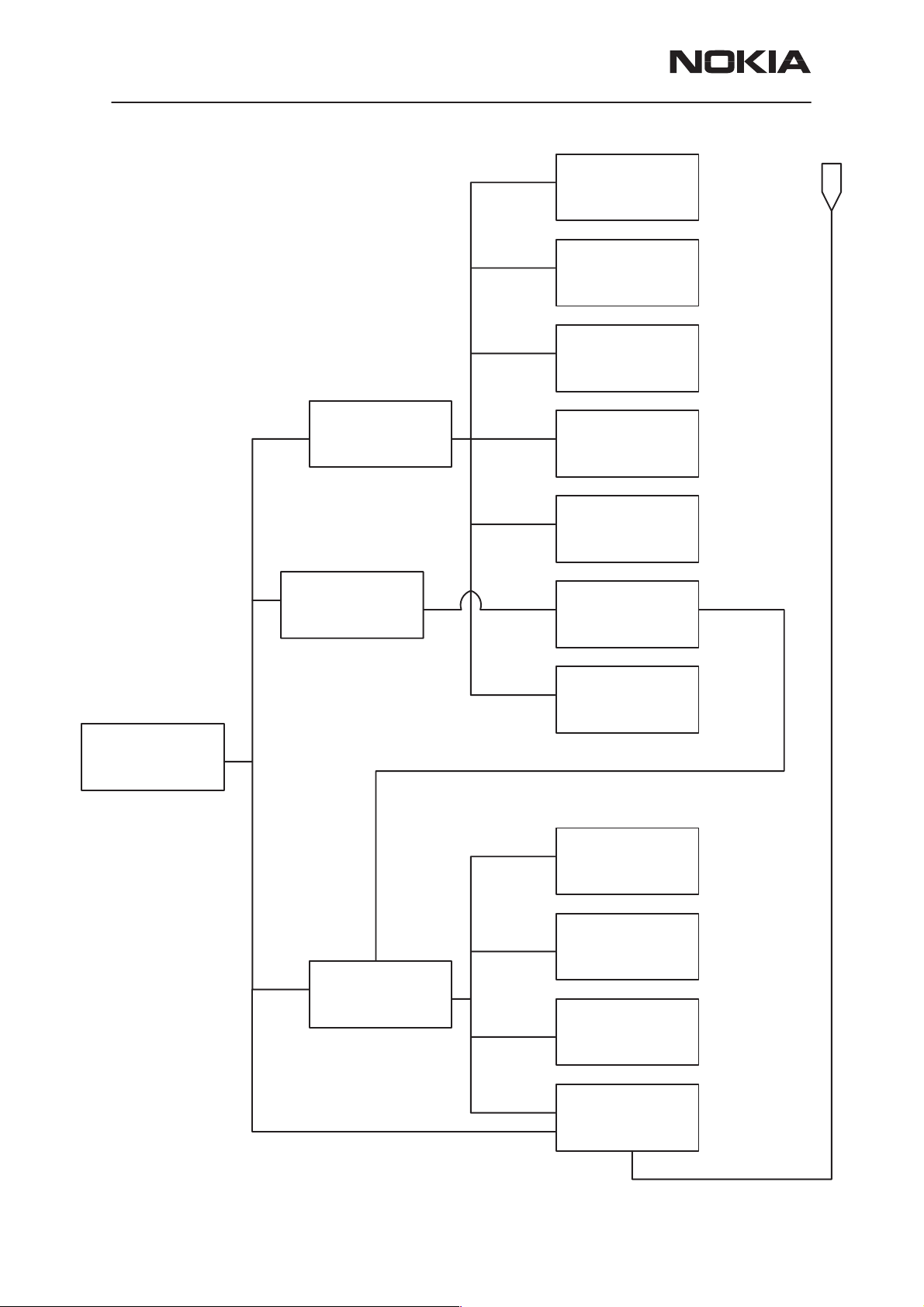
THF-12
System Module NH1
Current Consumption
VRX
12 mA
2 mA
2 mA
PAMS Technical Documentation
LNA
TXE
IF amplifier
IF circuit
Battery
Battery
3.6 V
regulator
2.7 V
VPLL
regulator
2.7 V
7
LO buffer
15 mA
RX–VCO
10 mA
Synthesizer IC
4 mA
VCTCXO
TXSYNE
15 mA
TX–VCO
Page 46
20 mA
regulator
2.7 V
20 mA
VTX
3 mA
950 mA
Nokia Mobile Phones Ltd.
TX buffer
TX power
control
PA
Issue 3 02/2000
Page 47

PAMS Technical Documentation
System Module NH1
Connections
Connections to Baseband sub–module
Table 13. Connections to BB module
Signal Name Type Function
AFC Analog in The reference oscillator frequency adjust.
FMCTRL Analog.out FM radio VCO control
FMLOS Analog.in FM radio VCO signal for PLL
IF Analog out 2nd IF signal
MOD Analog in Modulation signal for transmitter (Audio + data)
RFTEMP Analog out RF temperature, which is determined by NTC resistor.
THF-12
RSSI Analog out Received signal strength indicator. Voltage measurement.
SCLK Digital in Serial clock for synthesizer. Active state: Rising edge
SDATA Digital in Serial data for synthesizer. Active state: High
SLE Digital in Synthesizer enable. Active state: High
TXC PWM in Transmitter power control
TXE Digital in Transmitter on/off. High when on.
TXSYNE Analog out TX synthesizer power control
VBAT Power Battery voltage
VPLL Power Regulated voltage for synthesizer IC
VRX Power Regulated voltage for receiver & receiver synth
VPLL Power Regulated voltage for transmitter synth
Table 14. Values for digital control signal
Supply voltage VDD 2.7 V
Logical 1 VOH VDD*0,7...VDD+0.3V
Logical 0 VOL –0.3V...VDD*0,3
Logical 1 IOH <5mA
Logical 0 IOL <5mA
CLKIN 14.85 MHz VCTCXO signal
Level 1 Vpp min
Load impedance 10 k W\\10pF +/– 10%
Start time < 60 mS after Vref rising
Issue 3 02/2000
Table 15. VCTCXO signal specifications
Nokia Mobile Phones Ltd.
Page 47
Page 48

THF-12
System Module NH1
AFC VCTCXO control voltage
Type analog signal (DC–level)
Level 0.1...2.7 V DC
Load impedance ZL > 10 kW
Control step size < 12 mV
IF 450 kHz 2nd IF signal
Level 300 mVp–p (typical) not speci-
Source impedance < 1.0 kW
PAMS Technical Documentation
Table 16. VCTCXO control signal specifications
Table 17. IF signal
fied by manufacturer
Table 18. MOD signal
MOD Modulation signal for trans-
mitter (Audio + data)
Type Analog signal
Nominal level 300 mV rms @3.0 kHz deviation
Load impedance ZL > 22 kW
Table 19. RSSI signal
RSSI Received signal strength in-
dicator
DC–level 0,5...1.6 V (–115...–45 dBm)
dynamic range 70 dB
Source impedance 56 kW
Table 20. SCLK signal
SCLK Serial clock for synthesizer
Type digital signal
Page 48
Pulse width > 1 us
Table 21. SDAT signal
SDAT Serial data for synthesizer
Type digital signal
Pulse width > 1 us
VALUES
Control byte xx100 000x x10000xx
(synte_initial_const)
Nokia Mobile Phones Ltd.
Issue 3 02/2000
Page 49

PAMS Technical Documentation
Serial data for synthesizerSDAT
Reference divider 1188 (25 kHz channel)
THF-12
System Module NH1
Table 21. SDAT signal
Divider formulas for TX oscil-
lator
Divider formulas for RX oscil-
lator
Table 22. SLE signal
SLE Synthesizer enable
Type Digital signal
Function 0 = synthesizer enabled
Table 23. RXE signal
RXE Receiver enable
Type Digital signal
Function 0 = Receiver off
On–state current < 100 uA
(TX_synte_base_const1
(RX_synte_base_const1
1 = synthesizer disabled
N = 2*ch +36238
8D,8E)
N = 2*ch +33438
82,9E)
1 = Receiver on
Table 24. TXC signal
TXC Transmitter power control
Type PWM signal
Function Duty cycle of the TXC signal
defines the TX power level.
PWM frequency 30 kHz (7.2 kHz)
Level 0...3.3 V DC
Number of duty cycle steps 256
Load impedance > 100 kohm
Table 25. TXE signal
TXE Transmitter on/off control
Type Digital signal
Function 0 = TX off
Issue 3 02/2000
Nokia Mobile Phones Ltd.
1 = TX on
Page 49
Page 50

THF-12
System Module NH1
VBAT Battery voltage
Nominal value 3.6 V
Minimum value 3.2 V
Absolute maximum 5.2 V
Max. current 1.3 A
Antenna
The phone is fitted with a retractable antenna. The electrical length of antenna is 1/4 wave length.
Receiver
The receiver is a dual–conversion superheterodyne using two intermediate frequencies, 45 MHz and 450 kHz.
PAMS Technical Documentation
Table 26. VBAT voltage
The RF signal from the duplexer RX port is applied to the low noise RF
amplifier. The amplifier comprises the transistor V310. The amplifier
stage input matching comprises C301, C302 and L301. R301 and R311
are included for biasing. The output matching comprises L311, C312
and C313.
The AGC circuit comprises V320 and V321. The AGC–off current is adjusted by R323. The AGC–on current is determined by R323 and R324.
Next the signal is filtered with Z330. After the filter the signal is fed to a
single balanced diode mixer, comprising Z331, Z332, Z350 and V330.
After the mixer the 45 MHz IF signal is filtered with the crystal filter Z340.
Matching between the mixer and the filter comprises L340, R340, C340
and C341. Next the IF signal is amplified by V360. The input matching
comprises R341. The biasing comprises R360, R361 and R363. Capacitors C360 and C361 are included for RF bypassing.
The second mixer, IF amplifier and quadrature detector are all integrated
in the circuit N370. The second LO frequency, 44.55 MHz, is the third
harmonic of the VCTCXO frequency. The LO signal tank circuit comprises C372 and L371. After the mixer the 450kHz IF signal is filtered
with the ceramic filter Z370.
The RSSI and 2nd IF signal (450 kHz) are fed to the audio/logic unit.
RX Synthesizer
The first injection frequency is generated by a digital phase locked loop
(PLL). The PLL comprises a VCO, a loop filter and a PLL IC which includes reference and main dividers. The output frequency of the loop
(LO) is obtained from a voltage–controlled oscillator (VCO) G520. Output
level of VCO is 0 dBm +/– 2 dB. The VCO output signal is amplified by
Page 50
Nokia Mobile Phones Ltd.
Issue 3 02/2000
Page 51

PAMS Technical Documentation
transistor V350 and fed to the receiver mixer via Z350. A portion of output signal is fed back to the synthesizer.
The overall divisor of the chain is selected according to the desired channel.
The internal dividers of N400 are programmed with 17 bits, which are
transferred serially on the SDATA (synthesizer data) line from the processor into an internal shift register also located in N400. Data transfer is
timed with SCLK clock pulses.
The divided frequency is compared with a highly stable reference frequency from VCTCXO by a phase comparator in the PLL circuit (N400).
The phase comparator controls the VCO frequency by means of a DC
voltage through the loop filter so as to keep the divided frequency applied
to the phase comparator equal to the fixed reference frequency.
The reference frequency is 12.5 kHz. This reference frequency is obtained from voltage controlled temperature compensated crystal oscillator
(VCTCXO). The oscillator frequency is 14.85 MHz. The VCTCXO frequency is divided by 1188.
THF-12
System Module NH1
RX loop filter
The Phase comparator output is pin 3. If the VCO frequency is too high,
the output goes low and discharge integrator capacitor C421. After this,
the DC control voltage and the VCO frequency will decrease.
If the VCO frequency is too low, the output goes high and charge the integrator capacitor C421. Thereafter the DC control voltage and the VCO
frequency will go up.
Output pulses from the phase detector are fed to the loop filter. The function of the integrator is to convert positive and negative pulses to DC voltage. The remaining ripple and AC components are filtered in a three
stage lowpass filter.
TX Synthesizer
The transmitter synthesizer generates a frequency modulated transmitter
signal to the transmitter section. The injection frequency for transmitter is
generated by a digital phase locked loop (PLL). The modulated TX frequency is generated in TX–VCO (G430). The output level of the VCO is
0 dBm +/– 2 dB. After the VCO the TX signal is amplified in the TX buffer
V440 before power amplifier module. The gain in the TX buffer is about 8
dB.
If there is a problem with transmitter PA output power, adaptive gain control of TX buffer will increase the injection signal level to transmitter PA. If
the PA control voltage rises over 2.3 V, it is assumed that PA is not capable to obtain 750 mW output power anymore. In that case the network of
the double operation amplifier N401 will change the V440 biasing point to
maximize TX output power.
Issue 3 02/2000
Nokia Mobile Phones Ltd.
Page 51
Page 52

THF-12
System Module NH1
TX Loop Filter
Output pulses from the phase detector N400 pin 17 are supplied to the
loop filter. The integrator, which constitutes R433, C435 and C436, converts positive and negative pulses to DC voltage. The remaining ripple is
filtered in a three stage low–pass filter.
Transmitter
The transmitter constitutes a power amplifier module (N611). The modulated RF signal from the TX synthesizer is applied to the 50 ohm input of
the transmitter module. The power level is controlled by a voltage which
is supplied to pin 16 of the PA module. A voltage proportional to the output power is rectified from a coupler strip by the DC–biased Schottky
diode V634. This rectified voltage is fed to a differential amplifier which
comprises transistors V631 and V632 .
PAMS Technical Documentation
The reference voltage to control the PA module is filtered from the PWM
signal TXC to DC voltage by a two stage lowpass filter. The differential
amplifier adjusts the collector voltage of the transistor V630 so that the
reference voltage and the voltage proportional to the output power are
equal. The transmitter is switched on when TXE goes high (logic 1),
which enables the transmitter power control circuit by transistor V611.
When the transmitter is inactive (TXE low) the RF level from the transmitter is reduced below –57 dBm.
RF Characteristics
Ambient temperature
Line Symbol Minimum Typical /
Nominal
Operating temperature –25 +55 °C
Maximum Unit / Notes
Duplexer
Transmitter Receiver
Frequency 453...457.475 MHz 463...467.475 MHz
Insertion loss max 2.8 dB 6 dB
Ripple at BW max 1.5 dB 1.5 dB
Termination impedance 50 W 50 W
Permissible input power 2.5 W
Page 52
Nokia Mobile Phones Ltd.
Issue 3 02/2000
Page 53

PAMS Technical Documentation
RX submodule
Table 27. RX Specification
THF-12
System Module NH1
N=Normal
E=Extreme
conditions
N RF–sensitivity < –113 dBm (SINAD 20 dB)
E RF–sensitivity < –110 dBm (SINAD 20 dB)
N Adjacent channel selectivity > 67 dB (25 kHz)
E Adjacent channel selectivity > 60 dB (25 kHz)
N Spurious response rejection > 67 dB
N Intermodulation rejection > 67 dB
N RX–band excluding the receiver freq.
N Spurious emissions
N 100 kHz ... 1000 MHz < –57 dBm
N 1000 MHz ... 4000 MHz < –47 dBm
N / E Audio harmonic distortion < 5 %
Characteristic Unit / Notes
Frequency range 463...467.475 MHz
Type FM receiver, 2 IFs
Intermediate Frequencies 45 MHz, 450 kHz
Blocking :
> –87dB
10 MHz
N / E Noise & hum < –35 dB
N / E RSSI dynamic range > 65 dB
N / E AGC attenuation 5...10 dB
Issue 3 02/2000
Nokia Mobile Phones Ltd.
Page 53
Page 54

THF-12
System Module NH1
Preamplifier
PAMS Technical Documentation
Table 28. Preamplifier specifications
Minimum Typical /
Nominal
Supply voltage 2,7 V
Frequency band 463 467,475 MHz
Current consumption (AGC off) 9 7 mA
Current consumption (AGC on) 2 mA
Insertion gain (AGC off) 19 22 dB
Insertion gain (AGC on) 14 dB
Gain flatness ±1 dB
Noise figure 1.6 1.8 dB
Reverse isolation 30 40 dB
IIP3 –5 dBm
Input return loss (Z0=50W) –4 dB
Output return loss (Z0=50W) –11 dB
Maximum Unit / Notes
RX–filter
Table 29. RX–filter specification
Minimum Typical /
Nominal
Center frequency, f
Bandwidth (–0,8 dB) ±3 MHz
Stopband attenuation
f0 -10 MHz
f0 -90 MHz
Insertion loss 3,7 4 dB
Passband ripple 0,7 1,0 dB
Terminating impedance 50W // 18nH
0
12
45
464,5 MHz
15 dB
50 dB
Maximum Unit / Notes
1st mixer
Table 30. 1st mixer specification
Minimum Typical /
Nominal
Frequency band
RF 463 467.475 MHz
Maximum Unit / Notes
LO 418 422.475 MHz
Page 54
Nokia Mobile Phones Ltd.
Issue 3 02/2000
Page 55

PAMS Technical Documentation
Table 30. 1st mixer specification (continued)
THF-12
System Module NH1
Minimum
Nominal
IF 45 MHz
Conversion loss 6 8 dB
IIP3 12 dBm
IIP2 18 dBm
LO power level 0 dBm
LO–RF isolation 30 dB
Unit / NotesMaximumTypical /
1st IF–filter
Table 31. 1st if–filter specification
Minimum Typical / Nomi-
nal
Type Crystal 4–pole
Center frequency, f
Operating temperature –25 +85 °C
3dB bandwidth ± 7,5 kHz Passband
Stopband attenuation
0
45,000 MHz
Maximum Unit / Notes
fo ± 22 kHz 25 dB adj channel
fo -900 kHz ± 10 kHz 80 dB 2nd mirror
Spurious response rejec-
tion
fo±150 ... ±1000 kHz
Insertion loss 3 dB
Passband ripple 1 dB
Terminating impedance 600 // 2 W // pF
Group delay distortion 30 ms at f0 ± 5 kHz
40 dB
IF–amplifier
Table 32. IF–amplifier specification
Minimum Typical /
Nominal
Operating frequency 45 MHz
Supply voltage 2.7 V
Input impedance 800 // 1.5 W // pF
Output impedance 1000 W
Maximum Unit / Notes
Insertion gain 15 18 dB
Noise figure 3 dB
IIP3 –30 dBm
Issue 3 02/2000
Nokia Mobile Phones Ltd.
Page 55
Page 56

THF-12
System Module NH1
2nd IF–filter
PAMS Technical Documentation
Table 33. 2nd if–filter specification
Minimum Typical /
Nominal
Center frequency 450 kHz
Temperature range +10 (–30) +50 (+70) °C
6 dB bandwidth ± 6.0 (5,5) kHz
26 dB bandwidth ± 9.0 (10,0) kHz
50 dB bandwidth ± 12,5 (13,0) kHz
Insertion loss 5,0 (6,0) dB
Ripple 3,0 (4,0) dB
Stopband attenuation
f0 ±13 ... 25 kHz
f0 ±25 ... 100
kHz
Spurious response rejection 0,1...1MHz
Group delay time 100 (120) ms at f0 ±4 kHz
Input & output imped-
ance
40
35
20 dB
1,35 1,5 1,65 kW
Maximum Unit / Notes
dB
dB
IF–circuit
Table 34. IF circuit specification
Minimum Typical /
Nominal
Supply voltage 2.7 V
Current consumption 2,0 mA
2. lo frequency 44.550 MHz
RSSI dynamic range 70 dB
Case 16 SSOP
Maximum Unit / Notes
TX submodule
Table 35. TX Specification
N=Normal
E=Extreme
conditions
Frequency range 453...457.475 MHz
N / E Frequency error ± 2.5 kHz
Unit / Notes
N / E Output power (after duplex filter) at all
channels
Page 56
Nokia Mobile Phones Ltd.
Issue 3 02/2000
Page 57

PAMS Technical Documentation
Table 35. TX Specification (continued)
E=Extreme
conditions
N / E PL 0,1 21.76 ( ± 2 / 3) dBm
N / E PL 2,3 31.76 ( ± 2 / 3) dBm
System Module NH1
Unit / Notes N=Normal
THF-12
N / E Carrier switching time from – 40 dB to its
steady state power and frequency within
±1 kHz final frequency
Spurious emissions
N 100 kHz ... 1000 MHz (tx operating) < –36 dBm
N 100 kHz ... 1000 MHz (standby) < –57 dBm
N 1000 MHz ... 4000 MHz (tx operating) < –30 dBm
N 1000 MHz ... 4000 MHz (standby) < –47 dBm
N Frequency deviation <± 4.7 KHz
N / E Limiting characteristics of modulator ± 3.7 ...4.7 KHz
N Adjacent channel power >67dB
N / E Harmonic distortion <5%
N Residual modulation (CCITT on) < -40 dB
N Residual modulation (CCITT off) < -20 dB
< 6 ms
Power amplifier
Table 36. Power amplifier specification
Minimum Typical /
Nominal
Supply voltage 3.2 3.6 4.5 V (5.3V in idle mode)
Current consumption 750 1000 mA (at P
Input power 2 10 dBm
Output power 31.8 dBm (1.5W)
Efficiency 50 % (at operation point)
Harmonic level –15 dB (at 2*f
Harmonic level –20 dB (at 3*f
Input VSWR 2:1 4:1
Output VSWR
Issue 3 02/2000
Nokia Mobile Phones Ltd.
Maximum Unit / Notes
= 1.5W)
out
)
carrier
and hig-
her)
20:1 No degradation or de-
stroy
6:1 No parasitic oscillation
carrier
Page 57
Page 58

THF-12
System Module NH1
Power control
PAMS Technical Documentation
Table 37. Power control specification
Minimum Typical /
Nominal
Supply voltage V
Drive current 5.0 mA
Power control range 32 dB
Control step size 10 15 mW
Maximum Unit / Notes
Coupler lines
Table 38. Directional coupler specification
Minimum Typical /
Nominal
Coupling coefficient 18 25 22 dB
VSWR input (Z0=50W) 1:1.2
Isolation 15 dB (with 50 ohm in/out)
Insertion loss 0.25 dB (with 50 ohm in/out)
Maximum Unit / Notes
Synthesizer submodule
PLL
Table 39. PLL specification
Minimum Typical /
Nominal
Frequency band 400 1100 MHz
Channel separation 25 kHz
Supply voltage 2.6 2.75 5.5 V
Current consumption 10.0 mA
RX VCO
Table 40. RX VCO specification
Minimum Typical /
Nominal
Frequency band 415.000 425.000 MHz
Operating temperature –30 +80
Maximum Unit / Notes
Maximum Unit / Notes
o
C
Output level –3 +0 +3 dBm / 50 W
Page 58
Nokia Mobile Phones Ltd.
Issue 3 02/2000
Page 59

PAMS Technical Documentation
Table 40. RX VCO specification (continued)
THF-12
System Module NH1
Minimum
Nominal
Harmonic attenuation 12 dB
Frequency pulling
due to load
variations
due to supply
voltage
Supply voltage 2.5 2.7 3.0 V
Current consumption 12 mA
SSB phase noise –118 dBc/Hz (20 kHz offset,
Control Voltage 1.75 4.75
SNR without vibration –44 dB (± 3 kHz dev at
SNR with vibration –34 dB (± 3 kHz dev at
±200 kHz (VSWR = 2.0)
±200 kHz (Vcc ± 0.5 V)
Unit / NotesMaximumTypical /
1Hz BW)
1kHz)
1kHz, at 55 to 150 Hz,
for 15 m/s2 acceleration)
TX VCO
Table 41. TX VCO specification
Minimum Typical /
Nominal
Frequency band 450.000 460.000 MHz
Operating temperature –30 +80
Output level –1 +1 +3 dBm / 50 W
Harmonic attenuation 12 dB
Frequency pulling
due to load
variations
due to supply
voltage
Modulation
mod. sensitivity 300 mV
Supply voltage 2.6 2.7 3.0 V
Maximum Unit / Notes
o
C
±200 kHz (VSWR = 2.0)
±200 kHz (Vcc ± 0.5 V)
/ 3 kHz devi-
rms
ation
Current consumption 12 mA
Issue 3 02/2000
Nokia Mobile Phones Ltd.
Page 59
Page 60

THF-12
System Module NH1
PAMS Technical Documentation
Table 41. TX VCO specification (continued)
Minimum
Nominal
SSB phase noise –117 dBc/Hz (20 kHz offset,
SNR without vibration –44 dB (± 3 kHz dev at
SNR with vibration –34 dB (± 3 kHz dev at
Unit / NotesMaximumTypical /
1Hz BW)
1kHz)
1kHz, at 55 to 150 Hz,
for 15 m/s2 acceleration)
Isolation amplifier (TX buffer)
Table 42. TX buffer specification
Minimum Typical /
Nominal
Frequency range 410 490 MHz
Input power –1.5 0 +1.5 dBm
Output power 4 10 dBm
Reverse isolation 30 dB
Maximum Unit / Notes
Supply voltage 2.75 V
Current consumption 8 40 mA
VCTCXO
Table 43. VCTCXO specification
Minimum Typical /
Nominal
Frequency 14,85 MHz
Control voltage 0.3 3,0 V
frequency accuracy ± 2.5 ppm
Output level 1 Vpp AC
Supply voltage 2.7 V
Current consumption 2 mA
Maximum Unit / Notes
Page 60
Nokia Mobile Phones Ltd.
Issue 3 02/2000
Page 61

THF-12
PAMS Technical Documentation
System Module NH1
Parts list of NH1 Basic (EDMS Issue 4.5) Code: 0201267
ITEM CODE DESCRIPTION VALUE TYPE
R102 1422881 Chip resistor 0.22 5 % 1 W 1218
R103 1430145 Chip resistor 100 k 1 % 0.063 W 0402
R104 1430842 Chip resistor 680 k 1 % 0.063 W 0402
R105 1430778 Chip resistor 10 k 5 % 0.063 W 0402
R106 1430842 Chip resistor 680 k 1 % 0.063 W 0402
R107 1430145 Chip resistor 100 k 1 % 0.063 W 0402
R111 1430796 Chip resistor 47 k 5 % 0.063 W 0402
R113 1430764 Chip resistor 3.3 k 5 % 0.063 W 0402
R121 1430792 Chip resistor 33 k 5 % 0.063 W 0402
R122 1430792 Chip resistor 33 k 5 % 0.063 W 0402
R123 1430778 Chip resistor 10 k 5 % 0.063 W 0402
R130 1430804 Chip resistor 100 k 5 % 0.063 W 0402
R131 1430804 Chip resistor 100 k 5 % 0.063 W 0402
R132 1430792 Chip resistor 33 k 5 % 0.063 W 0402
R133 1430690 Chip jumper 0402
R140 1430778 Chip resistor 10 k 5 % 0.063 W 0402
R141 1430788 Chip resistor 22 k 5 % 0.063 W 0402
R142 1430804 Chip resistor 100 k 5 % 0.063 W 0402
R148 1430766 Chip resistor 3.9 k 5 % 0.063 W 0402
R149 1430780 Chip resistor 12 k 5 % 0.063 W 0402
R150 1430784 Chip resistor 15 k 5 % 0.063 W 0402
R151 1430776 Chip resistor 8.2 k 5 % 0.063 W 0402
R152 1430776 Chip resistor 8.2 k 5 % 0.063 W 0402
R153 1430784 Chip resistor 15 k 5 % 0.063 W 0402
R154 1430784 Chip resistor 15 k 5 % 0.063 W 0402
R155 1430784 Chip resistor 15 k 5 % 0.063 W 0402
R156 1430784 Chip resistor 15 k 5 % 0.063 W 0402
R157 1430784 Chip resistor 15 k 5 % 0.063 W 0402
R158 1430784 Chip resistor 15 k 5 % 0.063 W 0402
R159 1430784 Chip resistor 15 k 5 % 0.063 W 0402
R160 1430778 Chip resistor 10 k 5 % 0.063 W 0402
R161 1430778 Chip resistor 10 k 5 % 0.063 W 0402
R162 1430778 Chip resistor 10 k 5 % 0.063 W 0402
R163 1430778 Chip resistor 10 k 5 % 0.063 W 0402
R164 1430778 Chip resistor 10 k 5 % 0.063 W 0402
R165 1430776 Chip resistor 8.2 k 5 % 0.063 W 0402
R166 1430776 Chip resistor 8.2 k 5 % 0.063 W 0402
R167 1430776 Chip resistor 8.2 k 5 % 0.063 W 0402
R168 1430776 Chip resistor 8.2 k 5 % 0.063 W 0402
R169 1430776 Chip resistor 8.2 k 5 % 0.063 W 0402
R170 1430776 Chip resistor 8.2 k 5 % 0.063 W 0402
R171 1430762 Chip resistor 2.2 k 5 % 0.063 W 0402
R172 1430700 Chip resistor 10 5 % 0.063 W 0402
R173 1430812 Chip resistor 220 k 5 % 0.063 W 0402
Issue 3 02/2000
Nokia Mobile Phones Ltd.
Page 61
Page 62

THF-12
System Module NH1
R174 1430812 Chip resistor 220 k 5 % 0.063 W 0402
R175 1430796 Chip resistor 47 k 5 % 0.063 W 0402
R176 1430796 Chip resistor 47 k 5 % 0.063 W 0402
R179 1430778 Chip resistor 10 k 5 % 0.063 W 0402
R180 1430778 Chip resistor 10 k 5 % 0.063 W 0402
R182 1825005 Chip varistor vwm14v vc30v 0805 0805
R183 1430796 Chip resistor 47 k 5 % 0.063 W 0402
R184 1430706 Chip resistor 15 5 % 0.063 W 0402
R185 1430706 Chip resistor 15 5 % 0.063 W 0402
R186 1430690 Chip jumper 0402
R187 1430804 Chip resistor 100 k 5 % 0.063 W 0402
R189 1825005 Chip varistor vwm14v vc30v 0805 0805
R195 1430754 Chip resistor 1.0 k 5 % 0.063 W 0402
R196 1430804 Chip resistor 100 k 5 % 0.063 W 0402
R197 1430804 Chip resistor 100 k 5 % 0.063 W 0402
R198 1430734 Chip resistor 220 5 % 0.063 W 0402
R202 1430145 Chip resistor 100 k 1 % 0.063 W 0402
R203 1430778 Chip resistor 10 k 5 % 0.063 W 0402
R204 1430792 Chip resistor 33 k 5 % 0.063 W 0402
R205 1430792 Chip resistor 33 k 5 % 0.063 W 0402
R206 1430778 Chip resistor 10 k 5 % 0.063 W 0402
R207 1430754 Chip resistor 1.0 k 5 % 0.063 W 0402
R208 1430770 Chip resistor 4.7 k 5 % 0.063 W 0402
R210 1430770 Chip resistor 4.7 k 5 % 0.063 W 0402
R215 1430187 Chip resistor 47 k 1 % 0.063 W 0402
R216 1430778 Chip resistor 10 k 5 % 0.063 W 0402
R217 1430792 Chip resistor 33 k 5 % 0.063 W 0402
R230 1430796 Chip resistor 47 k 5 % 0.063 W 0402
R231 1430778 Chip resistor 10 k 5 % 0.063 W 0402
R241 1430792 Chip resistor 33 k 5 % 0.063 W 0402
R242 1430792 Chip resistor 33 k 5 % 0.063 W 0402
R243 1430792 Chip resistor 33 k 5 % 0.063 W 0402
R301 1430774 Chip resistor 6.8 k 5 % 0.063 W 0402
R310 1430714 Chip resistor 33 5 % 0.063 W 0402
R311 1430724 Chip resistor 82 5 % 0.063 W 0402
R312 1430720 Chip resistor 56 5 % 0.063 W 0402
R313 1430740 Chip resistor 330 5 % 0.063 W 0402
R314 1430690 Chip jumper 0402
R320 1430754 Chip resistor 1.0 k 5 % 0.063 W 0402
R323 1430746 Chip resistor 560 5 % 0.063 W 0402
R324 1430808 Chip resistor 150 k 5 % 0.063 W 0402
R325 1430760 Chip resistor 1.8 k 5 % 0.063 W 0402
R340 1430690 Chip jumper 0402
R341 1430734 Chip resistor 220 5 % 0.063 W 0402
R351 1430728 Chip resistor 120 5 % 0.063 W 0402
R352 1430770 Chip resistor 4.7 k 5 % 0.063 W 0402
R353 1430772 Chip resistor 5.6 k 5 % 0.063 W 0402
R354 1430760 Chip resistor 1.8 k 5 % 0.063 W 0402
PAMS Technical Documentation
Page 62
Nokia Mobile Phones Ltd.
Issue 3 02/2000
Page 63

THF-12
PAMS Technical Documentation
R355 1430740 Chip resistor 330 5 % 0.063 W 0402
R360 1430784 Chip resistor 15 k 5 % 0.063 W 0402
R361 1430788 Chip resistor 22 k 5 % 0.063 W 0402
R362 1430710 Chip resistor 22 5 % 0.063 W 0402
R363 1430746 Chip resistor 560 5 % 0.063 W 0402
R373 1430714 Chip resistor 33 5 % 0.063 W 0402
R374 1430804 Chip resistor 100 k 5 % 0.063 W 0402
R381 1430754 Chip resistor 1.0 k 5 % 0.063 W 0402
R401 1430710 Chip resistor 22 5 % 0.063 W 0402
R402 1430710 Chip resistor 22 5 % 0.063 W 0402
R403 1430796 Chip resistor 47 k 5 % 0.063 W 0402
R404 1430796 Chip resistor 47 k 5 % 0.063 W 0402
R405 1430796 Chip resistor 47 k 5 % 0.063 W 0402
R407 1430796 Chip resistor 47 k 5 % 0.063 W 0402
R408 1430748 Chip resistor 680 5 % 0.063 W 0402
R409 1430690 Chip jumper 0402
R410 1430754 Chip resistor 1.0 k 5 % 0.063 W 0402
R412 1430796 Chip resistor 47 k 5 % 0.063 W 0402
R413 1430748 Chip resistor 680 5 % 0.063 W 0402
R414 1430754 Chip resistor 1.0 k 5 % 0.063 W 0402
R415 1430754 Chip resistor 1.0 k 5 % 0.063 W 0402
R416 1430778 Chip resistor 10 k 5 % 0.063 W 0402
R424 1430734 Chip resistor 220 5 % 0.063 W 0402
R425 1430734 Chip resistor 220 5 % 0.063 W 0402
R430 1430700 Chip resistor 10 5 % 0.063 W 0402
R431 1430690 Chip jumper 0402
R432 1430784 Chip resistor 15 k 5 % 0.063 W 0402
R437 1430820 Chip resistor 470 k 5 % 0.063 W 0402
R438 1430820 Chip resistor 470 k 5 % 0.063 W 0402
R440 1430734 Chip resistor 220 5 % 0.063 W 0402
R441 1430734 Chip resistor 220 5 % 0.063 W 0402
R445 1430740 Chip resistor 330 5 % 0.063 W 0402
R446 1430700 Chip resistor 10 5 % 0.063 W 0402
R447 1430754 Chip resistor 1.0 k 5 % 0.063 W 0402
R480 1430778 Chip resistor 10 k 5 % 0.063 W 0402
R482 1430778 Chip resistor 10 k 5 % 0.063 W 0402
R483 1430778 Chip resistor 10 k 5 % 0.063 W 0402
R484 1430800 Chip resistor 68 k 5 % 0.063 W 0402
R485 1430780 Chip resistor 12 k 5 % 0.063 W 0402
R486 1430762 Chip resistor 2.2 k 5 % 0.063 W 0402
R487 1430778 Chip resistor 10 k 5 % 0.063 W 0402
R488 1430804 Chip resistor 100 k 5 % 0.063 W 0402
R489 1430774 Chip resistor 6.8 k 5 % 0.063 W 0402
R490 1430754 Chip resistor 1.0 k 5 % 0.063 W 0402
R491 1430774 Chip resistor 6.8 k 5 % 0.063 W 0402
R613 1430778 Chip resistor 10 k 5 % 0.063 W 0402
R615 1430778 Chip resistor 10 k 5 % 0.063 W 0402
R622 1430712 Chip resistor 27 5 % 0.063 W 0402
System Module NH1
Issue 3 02/2000
Nokia Mobile Phones Ltd.
Page 63
Page 64

THF-12
System Module NH1
R631 1430788 Chip resistor 22 k 5 % 0.063 W 0402
R632 1430788 Chip resistor 22 k 5 % 0.063 W 0402
R633 1430778 Chip resistor 10 k 5 % 0.063 W 0402
R634 1430754 Chip resistor 1.0 k 5 % 0.063 W 0402
R635 1430790 Chip resistor 27 k 5 % 0.063 W 0402
R637 1430778 Chip resistor 10 k 5 % 0.063 W 0402
R638 1430784 Chip resistor 15 k 5 % 0.063 W 0402
R639 1430784 Chip resistor 15 k 5 % 0.063 W 0402
R640 1430718 Chip resistor 47 5 % 0.063 W 0402
R641 1430718 Chip resistor 47 5 % 0.063 W 0402
R642 1430754 Chip resistor 1.0 k 5 % 0.063 W 0402
R701 1430762 Chip resistor 2.2 k 5 % 0.063 W 0402
R712 1430830 Chip resistor 1.0 M 5 % 0.063 W 0402
R713 1430770 Chip resistor 4.7 k 5 % 0.063 W 0402
R714 1430812 Chip resistor 220 k 5 % 0.063 W 0402
R731 1430762 Chip resistor 2.2 k 5 % 0.063 W 0402
R732 1430804 Chip resistor 100 k 5 % 0.063 W 0402
R734 1430762 Chip resistor 2.2 k 5 % 0.063 W 0402
R735 1430762 Chip resistor 2.2 k 5 % 0.063 W 0402
R744 1430690 Chip jumper 0402
R745 1430706 Chip resistor 15 5 % 0.063 W 0402
R746 1430706 Chip resistor 15 5 % 0.063 W 0402
R750 1430784 Chip resistor 15 k 5 % 0.063 W 0402
R751 1430788 Chip resistor 22 k 5 % 0.063 W 0402
R752 1430740 Chip resistor 330 5 % 0.063 W 0402
R753 1430744 Chip resistor 470 5 % 0.063 W 0402
R754 1430726 Chip resistor 100 5 % 0.063 W 0402
R761 1430788 Chip resistor 22 k 5 % 0.063 W 0402
R780 1430788 Chip resistor 22 k 5 % 0.063 W 0402
R781 1430754 Chip resistor 1.0 k 5 % 0.063 W 0402
R782 1430718 Chip resistor 47 5 % 0.063 W 0402
R784 1430804 Chip resistor 100 k 5 % 0.063 W 0402
R785 1430726 Chip resistor 100 5 % 0.063 W 0402
R786 1430744 Chip resistor 470 5 % 0.063 W 0402
R787 1430784 Chip resistor 15 k 5 % 0.063 W 0402
R788 1430788 Chip resistor 22 k 5 % 0.063 W 0402
R798 1430788 Chip resistor 22 k 5 % 0.063 W 0402
R800 1800673 NTC resistor 15 k 10 % 0.12 W 0805
C100 2320131 Ceramic cap. 33 n 10 % 16 V 0603
C101 2320779 Ceramic cap. 100 n 10 % 16 V 0603
C102 2604209 Tantalum cap. 1.0 u 20 % 16 V
3.2x1.6x1.6
C103 2320620 Ceramic cap. 10 n 5 % 16 V 0402
C105 2320620 Ceramic cap. 10 n 5 % 16 V 0402
C110 2611668 Tantalum cap. 4.7 u 20 % 10 V
3.2x1.6x1.6
C111 2320620 Ceramic cap. 10 n 5 % 16 V 0402
C112 2320620 Ceramic cap. 10 n 5 % 16 V 0402
PAMS Technical Documentation
Page 64
Nokia Mobile Phones Ltd.
Issue 3 02/2000
Page 65

THF-12
PAMS Technical Documentation
C113 2320620 Ceramic cap. 10 n 5 % 16 V 0402
C114 2320546 Ceramic cap. 27 p 5 % 50 V 0402
C115 2320546 Ceramic cap. 27 p 5 % 50 V 0402
C116 2610100 Tantalum cap. 1 u 20 % 10 V
2.0x1.3x1.2
C117 2320546 Ceramic cap. 27 p 5 % 50 V 0402
C118 2320546 Ceramic cap. 27 p 5 % 50 V 0402
C120 2610100 Tantalum cap. 1 u 20 % 10 V
2.0x1.3x1.2
C121 2610100 Tantalum cap. 1 u 20 % 10 V
2.0x1.3x1.2
C122 2320620 Ceramic cap. 10 n 5 % 16 V 0402
C123 2610100 Tantalum cap. 1 u 20 % 10 V
2.0x1.3x1.2
C140 2320131 Ceramic cap. 33 n 10 % 16 V 0603
C141 2320131 Ceramic cap. 33 n 10 % 16 V 0603
C160 2320544 Ceramic cap. 22 p 5 % 50 V 0402
C167 2320544 Ceramic cap. 22 p 5 % 50 V 0402
C168 2320584 Ceramic cap. 1.0 n 5 % 50 V 0402
C169 2320584 Ceramic cap. 1.0 n 5 % 50 V 0402
C170 2320131 Ceramic cap. 33 n 10 % 16 V 0603
C171 2320131 Ceramic cap. 33 n 10 % 16 V 0603
C172 2604127 Tantalum cap. 1.0 u 20 % 35 V
3.5x2.8x1.9
C180 2320516 Ceramic cap. 1.5 p 0.25 % 50 V 0402
C190 2320584 Ceramic cap. 1.0 n 5 % 50 V 0402
C191 2320584 Ceramic cap. 1.0 n 5 % 50 V 0402
C192 2320584 Ceramic cap. 1.0 n 5 % 50 V 0402
C193 2320584 Ceramic cap. 1.0 n 5 % 50 V 0402
C194 2320584 Ceramic cap. 1.0 n 5 % 50 V 0402
C195 2320584 Ceramic cap. 1.0 n 5 % 50 V 0402
C196 2320584 Ceramic cap. 1.0 n 5 % 50 V 0402
C197 2320584 Ceramic cap. 1.0 n 5 % 50 V 0402
C198 2320552 Ceramic cap. 47 p 5 % 50 V 0402
C201 2320779 Ceramic cap. 100 n 10 % 16 V 0603
C202 2320779 Ceramic cap. 100 n 10 % 16 V 0603
C203 2320779 Ceramic cap. 100 n 10 % 16 V 0603
C205 2320779 Ceramic cap. 100 n 10 % 16 V 0603
C206 2320779 Ceramic cap. 100 n 10 % 16 V 0603
C207 2320779 Ceramic cap. 100 n 10 % 16 V 0603
C208 2320546 Ceramic cap. 27 p 5 % 50 V 0402
C209 2320620 Ceramic cap. 10 n 5 % 16 V 0402
C228 2320620 Ceramic cap. 10 n 5 % 16 V 0402
C230 2320779 Ceramic cap. 100 n 10 % 16 V 0603
C231 2320620 Ceramic cap. 10 n 5 % 16 V 0402
C232 2610100 Tantalum cap. 1 u 20 % 10 V
2.0x1.3x1.2
C233 2312401 Ceramic cap. 1.0 u 10 % 10 V 0805
System Module NH1
Issue 3 02/2000
Nokia Mobile Phones Ltd.
Page 65
Page 66

THF-12
System Module NH1
C241 2320779 Ceramic cap. 100 n 10 % 16 V 0603
C242 2320779 Ceramic cap. 100 n 10 % 16 V 0603
C243 2320779 Ceramic cap. 100 n 10 % 16 V 0603
C251 2320779 Ceramic cap. 100 n 10 % 16 V 0603
C303 2320584 Ceramic cap. 1.0 n 5 % 50 V 0402
C310 2320560 Ceramic cap. 100 p 5 % 50 V 0402
C311 2312293 Ceramic cap. Y5 V 1206
C321 2320584 Ceramic cap. 1.0 n 5 % 50 V 0402
C330 2320548 Ceramic cap. 33 p 5 % 50 V 0402
C333 2320532 Ceramic cap. 6.8 p 0.25 % 50 V 0402
C340 2320604 Ceramic cap. 18 p 5 % 50 V 0402
C341 2320532 Ceramic cap. 6.8 p 0.25 % 50 V 0402
C342 2320532 Ceramic cap. 6.8 p 0.25 % 50 V 0402
C352 2320560 Ceramic cap. 100 p 5 % 50 V 0402
C353 2320532 Ceramic cap. 6.8 p 0.25 % 50 V 0402
C354 2320584 Ceramic cap. 1.0 n 5 % 50 V 0402
C360 2320584 Ceramic cap. 1.0 n 5 % 50 V 0402
C361 2320620 Ceramic cap. 10 n 5 % 16 V 0402
C362 2320620 Ceramic cap. 10 n 5 % 16 V 0402
C363 2320546 Ceramic cap. 27 p 5 % 50 V 0402
C370 2320584 Ceramic cap. 1.0 n 5 % 50 V 0402
C371 2320584 Ceramic cap. 1.0 n 5 % 50 V 0402
C372 2320546 Ceramic cap. 27 p 5 % 50 V 0402
C373 2320620 Ceramic cap. 10 n 5 % 16 V 0402
C374 2320620 Ceramic cap. 10 n 5 % 16 V 0402
C375 2312296 Ceramic cap. Y5 V 1210
C376 2320620 Ceramic cap. 10 n 5 % 16 V 0402
C381 2320620 Ceramic cap. 10 n 5 % 16 V 0402
C382 2320560 Ceramic cap. 100 p 5 % 50 V 0402
C401 2312293 Ceramic cap. Y5 V 1206
C402 2320620 Ceramic cap. 10 n 5 % 16 V 0402
C403 2320620 Ceramic cap. 10 n 5 % 16 V 0402
C404 2312293 Ceramic cap. Y5 V 1206
C405 2320620 Ceramic cap. 10 n 5 % 16 V 0402
C406 2610003 Tantalum cap. 10 u 20 % 10 V
3.2x1.6x1.6
C407 2312296 Ceramic cap. Y5 V 1210
C410 2312401 Ceramic cap. 1.0 u 10 % 10 V 0805
C411 2320620 Ceramic cap. 10 n 5 % 16 V 0402
C413 2320536 Ceramic cap. 10 p 5 % 50 V 0402
C414 2320620 Ceramic cap. 10 n 5 % 16 V 0402
C425 2320560 Ceramic cap. 100 p 5 % 50 V 0402
C426 2320131 Ceramic cap. 33 n 10 % 16 V 0603
C427 2320560 Ceramic cap. 100 p 5 % 50 V 0402
C430 2312293 Ceramic cap. Y5 V 1206
C431 2320560 Ceramic cap. 100 p 5 % 50 V 0402
C433 2320584 Ceramic cap. 1.0 n 5 % 50 V 0402
C434 2320560 Ceramic cap. 100 p 5 % 50 V 0402
PAMS Technical Documentation
Page 66
Nokia Mobile Phones Ltd.
Issue 3 02/2000
Page 67

THF-12
PAMS Technical Documentation
C440 2320602 Ceramic cap. 4.7 p 0.25 % 50 V 0402
C442 2320584 Ceramic cap. 1.0 n 5 % 50 V 0402
C443 2320584 Ceramic cap. 1.0 n 5 % 50 V 0402
C444 2320602 Ceramic cap. 4.7 p 0.25 % 50 V 0402
C447 2320540 Ceramic cap. 15 p 5 % 50 V 0402
C450 2320584 Ceramic cap. 1.0 n 5 % 50 V 0402
C451 2320524 Ceramic cap. 3.3 p 0.25 % 50 V 0402
C482 2320620 Ceramic cap. 10 n 5 % 16 V 0402
C483 2312401 Ceramic cap. 1.0 u 10 % 10 V 0805
C623 2320584 Ceramic cap. 1.0 n 5 % 50 V 0402
C628 2312401 Ceramic cap. 1.0 u 10 % 10 V 0805
C631 2320781 Ceramic cap. 47 n 20 % 16 V 0603
C632 2320781 Ceramic cap. 47 n 20 % 16 V 0603
C634 2320560 Ceramic cap. 100 p 5 % 50 V 0402
C637 2320560 Ceramic cap. 100 p 5 % 50 V 0402
C638 2320560 Ceramic cap. 100 p 5 % 50 V 0402
C639 2320618 Ceramic cap. 4.7 n 5 % 25 V 0402
C646 2320560 Ceramic cap. 100 p 5 % 50 V 0402
C651 2320560 Ceramic cap. 100 p 5 % 50 V 0402
C652 2320584 Ceramic cap. 1.0 n 5 % 50 V 0402
C653 2320620 Ceramic cap. 10 n 5 % 16 V 0402
C654 2320560 Ceramic cap. 100 p 5 % 50 V 0402
C655 2312401 Ceramic cap. 1.0 u 10 % 10 V 0805
C656 2320584 Ceramic cap. 1.0 n 5 % 50 V 0402
C657 2320560 Ceramic cap. 100 p 5 % 50 V 0402
C658 2312293 Ceramic cap. Y5 V 1206
C659 2320584 Ceramic cap. 1.0 n 5 % 50 V 0402
C660 2320560 Ceramic cap. 100 p 5 % 50 V 0402
C700 2320618 Ceramic cap. 4.7 n 5 % 25 V 0402
C701 2320544 Ceramic cap. 22 p 5 % 50 V 0402
C702 2320544 Ceramic cap. 22 p 5 % 50 V 0402
C703 2320779 Ceramic cap. 100 n 10 % 16 V 0603
C704 2320779 Ceramic cap. 100 n 10 % 16 V 0603
C705 2320779 Ceramic cap. 100 n 10 % 16 V 0603
C706 2320779 Ceramic cap. 100 n 10 % 16 V 0603
C712 2320620 Ceramic cap. 10 n 5 % 16 V 0402
C713 2320131 Ceramic cap. 33 n 10 % 16 V 0603
C714 2320620 Ceramic cap. 10 n 5 % 16 V 0402
C715 2312296 Ceramic cap. Y5 V 1210
C716 2320781 Ceramic cap. 47 n 20 % 16 V 0603
C717 2320131 Ceramic cap. 33 n 10 % 16 V 0603
C720 2320584 Ceramic cap. 1.0 n 5 % 50 V 0402
C732 2320620 Ceramic cap. 10 n 5 % 16 V 0402
C733 2320131 Ceramic cap. 33 n 10 % 16 V 0603
C734 2320131 Ceramic cap. 33 n 10 % 16 V 0603
C741 2320546 Ceramic cap. 27 p 5 % 50 V 0402
C749 2320576 Ceramic cap. 470 p 5 % 50 V 0402
C752 2320131 Ceramic cap. 33 n 10 % 16 V 0603
System Module NH1
Issue 3 02/2000
Nokia Mobile Phones Ltd.
Page 67
Page 68

THF-12
System Module NH1
C755 2320536 Ceramic cap. 10 p 5 % 50 V 0402
C756 2320620 Ceramic cap. 10 n 5 % 16 V 0402
C757 2320584 Ceramic cap. 1.0 n 5 % 50 V 0402
C758 2320584 Ceramic cap. 1.0 n 5 % 50 V 0402
C759 2320584 Ceramic cap. 1.0 n 5 % 50 V 0402
C760 2320584 Ceramic cap. 1.0 n 5 % 50 V 0402
C765 2320568 Ceramic cap. 220 p 5 % 50 V 0402
C767 2320560 Ceramic cap. 100 p 5 % 50 V 0402
C768 2320560 Ceramic cap. 100 p 5 % 50 V 0402
C781 2312296 Ceramic cap. Y5 V 1210
C783 2320131 Ceramic cap. 33 n 10 % 16 V 0603
C784 2320779 Ceramic cap. 100 n 10 % 16 V 0603
C786 2320556 Ceramic cap. 68 p 5 % 50 V 0402
C787 2320596 Ceramic cap. 3.3 n 5 % 50 V 0402
C788 2320596 Ceramic cap. 3.3 n 5 % 50 V 0402
C789 2320572 Ceramic cap. 330 p 5 % 50 V 0402
C790 2320620 Ceramic cap. 10 n 5 % 16 V 0402
C791 2610003 Tantalum cap. 10 u 20 % 10 V
3.2x1.6x1.6
C792 2320556 Ceramic cap. 68 p 5 % 50 V 0402
C793 2320560 Ceramic cap. 100 p 5 % 50 V 0402
C794 2320568 Ceramic cap. 220 p 5 % 50 V 0402
C795 2320779 Ceramic cap. 100 n 10 % 16 V 0603
C799 2320584 Ceramic cap. 1.0 n 5 % 50 V 0402
L102 3203701 Ferrite bead 33r/100mhz 0805 0805
L150 3203701 Ferrite bead 33r/100mhz 0805 0805
L151 3203701 Ferrite bead 33r/100mhz 0805 0805
L152 3641544 Chip coil 68 n 10 % Q=40/200 MHz
0805
L153 3645027 Chip coil 470 n 10 % Q=25/25 MHz
0805
L154 3645027 Chip coil 470 n 10 % Q=25/25 MHz
0805
L310 3643003 Chip coil 12 n 5 % Q=30/250 MHz
0805
L331 3641572 Chip coil 22 n 5 % Q=45/250 MHz
0805
L340 3645027 Chip coil 470 n 10 % Q=25/25 MHz
0805
L361 3641560 Chip coil 220 n 10 % Q=30/100 MHz
0805
L371 3645027 Chip coil 470 n 10 % Q=25/25 MHz
0805
L440 3641548 Chip coil 100 n 10 % Q=40/150 MHz
0805
L442 3641544 Chip coil 68 n 10 % Q=40/200 MHz
0805
L443 3641548 Chip coil 100 n 10 % Q=40/150 MHz
PAMS Technical Documentation
Page 68
Nokia Mobile Phones Ltd.
Issue 3 02/2000
Page 69

THF-12
PAMS Technical Documentation
0805
L621 3641548 Chip coil 100 n 10 % Q=40/150 MHz
0805
L623 3641548 Chip coil 100 n 10 % Q=40/150 MHz
0805
L651 3641548 Chip coil 100 n 10 % Q=40/150 MHz
0805
L780 3645019 Chip coil 82 n 5 % Q=18/100 MHz
0805
L781 3641544 Chip coil 68 n 10 % Q=40/200 MHz
0805
B001 5140087 Buzzer 85db 2600hz 3.6v 10x10x3. 10x10x3.5
B100 4510159 Crystal 32.768 k +–20PPM
B701 4510155 Crystal 14.7456 M +–50PPM
G410 4510171 VCTCXO 14.85 M +–2PPM 3.0V
F102 5119011 SM, fuse f2a 63v 120 1206
F150 5119011 SM, fuse f2a 63v 120 1206
Z100 3640035 Filt z>450r/100m 0r7max 0.2a 0603 0603
Z101 3640035 Filt z>450r/100m 0r7max 0.2a 0603 0603
Z102 3640035 Filt z>450r/100m 0r7max 0.2a 0603 0603
Z130 3640035 Filt z>450r/100m 0r7max 0.2a 0603 0603
Z131 3640035 Filt z>450r/100m 0r7max 0.2a 0603 0603
Z340 4510085 XTAL filter 45 M +–7.5KHZ 4POLE
Z370 4550063 Cer. filt 450+–6khz 7.5x11.5 7.5x11.5
V028 4100278 Diode x 2 BAV70 70 V 200 mA COMCAT.SOT23
V101 4100189 Schottky diode BAS70–05 70 V 15 mA SOT23
V113 4119902 Diode x 4 IMP11 80 V 0.3 A IMD
V114 4119902 Diode x 4 IMP11 80 V 0.3 A IMD
V115 4100189 Schottky diode BAS70–05 70 V 15 mA SOT23
V120 4210100 Transistor BC848W npn 30 V SOT323
V121 4210100 Transistor BC848W npn 30 V SOT323
V122 4210100 Transistor BC848W npn 30 V SOT323
V140 4219922 Transistor x 2 UM6
V150 4113651 Trans. supr. QUAD 6 V SOT23–5
V151 4113651 Trans. supr. QUAD 6 V SOT23–5
V170 4210102 Transistor BC858W pnp 30 V 100 mA
200MWSOT323
V171 4210102 Transistor BC858W pnp 30 V 100 mA
200MWSOT323
V172 4210100 Transistor BC848W npn 30 V SOT323
V310 4210074 Transistor BFP420 npn 4. V SOT343
V320 4210102 Transistor BC858W pnp 30 V 100 mA
200MWSOT323
V321 4219922 Transistor x 2 UM6
V330 4100567 Sch. diode x 2 BAS70–04 70V15 mA SERSOT23
V350 4210066 Transistor BFR93AW npn 12 V 35 mA
System Module NH1
Issue 3 02/2000
Nokia Mobile Phones Ltd.
Page 69
Page 70

THF-12
System Module NH1
SOT323
V360 4210066 Transistor BFR93AW npn 12 V 35 mA
SOT323
V440 4210091 Transistor BFG540W/X npn 15 V SOT343
V441 4110072 Diode x 2 BAV99W 70 V 0.2 A SOT323
V442 4219922 Transistor x 2 UM6
V443 4210102 Transistor BC858W pnp 30 V 100 mA
200MWSOT323
V611 4210100 Transistor BC848W npn 30 V SOT323
V630 4210102 Transistor BC858W pnp 30 V 100 mA
200MWSOT323
V631 4210100 Transistor BC848W npn 30 V SOT323
V632 4210100 Transistor BC848W npn 30 V SOT323
V634 4100567 Sch. diode x 2 BAS70–04 70V15 mA SERSOT23
V635 4116536 Zener diode BZX84 5 % 2.4 V 0.3 W
SOT23
V637 4116536 Zener diode BZX84 5 % 2.4 V 0.3 W
SOT23
V731 4210100 Transistor BC848W npn 30 V SOT323
V732 4210100 Transistor BC848W npn 30 V SOT323
V780 4210102 Transistor BC858W pnp 30 V 100 mA
200MWSOT323
V781 4111092 Cap. diode BB639 30 V SOD323
V782 4210066 Transistor BFR93AW npn 12 V 35 mA
SOT323
V783 4210066 Transistor BFR93AW npn 12 V 35 mA
SOT323
V784 4210100 Transistor BC848W npn 30 V SOT323
D201 4370501 IC, MCU TQFP120
D221 4340273 IC, SRAM STSOP32
D241 4370405 IC, MCU 8S2
D251 4340357 IC, EEPROM SO8
N100 4370165 Chaps charger control so16 SO16
N101 4370471 Power asic for etacs/nmt450
N102 4340623 Pcf8563 clock/calendar 1–5.5v so8 SO8
N103 4340059 IC, lp opamp+3/15v r&r ssoLMC7101 SSOP5
N230 4340413 IC, regulator TK11230BMC 3.0 V SOT23L
N370 4349694 IC, if amp+fm detector sso TA31136 SSO16
N400 4340393 IC, 2xsynth 1.1ghz ssopUMA1015AM SSOP20
N401 4340403 IC, 2xop amp 2.7–3v sLMC6572AIM SO8
N611 4340629 Rf2117 pw amp 450mhz so16s SO16S
N701 4370381 IC, nmt audio/signalling tqfp6 MASI TQFP64
N702 4340621 IC, fm receiver 1.8–5v so TDA7088 SO16
S150 5219005 IC, SWsp–no 30vdc 50ma smSW TACT SMD
S151 5219005 IC, SWsp–no 30vdc 50ma smSW TACT SMD
S152 5219005 IC, SWsp–no 30vdc 50ma smSW TACT SMD
X003 5469031 SM, conn chp2502–0101 1x2 m p1.2 P1.25
PAMS Technical Documentation
Page 70
Nokia Mobile Phones Ltd.
Issue 3 02/2000
Page 71

PAMS Technical Documentation
X099 5460021 SM, conn 2x14m spring p1.0 pcb/p PCB/PCB
X104 5469069 SM, batt conn 2pol spr p3.5 100v 100V2A
X105 5469069 SM, batt conn 2pol spr p3.5 100v 100V2A
X131 5469061 SM, system conn 6af+3dc+mic+jack
X600 5429007 SM, coax conn m sw 50r 0.4–2ghz
X630 9510482 Antenna clip dmd04336 thf–12
9854344 PCB NH1 128.8X41.0X1.0 M4 4/PA
0240809 IC, SWmodulator SW NMT450
System Module NH1
THF-12
Issue 3 02/2000
Nokia Mobile Phones Ltd.
Page 71
Page 72

THF-12
System Module NH1
PAMS Technical Documentation
Parts list of NH1 Basic (EDMS Issue 4.11) Code: 0201267
ITEM CODE DESCRIPTION VALUE TYPE
R102 1422881 Chip resistor 0.22 5 % 1 W 1218
R103 1430145 Chip resistor 100 k 1 % 0.063 W 0402
R104 1430842 Chip resistor 680 k 1 % 0.063 W 0402
R105 1430778 Chip resistor 10 k 5 % 0.063 W 0402
R106 1430842 Chip resistor 680 k 1 % 0.063 W 0402
R107 1430145 Chip resistor 100 k 1 % 0.063 W 0402
R111 1430796 Chip resistor 47 k 5 % 0.063 W 0402
R113 1430764 Chip resistor 3.3 k 5 % 0.063 W 0402
R121 1430792 Chip resistor 33 k 5 % 0.063 W 0402
R122 1430792 Chip resistor 33 k 5 % 0.063 W 0402
R123 1430778 Chip resistor 10 k 5 % 0.063 W 0402
R130 1430804 Chip resistor 100 k 5 % 0.063 W 0402
R131 1430798 Chip resistor 56 k 5 % 0.063 W 0402
R132 1430792 Chip resistor 33 k 5 % 0.063 W 0402
R133 1430690 Chip jumper 0402
R140 1430778 Chip resistor 10 k 5 % 0.063 W 0402
R141 1430788 Chip resistor 22 k 5 % 0.063 W 0402
R142 1430804 Chip resistor 100 k 5 % 0.063 W 0402
R145 1430778 Chip resistor 10 k 5 % 0.063 W 0402
R148 1430766 Chip resistor 3.9 k 5 % 0.063 W 0402
R149 1430780 Chip resistor 12 k 5 % 0.063 W 0402
R150 1430784 Chip resistor 15 k 5 % 0.063 W 0402
R151 1430776 Chip resistor 8.2 k 5 % 0.063 W 0402
R152 1430776 Chip resistor 8.2 k 5 % 0.063 W 0402
R153 1430784 Chip resistor 15 k 5 % 0.063 W 0402
R154 1430784 Chip resistor 15 k 5 % 0.063 W 0402
R155 1430784 Chip resistor 15 k 5 % 0.063 W 0402
R156 1430784 Chip resistor 15 k 5 % 0.063 W 0402
R157 1430784 Chip resistor 15 k 5 % 0.063 W 0402
R158 1430784 Chip resistor 15 k 5 % 0.063 W 0402
R160 1430778 Chip resistor 10 k 5 % 0.063 W 0402
R161 1430778 Chip resistor 10 k 5 % 0.063 W 0402
R162 1430778 Chip resistor 10 k 5 % 0.063 W 0402
R163 1430778 Chip resistor 10 k 5 % 0.063 W 0402
R164 1430778 Chip resistor 10 k 5 % 0.063 W 0402
R165 1430776 Chip resistor 8.2 k 5 % 0.063 W 0402
R167 1430776 Chip resistor 8.2 k 5 % 0.063 W 0402
R168 1430776 Chip resistor 8.2 k 5 % 0.063 W 0402
R169 1430776 Chip resistor 8.2 k 5 % 0.063 W 0402
R170 1430776 Chip resistor 8.2 k 5 % 0.063 W 0402
R171 1430762 Chip resistor 2.2 k 5 % 0.063 W 0402
R172 1430700 Chip resistor 10 5 % 0.063 W 0402
R173 1430812 Chip resistor 220 k 5 % 0.063 W 0402
R174 1430812 Chip resistor 220 k 5 % 0.063 W 0402
Page 72
Nokia Mobile Phones Ltd.
Issue 3 02/2000
Page 73

THF-12
PAMS Technical Documentation
R175 1430796 Chip resistor 47 k 5 % 0.063 W 0402
R176 1430796 Chip resistor 47 k 5 % 0.063 W 0402
R179 1430778 Chip resistor 10 k 5 % 0.063 W 0402
R180 1430778 Chip resistor 10 k 5 % 0.063 W 0402
R182 1825005 Chip varistor vwm14v vc30v 0805 0805
R183 1430796 Chip resistor 47 k 5 % 0.063 W 0402
R184 1430706 Chip resistor 15 5 % 0.063 W 0402
R185 1430706 Chip resistor 15 5 % 0.063 W 0402
R186 1430690 Chip jumper 0402
R187 1430804 Chip resistor 100 k 5 % 0.063 W 0402
R189 1825005 Chip varistor vwm14v vc30v 0805 0805
R195 1430754 Chip resistor 1.0 k 5 % 0.063 W 0402
R196 1430804 Chip resistor 100 k 5 % 0.063 W 0402
R197 1430804 Chip resistor 100 k 5 % 0.063 W 0402
R198 1430734 Chip resistor 220 5 % 0.063 W 0402
R202 1430145 Chip resistor 100 k 1 % 0.063 W 0402
R203 1430778 Chip resistor 10 k 5 % 0.063 W 0402
R204 1430792 Chip resistor 33 k 5 % 0.063 W 0402
R205 1430792 Chip resistor 33 k 5 % 0.063 W 0402
R206 1430778 Chip resistor 10 k 5 % 0.063 W 0402
R207 1430754 Chip resistor 1.0 k 5 % 0.063 W 0402
R208 1430770 Chip resistor 4.7 k 5 % 0.063 W 0402
R210 1430770 Chip resistor 4.7 k 5 % 0.063 W 0402
R215 1430187 Chip resistor 47 k 1 % 0.063 W 0402
R216 1430778 Chip resistor 10 k 5 % 0.063 W 0402
R217 1430792 Chip resistor 33 k 5 % 0.063 W 0402
R230 1430796 Chip resistor 47 k 5 % 0.063 W 0402
R231 1430778 Chip resistor 10 k 5 % 0.063 W 0402
R241 1430792 Chip resistor 33 k 5 % 0.063 W 0402
R242 1430792 Chip resistor 33 k 5 % 0.063 W 0402
R243 1430792 Chip resistor 33 k 5 % 0.063 W 0402
R301 1430774 Chip resistor 6.8 k 5 % 0.063 W 0402
R310 1430714 Chip resistor 33 5 % 0.063 W 0402
R311 1430724 Chip resistor 82 5 % 0.063 W 0402
R312 1430720 Chip resistor 56 5 % 0.063 W 0402
R313 1430740 Chip resistor 330 5 % 0.063 W 0402
R314 1430690 Chip jumper 0402
R320 1430754 Chip resistor 1.0 k 5 % 0.063 W 0402
R323 1430746 Chip resistor 560 5 % 0.063 W 0402
R324 1430808 Chip resistor 150 k 5 % 0.063 W 0402
R325 1430760 Chip resistor 1.8 k 5 % 0.063 W 0402
R340 1430690 Chip jumper 0402
R341 1430734 Chip resistor 220 5 % 0.063 W 0402
R351 1430728 Chip resistor 120 5 % 0.063 W 0402
R352 1430770 Chip resistor 4.7 k 5 % 0.063 W 0402
R353 1430772 Chip resistor 5.6 k 5 % 0.063 W 0402
R354 1430760 Chip resistor 1.8 k 5 % 0.063 W 0402
R355 1430740 Chip resistor 330 5 % 0.063 W 0402
System Module NH1
Issue 3 02/2000
Nokia Mobile Phones Ltd.
Page 73
Page 74

THF-12
System Module NH1
R360 1430784 Chip resistor 15 k 5 % 0.063 W 0402
R361 1430788 Chip resistor 22 k 5 % 0.063 W 0402
R362 1430710 Chip resistor 22 5 % 0.063 W 0402
R363 1430746 Chip resistor 560 5 % 0.063 W 0402
R373 1430714 Chip resistor 33 5 % 0.063 W 0402
R374 1430804 Chip resistor 100 k 5 % 0.063 W 0402
R381 1430754 Chip resistor 1.0 k 5 % 0.063 W 0402
R401 1430710 Chip resistor 22 5 % 0.063 W 0402
R402 1430710 Chip resistor 22 5 % 0.063 W 0402
R403 1430796 Chip resistor 47 k 5 % 0.063 W 0402
R404 1430796 Chip resistor 47 k 5 % 0.063 W 0402
R405 1430796 Chip resistor 47 k 5 % 0.063 W 0402
R407 1430796 Chip resistor 47 k 5 % 0.063 W 0402
R408 1430748 Chip resistor 680 5 % 0.063 W 0402
R409 1430690 Chip jumper 0402
R410 1430754 Chip resistor 1.0 k 5 % 0.063 W 0402
R412 1430796 Chip resistor 47 k 5 % 0.063 W 0402
R413 1430748 Chip resistor 680 5 % 0.063 W 0402
R414 1430754 Chip resistor 1.0 k 5 % 0.063 W 0402
R415 1430754 Chip resistor 1.0 k 5 % 0.063 W 0402
R416 1430778 Chip resistor 10 k 5 % 0.063 W 0402
R424 1430734 Chip resistor 220 5 % 0.063 W 0402
R425 1430734 Chip resistor 220 5 % 0.063 W 0402
R430 1430700 Chip resistor 10 5 % 0.063 W 0402
R431 1430690 Chip jumper 0402
R432 1430784 Chip resistor 15 k 5 % 0.063 W 0402
R437 1430820 Chip resistor 470 k 5 % 0.063 W 0402
R438 1430820 Chip resistor 470 k 5 % 0.063 W 0402
R440 1430734 Chip resistor 220 5 % 0.063 W 0402
R441 1430734 Chip resistor 220 5 % 0.063 W 0402
R445 1430740 Chip resistor 330 5 % 0.063 W 0402
R446 1430700 Chip resistor 10 5 % 0.063 W 0402
R447 1430754 Chip resistor 1.0 k 5 % 0.063 W 0402
R448 1430706 Chip resistor 15 5 % 0.063 W 0402
R449 1430744 Chip resistor 470 5 % 0.063 W 0402
R450 1430744 Chip resistor 470 5 % 0.063 W 0402
R480 1430778 Chip resistor 10 k 5 % 0.063 W 0402
R482 1430778 Chip resistor 10 k 5 % 0.063 W 0402
R483 1430778 Chip resistor 10 k 5 % 0.063 W 0402
R484 1430800 Chip resistor 68 k 5 % 0.063 W 0402
R485 1430780 Chip resistor 12 k 5 % 0.063 W 0402
R486 1430764 Chip resistor 3.3 k 5 % 0.063 W 0402
R487 1430778 Chip resistor 10 k 5 % 0.063 W 0402
R488 1430804 Chip resistor 100 k 5 % 0.063 W 0402
R489 1430774 Chip resistor 6.8 k 5 % 0.063 W 0402
R490 1430754 Chip resistor 1.0 k 5 % 0.063 W 0402
R491 1430774 Chip resistor 6.8 k 5 % 0.063 W 0402
R613 1430778 Chip resistor 10 k 5 % 0.063 W 0402
PAMS Technical Documentation
Page 74
Nokia Mobile Phones Ltd.
Issue 3 02/2000
Page 75

THF-12
PAMS Technical Documentation
R615 1430778 Chip resistor 10 k 5 % 0.063 W 0402
R622 1430712 Chip resistor 27 5 % 0.063 W 0402
R631 1430788 Chip resistor 22 k 5 % 0.063 W 0402
R632 1430788 Chip resistor 22 k 5 % 0.063 W 0402
R633 1430778 Chip resistor 10 k 5 % 0.063 W 0402
R634 1430754 Chip resistor 1.0 k 5 % 0.063 W 0402
R635 1430790 Chip resistor 27 k 5 % 0.063 W 0402
R637 1430778 Chip resistor 10 k 5 % 0.063 W 0402
R638 1430784 Chip resistor 15 k 5 % 0.063 W 0402
R639 1430784 Chip resistor 15 k 5 % 0.063 W 0402
R640 1430718 Chip resistor 47 5 % 0.063 W 0402
R641 1430718 Chip resistor 47 5 % 0.063 W 0402
R642 1430754 Chip resistor 1.0 k 5 % 0.063 W 0402
R690 1430690 Chip jumper 0402
R701 1430762 Chip resistor 2.2 k 5 % 0.063 W 0402
R712 1430830 Chip resistor 1.0 M 5 % 0.063 W 0402
R713 1430770 Chip resistor 4.7 k 5 % 0.063 W 0402
R714 1430812 Chip resistor 220 k 5 % 0.063 W 0402
R731 1430762 Chip resistor 2.2 k 5 % 0.063 W 0402
R732 1430804 Chip resistor 100 k 5 % 0.063 W 0402
R734 1430762 Chip resistor 2.2 k 5 % 0.063 W 0402
R735 1430762 Chip resistor 2.2 k 5 % 0.063 W 0402
R744 1430690 Chip jumper 0402
R745 1430706 Chip resistor 15 5 % 0.063 W 0402
R746 1430706 Chip resistor 15 5 % 0.063 W 0402
R750 1430784 Chip resistor 15 k 5 % 0.063 W 0402
R751 1430788 Chip resistor 22 k 5 % 0.063 W 0402
R752 1430740 Chip resistor 330 5 % 0.063 W 0402
R753 1430744 Chip resistor 470 5 % 0.063 W 0402
R754 1430726 Chip resistor 100 5 % 0.063 W 0402
R761 1430788 Chip resistor 22 k 5 % 0.063 W 0402
R780 1430788 Chip resistor 22 k 5 % 0.063 W 0402
R781 1430754 Chip resistor 1.0 k 5 % 0.063 W 0402
R782 1430718 Chip resistor 47 5 % 0.063 W 0402
R784 1430804 Chip resistor 100 k 5 % 0.063 W 0402
R785 1430726 Chip resistor 100 5 % 0.063 W 0402
R786 1430744 Chip resistor 470 5 % 0.063 W 0402
R787 1430784 Chip resistor 15 k 5 % 0.063 W 0402
R788 1430788 Chip resistor 22 k 5 % 0.063 W 0402
R798 1430788 Chip resistor 22 k 5 % 0.063 W 0402
R800 1800673 NTC resistor 15 k 10 % 0.12 W 0805
C100 2320131 Ceramic cap. 33 n 10 % 16 V 0603
C101 2320779 Ceramic cap. 100 n 10 % 16 V 0603
C102 2604209 Tantalum cap. 1.0 u 20 % 16 V
3.2x1.6x1.6
C103 2320620 Ceramic cap. 10 n 5 % 16 V 0402
C105 2320620 Ceramic cap. 10 n 5 % 16 V 0402
C110 2611668 Tantalum cap. 4.7 u 20 % 10 V
System Module NH1
Issue 3 02/2000
Nokia Mobile Phones Ltd.
Page 75
Page 76

THF-12
System Module NH1
3.2x1.6x1.6
C111 2320620 Ceramic cap. 10 n 5 % 16 V 0402
C112 2320620 Ceramic cap. 10 n 5 % 16 V 0402
C113 2320620 Ceramic cap. 10 n 5 % 16 V 0402
C114 2320546 Ceramic cap. 27 p 5 % 50 V 0402
C115 2320546 Ceramic cap. 27 p 5 % 50 V 0402
C116 2610100 Tantalum cap. 1 u 20 % 10 V
2.0x1.3x1.2
C117 2320546 Ceramic cap. 27 p 5 % 50 V 0402
C118 2320546 Ceramic cap. 27 p 5 % 50 V 0402
C120 2610100 Tantalum cap. 1 u 20 % 10 V
2.0x1.3x1.2
C121 2610100 Tantalum cap. 1 u 20 % 10 V
2.0x1.3x1.2
C122 2320620 Ceramic cap. 10 n 5 % 16 V 0402
C123 2610100 Tantalum cap. 1 u 20 % 10 V
2.0x1.3x1.2
C140 2320131 Ceramic cap. 33 n 10 % 16 V 0603
C141 2320131 Ceramic cap. 33 n 10 % 16 V 0603
C145 2312211 Ceramic cap. 3.3 u 10 % 0805
C146 2320620 Ceramic cap. 10 n 5 % 16 V 0402
C160 2320544 Ceramic cap. 22 p 5 % 50 V 0402
C167 2320544 Ceramic cap. 22 p 5 % 50 V 0402
C168 2320584 Ceramic cap. 1.0 n 5 % 50 V 0402
C169 2320584 Ceramic cap. 1.0 n 5 % 50 V 0402
C170 2320131 Ceramic cap. 33 n 10 % 16 V 0603
C171 2320131 Ceramic cap. 33 n 10 % 16 V 0603
C172 2604127 Tantalum cap. 1.0 u 20 % 35 V
3.5x2.8x1.9
C180 2320516 Ceramic cap. 1.5 p 0.25 % 50 V 0402
C190 2320546 Ceramic cap. 27 p 5 % 50 V 0402
C191 2320546 Ceramic cap. 27 p 5 % 50 V 0402
C192 2320560 Ceramic cap. 100 p 5 % 50 V 0402
C193 2320584 Ceramic cap. 1.0 n 5 % 50 V 0402
C194 2320584 Ceramic cap. 1.0 n 5 % 50 V 0402
C195 2320584 Ceramic cap. 1.0 n 5 % 50 V 0402
C196 2320584 Ceramic cap. 1.0 n 5 % 50 V 0402
C197 2320584 Ceramic cap. 1.0 n 5 % 50 V 0402
C198 2320552 Ceramic cap. 47 p 5 % 50 V 0402
C201 2320779 Ceramic cap. 100 n 10 % 16 V 0603
C202 2320779 Ceramic cap. 100 n 10 % 16 V 0603
C203 2320779 Ceramic cap. 100 n 10 % 16 V 0603
C205 2320779 Ceramic cap. 100 n 10 % 16 V 0603
C206 2320779 Ceramic cap. 100 n 10 % 16 V 0603
C207 2320779 Ceramic cap. 100 n 10 % 16 V 0603
C208 2320546 Ceramic cap. 27 p 5 % 50 V 0402
C209 2320620 Ceramic cap. 10 n 5 % 16 V 0402
C228 2320620 Ceramic cap. 10 n 5 % 16 V 0402
PAMS Technical Documentation
Page 76
Nokia Mobile Phones Ltd.
Issue 3 02/2000
Page 77

THF-12
PAMS Technical Documentation
C230 2320779 Ceramic cap. 100 n 10 % 16 V 0603
C231 2320620 Ceramic cap. 10 n 5 % 16 V 0402
C232 2610100 Tantalum cap. 1 u 20 % 10 V
2.0x1.3x1.2
C233 2312401 Ceramic cap. 1.0 u 10 % 10 V 0805
C241 2320779 Ceramic cap. 100 n 10 % 16 V 0603
C242 2320779 Ceramic cap. 100 n 10 % 16 V 0603
C243 2320779 Ceramic cap. 100 n 10 % 16 V 0603
C251 2320779 Ceramic cap. 100 n 10 % 16 V 0603
C303 2320584 Ceramic cap. 1.0 n 5 % 50 V 0402
C310 2320560 Ceramic cap. 100 p 5 % 50 V 0402
C311 2312293 Ceramic cap. Y5 V 1206
C314 2320560 Ceramic cap. 100 p 5 % 50 V 0402
C321 2320584 Ceramic cap. 1.0 n 5 % 50 V 0402
C330 2320548 Ceramic cap. 33 p 5 % 50 V 0402
C333 2320532 Ceramic cap. 6.8 p 0.25 % 50 V 0402
C340 2320604 Ceramic cap. 18 p 5 % 50 V 0402
C341 2320532 Ceramic cap. 6.8 p 0.25 % 50 V 0402
C342 2320532 Ceramic cap. 6.8 p 0.25 % 50 V 0402
C352 2320560 Ceramic cap. 100 p 5 % 50 V 0402
C353 2320532 Ceramic cap. 6.8 p 0.25 % 50 V 0402
C354 2320584 Ceramic cap. 1.0 n 5 % 50 V 0402
C360 2320584 Ceramic cap. 1.0 n 5 % 50 V 0402
C361 2320620 Ceramic cap. 10 n 5 % 16 V 0402
C362 2320620 Ceramic cap. 10 n 5 % 16 V 0402
C363 2320546 Ceramic cap. 27 p 5 % 50 V 0402
C370 2320584 Ceramic cap. 1.0 n 5 % 50 V 0402
C371 2320584 Ceramic cap. 1.0 n 5 % 50 V 0402
C372 2320546 Ceramic cap. 27 p 5 % 50 V 0402
C373 2320620 Ceramic cap. 10 n 5 % 16 V 0402
C374 2320620 Ceramic cap. 10 n 5 % 16 V 0402
C375 2312296 Ceramic cap. Y5 V 1210
C376 2320620 Ceramic cap. 10 n 5 % 16 V 0402
C381 2320620 Ceramic cap. 10 n 5 % 16 V 0402
C382 2320560 Ceramic cap. 100 p 5 % 50 V 0402
C401 2312293 Ceramic cap. Y5 V 1206
C402 2320620 Ceramic cap. 10 n 5 % 16 V 0402
C403 2320620 Ceramic cap. 10 n 5 % 16 V 0402
C404 2312293 Ceramic cap. Y5 V 1206
C405 2320620 Ceramic cap. 10 n 5 % 16 V 0402
C406 2610003 Tantalum cap. 10 u 20 % 10 V
3.2x1.6x1.6
C407 2312296 Ceramic cap. Y5 V 1210
C410 2312401 Ceramic cap. 1.0 u 10 % 10 V 0805
C411 2320620 Ceramic cap. 10 n 5 % 16 V 0402
C413 2320536 Ceramic cap. 10 p 5 % 50 V 0402
C414 2320620 Ceramic cap. 10 n 5 % 16 V 0402
C425 2320560 Ceramic cap. 100 p 5 % 50 V 0402
System Module NH1
Issue 3 02/2000
Nokia Mobile Phones Ltd.
Page 77
Page 78

THF-12
System Module NH1
C426 2320131 Ceramic cap. 33 n 10 % 16 V 0603
C427 2320560 Ceramic cap. 100 p 5 % 50 V 0402
C428 2611668 Tantalum cap. 4.7 u 20 % 10 V
3.2x1.6x1.6
C430 2312293 Ceramic cap. Y5 V 1206
C431 2320560 Ceramic cap. 100 p 5 % 50 V 0402
C432 2611668 Tantalum cap. 4.7 u 20 % 10 V
3.2x1.6x1.6
C433 2320584 Ceramic cap. 1.0 n 5 % 50 V 0402
C434 2320560 Ceramic cap. 100 p 5 % 50 V 0402
C440 2320602 Ceramic cap. 4.7 p 0.25 % 50 V 0402
C442 2320584 Ceramic cap. 1.0 n 5 % 50 V 0402
C443 2320584 Ceramic cap. 1.0 n 5 % 50 V 0402
C446 2320544 Ceramic cap. 22 p 5 % 50 V 0402
C447 2320540 Ceramic cap. 15 p 5 % 50 V 0402
C450 2320584 Ceramic cap. 1.0 n 5 % 50 V 0402
C451 2320524 Ceramic cap. 3.3 p 0.25 % 50 V 0402
C482 2320620 Ceramic cap. 10 n 5 % 16 V 0402
C483 2312401 Ceramic cap. 1.0 u 10 % 10 V 0805
C623 2320584 Ceramic cap. 1.0 n 5 % 50 V 0402
C628 2312401 Ceramic cap. 1.0 u 10 % 10 V 0805
C631 2320781 Ceramic cap. 47 n 20 % 16 V 0603
C632 2320781 Ceramic cap. 47 n 20 % 16 V 0603
C634 2320560 Ceramic cap. 100 p 5 % 50 V 0402
C637 2320560 Ceramic cap. 100 p 5 % 50 V 0402
C638 2320560 Ceramic cap. 100 p 5 % 50 V 0402
C639 2320618 Ceramic cap. 4.7 n 5 % 25 V 0402
C646 2320560 Ceramic cap. 100 p 5 % 50 V 0402
C651 2320560 Ceramic cap. 100 p 5 % 50 V 0402
C652 2320584 Ceramic cap. 1.0 n 5 % 50 V 0402
C653 2320620 Ceramic cap. 10 n 5 % 16 V 0402
C654 2320560 Ceramic cap. 100 p 5 % 50 V 0402
C655 2312401 Ceramic cap. 1.0 u 10 % 10 V 0805
C656 2320584 Ceramic cap. 1.0 n 5 % 50 V 0402
C657 2320560 Ceramic cap. 100 p 5 % 50 V 0402
C658 2312293 Ceramic cap. Y5 V 1206
C659 2320584 Ceramic cap. 1.0 n 5 % 50 V 0402
C660 2320560 Ceramic cap. 100 p 5 % 50 V 0402
C700 2320618 Ceramic cap. 4.7 n 5 % 25 V 0402
C701 2320544 Ceramic cap. 22 p 5 % 50 V 0402
C702 2320544 Ceramic cap. 22 p 5 % 50 V 0402
C703 2320779 Ceramic cap. 100 n 10 % 16 V 0603
C704 2320779 Ceramic cap. 100 n 10 % 16 V 0603
C705 2320779 Ceramic cap. 100 n 10 % 16 V 0603
C706 2320779 Ceramic cap. 100 n 10 % 16 V 0603
C712 2320620 Ceramic cap. 10 n 5 % 16 V 0402
C713 2320131 Ceramic cap. 33 n 10 % 16 V 0603
C714 2320620 Ceramic cap. 10 n 5 % 16 V 0402
PAMS Technical Documentation
Page 78
Nokia Mobile Phones Ltd.
Issue 3 02/2000
Page 79

THF-12
PAMS Technical Documentation
C715 2312296 Ceramic cap. Y5 V 1210
C716 2320781 Ceramic cap. 47 n 20 % 16 V 0603
C717 2320131 Ceramic cap. 33 n 10 % 16 V 0603
C720 2320584 Ceramic cap. 1.0 n 5 % 50 V 0402
C732 2320620 Ceramic cap. 10 n 5 % 16 V 0402
C733 2320131 Ceramic cap. 33 n 10 % 16 V 0603
C734 2320131 Ceramic cap. 33 n 10 % 16 V 0603
C741 2320546 Ceramic cap. 27 p 5 % 50 V 0402
C749 2320576 Ceramic cap. 470 p 5 % 50 V 0402
C752 2320131 Ceramic cap. 33 n 10 % 16 V 0603
C755 2320536 Ceramic cap. 10 p 5 % 50 V 0402
C756 2320620 Ceramic cap. 10 n 5 % 16 V 0402
C757 2320584 Ceramic cap. 1.0 n 5 % 50 V 0402
C758 2320584 Ceramic cap. 1.0 n 5 % 50 V 0402
C759 2320584 Ceramic cap. 1.0 n 5 % 50 V 0402
C760 2320584 Ceramic cap. 1.0 n 5 % 50 V 0402
C765 2320568 Ceramic cap. 220 p 5 % 50 V 0402
C767 2320560 Ceramic cap. 100 p 5 % 50 V 0402
C768 2320560 Ceramic cap. 100 p 5 % 50 V 0402
C781 2312296 Ceramic cap. Y5 V 1210
C783 2320131 Ceramic cap. 33 n 10 % 16 V 0603
C784 2320779 Ceramic cap. 100 n 10 % 16 V 0603
C786 2320556 Ceramic cap. 68 p 5 % 50 V 0402
C787 2320596 Ceramic cap. 3.3 n 5 % 50 V 0402
C788 2320596 Ceramic cap. 3.3 n 5 % 50 V 0402
C789 2320572 Ceramic cap. 330 p 5 % 50 V 0402
C790 2320620 Ceramic cap. 10 n 5 % 16 V 0402
C791 2610003 Tantalum cap. 10 u 20 % 10 V
3.2x1.6x1.6
C792 2320556 Ceramic cap. 68 p 5 % 50 V 0402
C793 2320560 Ceramic cap. 100 p 5 % 50 V 0402
C794 2320568 Ceramic cap. 220 p 5 % 50 V 0402
C795 2320779 Ceramic cap. 100 n 10 % 16 V 0603
C799 2320584 Ceramic cap. 1.0 n 5 % 50 V 0402
L102 3203701 Ferrite bead 33r/100mhz 0805 0805
L150 3203701 Ferrite bead 33r/100mhz 0805 0805
L151 3203701 Ferrite bead 33r/100mhz 0805 0805
L152 3641544 Chip coil 68 n 10 % Q=40/200 MHz
0805
L153 3645027 Chip coil 470 n 10 % Q=25/25 MHz
0805
L154 3645027 Chip coil 470 n 10 % Q=25/25 MHz
0805
L331 3641572 Chip coil 22 n 5 % Q=45/250 MHz
0805
L340 3645027 Chip coil 470 n 10 % Q=25/25 MHz
0805
L361 3641560 Chip coil 220 n 10 % Q=30/100 MHz
System Module NH1
Issue 3 02/2000
Nokia Mobile Phones Ltd.
Page 79
Page 80

THF-12
System Module NH1
0805
L371 3645027 Chip coil 470 n 10 % Q=25/25 MHz
0805
L440 3641548 Chip coil 100 n 10 % Q=40/150 MHz
0805
L442 3641544 Chip coil 68 n 10 % Q=40/200 MHz
0805
L443 3641548 Chip coil 100 n 10 % Q=40/150 MHz
0805
L621 3641548 Chip coil 100 n 10 % Q=40/150 MHz
0805
L623 3641548 Chip coil 100 n 10 % Q=40/150 MHz
0805
L651 3641548 Chip coil 100 n 10 % Q=40/150 MHz
0805
L780 3645019 Chip coil 82 n 5 % Q=18/100 MHz
0805
L781 3641544 Chip coil 68 n 10 % Q=40/200 MHz
0805
B001 5140087 Buzzer 85db 2600hz 3.6v 10x10x3. 10x10x3.5
B100 4510159 Crystal 32.768 k +–20PPM
B701 4510155 Crystal 14.7456 M +–50PPM
G410 4510171 VCTCXO 14.85 M +–2PPM 3.0V
F102 5119011 SM, fuse f2a 63v 120 1206
F150 5119011 SM, fuse f2a 63v 120 1206
Z100 3640035 Filt z>450r/100m 0r7max 0.2a 0603 0603
Z101 3640035 Filt z>450r/100m 0r7max 0.2a 0603 0603
Z102 3640035 Filt z>450r/100m 0r7max 0.2a 0603 0603
Z130 3640035 Filt z>450r/100m 0r7max 0.2a 0603 0603
Z131 3640035 Filt z>450r/100m 0r7max 0.2a 0603 0603
Z340 4510085 XTAL filter 45 M +–7.5KHZ 4POLE
Z370 4550063 Cer. filt 450+–6khz 7.5x11.5 7.5x11.5
V028 4100278 Diode x 2 BAV70 70 V 200 mA COMCAT.SOT23
V101 4100189 Schottky diode BAS70–05 70 V 15 mA SOT23
V113 4119902 Diode x 4 IMP11 80 V 0.3 A IMD
V114 4119902 Diode x 4 IMP11 80 V 0.3 A IMD
V115 4100189 Schottky diode BAS70–05 70 V 15 mA SOT23
V120 4210100 Transistor BC848W npn 30 V SOT323
V121 4210100 Transistor BC848W npn 30 V SOT323
V122 4210100 Transistor BC848W npn 30 V SOT323
V140 4219922 Transistor x 2 UM6
V150 4113651 Trans. supr. QUAD 6 V SOT23–5
V151 4113651 Trans. supr. QUAD 6 V SOT23–5
V170 4210102 Transistor BC858W pnp 30 V 100 mA
200MWSOT323
V171 4210102 Transistor BC858W pnp 30 V 100 mA
200MWSOT323
PAMS Technical Documentation
Page 80
Nokia Mobile Phones Ltd.
Issue 3 02/2000
Page 81

THF-12
PAMS Technical Documentation
V172 4210100 Transistor BC848W npn 30 V SOT323
V310 4210074 Transistor BFP420 npn 4. V SOT343
V320 4210102 Transistor BC858W pnp 30 V 100 mA
200MWSOT323
V321 4219922 Transistor x 2 UM6
V330 4100567 Sch. diode x 2 BAS70–04 70V15 mA SERSOT23
V350 4210066 Transistor BFR93AW npn 12 V 35 mA
SOT323
V360 4210066 Transistor BFR93AW npn 12 V 35 mA
SOT323
V440 4210091 Transistor BFG540W/X npn 15 V SOT343
V441 4110072 Diode x 2 BAV99W 70 V 0.2 A SOT323
V442 4219922 Transistor x 2 UM6
V443 4210102 Transistor BC858W pnp 30 V 100 mA
200MWSOT323
V611 4210100 Transistor BC848W npn 30 V SOT323
V630 4210102 Transistor BC858W pnp 30 V 100 mA
200MWSOT323
V631 4210100 Transistor BC848W npn 30 V SOT323
V632 4210100 Transistor BC848W npn 30 V SOT323
V634 4100567 Sch. diode x 2 BAS70–04 70V15 mA SERSOT23
V635 4116536 Zener diode BZX84 5 % 2.4 V 0.3 W
SOT23
V637 4116536 Zener diode BZX84 5 % 2.4 V 0.3 W
SOT23
V731 4210100 Transistor BC848W npn 30 V SOT323
V732 4210100 Transistor BC848W npn 30 V SOT323
V780 4210102 Transistor BC858W pnp 30 V 100 mA
200MWSOT323
V781 4111092 Cap. diode BB639 30 V SOD323
V782 4210066 Transistor BFR93AW npn 12 V 35 mA
SOT323
V783 4210066 Transistor BFR93AW npn 12 V 35 mA
SOT323
V784 4210100 Transistor BC848W npn 30 V SOT323
D201 4370501 IC, MCU TQFP120
D221 4340273 IC, SRAM STSOP32
D241 4370405 IC, MCU 8S2
D251 4340357 IC, EEPROM SO8
N100 4370165 Chaps charger control SO16
N101 4370471 Power asic for etacs/nmt450
N102 4340623 Pcf8563 clock/calendar 1–5.5v SO8
N103 4340059 IC, lp opamp+3/15v r&r sLMC7101SSOP5
N123 4340663 IC, regulator LP2985 3.3 V 150 mA
SOT23–5
N244 4340663 IC, regulator LP2985 3.3 V 150 mA
System Module NH1
Issue 3 02/2000
Nokia Mobile Phones Ltd.
Page 81
Page 82

THF-12
System Module NH1
SOT23–5
N370 4349694 IC, if amp+fm detector sso TA31136 SSO16
N400 4340393 IC, 2xsynth 1.1ghz ssopUMA1015AM SSOP20
N401 4340403 IC, 2xop amp 2.7–3v sLMC6572AIM SO8
N611 4340629 Rf2117 pw amp 450mhz SO16S
N701 4370381 IC, nmt audio/signalling tqfp6 MASI TQFP64
N702 4340621 IC, fm receiver 1.8–5v TDA7088 SO16
S150 5219005 IC, SWsp–no 30vdc 50ma smSW TACT SMD
S151 5219005 IC, SWsp–no 30vdc 50ma smSW TACT SMD
S152 5219005 IC, SWsp–no 30vdc 50ma smSW TACT SMD
X003 5469031 SM, conn chp2502–0101 1x2 m p1.2 P1.25
X099 5460021 SM, conn 2x14m spring p1.0 pcb/p PCB/PCB
X104 5469069 SM, batt conn 2pol spr p3.5 100v 100V2A
X105 5469069 SM, batt conn 2pol spr p3.5 100v 100V2A
X131 5469061 SM, system conn 6af+3dc+mic+jack
X600 5429007 SM, coax conn m sw 50r 0.4–2ghz
X630 9510482 Antenna clip dmd04336 thf–12
9854344 PC board NH1 128.8x41.0x1.0 m4 4
0240809 IC, SWmodulator SW NMT450
PAMS Technical Documentation
Page 82
Nokia Mobile Phones Ltd.
Issue 3 02/2000
Page 83

THF-12
PAMS Technical Documentation
System Module NH1
Parts list of NH1 Basic (EDMS Issue 4.14 custom update) Code: 0201267
ITEM CODE DESCRIPTION VALUE TYPE
R102 1422881 Chip resistor 0.22 5 % 1 W 1218
R103 1430145 Chip resistor 100 k 1 % 0.063 W 0402
R104 1430842 Chip resistor 680 k 1 % 0.063 W 0402
R105 1430778 Chip resistor 10 k 5 % 0.063 W 0402
R106 1430842 Chip resistor 680 k 1 % 0.063 W 0402
R107 1430145 Chip resistor 100 k 1 % 0.063 W 0402
R111 1430796 Chip resistor 47 k 5 % 0.063 W 0402
R113 1430764 Chip resistor 3.3 k 5 % 0.063 W 0402
R121 1430792 Chip resistor 33 k 5 % 0.063 W 0402
R122 1430792 Chip resistor 33 k 5 % 0.063 W 0402
R123 1430778 Chip resistor 10 k 5 % 0.063 W 0402
R134 1430690 Chip jumper 0402
R140 1430778 Chip resistor 10 k 5 % 0.063 W 0402
R141 1430788 Chip resistor 22 k 5 % 0.063 W 0402
R142 1430804 Chip resistor 100 k 5 % 0.063 W 0402
R145 1430778 Chip resistor 10 k 5 % 0.063 W 0402
R148 1430766 Chip resistor 3.9 k 5 % 0.063 W 0402
R149 1430780 Chip resistor 12 k 5 % 0.063 W 0402
R150 1430784 Chip resistor 15 k 5 % 0.063 W 0402
R151 1430776 Chip resistor 8.2 k 5 % 0.063 W 0402
R152 1430776 Chip resistor 8.2 k 5 % 0.063 W 0402
R153 1430784 Chip resistor 15 k 5 % 0.063 W 0402
R154 1430784 Chip resistor 15 k 5 % 0.063 W 0402
R155 1430784 Chip resistor 15 k 5 % 0.063 W 0402
R156 1430784 Chip resistor 15 k 5 % 0.063 W 0402
R157 1430784 Chip resistor 15 k 5 % 0.063 W 0402
R158 1430784 Chip resistor 15 k 5 % 0.063 W 0402
R160 1430778 Chip resistor 10 k 5 % 0.063 W 0402
R161 1430778 Chip resistor 10 k 5 % 0.063 W 0402
R162 1430778 Chip resistor 10 k 5 % 0.063 W 0402
R163 1430778 Chip resistor 10 k 5 % 0.063 W 0402
R164 1430778 Chip resistor 10 k 5 % 0.063 W 0402
R165 1430776 Chip resistor 8.2 k 5 % 0.063 W 0402
R167 1430776 Chip resistor 8.2 k 5 % 0.063 W 0402
R168 1430776 Chip resistor 8.2 k 5 % 0.063 W 0402
R169 1430776 Chip resistor 8.2 k 5 % 0.063 W 0402
R170 1430776 Chip resistor 8.2 k 5 % 0.063 W 0402
R171 1430762 Chip resistor 2.2 k 5 % 0.063 W 0402
R172 1430700 Chip resistor 10 5 % 0.063 W 0402
R173 1430812 Chip resistor 220 k 5 % 0.063 W 0402
R174 1430812 Chip resistor 220 k 5 % 0.063 W 0402
R175 1430796 Chip resistor 47 k 5 % 0.063 W 0402
R176 1430796 Chip resistor 47 k 5 % 0.063 W 0402
R179 1430778 Chip resistor 10 k 5 % 0.063 W 0402
Issue 3 02/2000
Nokia Mobile Phones Ltd.
Page 83
Page 84

THF-12
System Module NH1
R180 1430778 Chip resistor 10 k 5 % 0.063 W 0402
R182 1825005 Chip varistor vwm14v vc30v 0805 0805
R183 1430796 Chip resistor 47 k 5 % 0.063 W 0402
R184 1430706 Chip resistor 15 5 % 0.063 W 0402
R185 1430706 Chip resistor 15 5 % 0.063 W 0402
R186 1430690 Chip jumper 0402
R187 1430804 Chip resistor 100 k 5 % 0.063 W 0402
R189 1825005 Chip varistor vwm14v vc30v 0805 0805
R195 1430754 Chip resistor 1.0 k 5 % 0.063 W 0402
R196 1430804 Chip resistor 100 k 5 % 0.063 W 0402
R197 1430804 Chip resistor 100 k 5 % 0.063 W 0402
R198 1430734 Chip resistor 220 5 % 0.063 W 0402
R202 1430145 Chip resistor 100 k 1 % 0.063 W 0402
R203 1430778 Chip resistor 10 k 5 % 0.063 W 0402
R204 1430792 Chip resistor 33 k 5 % 0.063 W 0402
R205 1430792 Chip resistor 33 k 5 % 0.063 W 0402
R206 1430778 Chip resistor 10 k 5 % 0.063 W 0402
R207 1430754 Chip resistor 1.0 k 5 % 0.063 W 0402
R208 1430770 Chip resistor 4.7 k 5 % 0.063 W 0402
R210 1430770 Chip resistor 4.7 k 5 % 0.063 W 0402
R215 1430187 Chip resistor 47 k 1 % 0.063 W 0402
R216 1430778 Chip resistor 10 k 5 % 0.063 W 0402
R217 1430792 Chip resistor 33 k 5 % 0.063 W 0402
R230 1430796 Chip resistor 47 k 5 % 0.063 W 0402
R231 1430778 Chip resistor 10 k 5 % 0.063 W 0402
R241 1430792 Chip resistor 33 k 5 % 0.063 W 0402
R242 1430792 Chip resistor 33 k 5 % 0.063 W 0402
R243 1430792 Chip resistor 33 k 5 % 0.063 W 0402
R301 1430774 Chip resistor 6.8 k 5 % 0.063 W 0402
R310 1430714 Chip resistor 33 5 % 0.063 W 0402
R311 1430724 Chip resistor 82 5 % 0.063 W 0402
R312 1430720 Chip resistor 56 5 % 0.063 W 0402
R313 1430740 Chip resistor 330 5 % 0.063 W 0402
R314 1430690 Chip jumper 0402
R320 1430754 Chip resistor 1.0 k 5 % 0.063 W 0402
R323 1430746 Chip resistor 560 5 % 0.063 W 0402
R324 1430808 Chip resistor 150 k 5 % 0.063 W 0402
R325 1430760 Chip resistor 1.8 k 5 % 0.063 W 0402
R340 1430690 Chip jumper 0402
R341 1430734 Chip resistor 220 5 % 0.063 W 0402
R351 1430728 Chip resistor 120 5 % 0.063 W 0402
R352 1430770 Chip resistor 4.7 k 5 % 0.063 W 0402
R353 1430772 Chip resistor 5.6 k 5 % 0.063 W 0402
R354 1430760 Chip resistor 1.8 k 5 % 0.063 W 0402
R355 1430740 Chip resistor 330 5 % 0.063 W 0402
R356 1430690 Chip jumper 0402
R360 1430784 Chip resistor 15 k 5 % 0.063 W 0402
R361 1430788 Chip resistor 22 k 5 % 0.063 W 0402
PAMS Technical Documentation
Page 84
Nokia Mobile Phones Ltd.
Issue 3 02/2000
Page 85

THF-12
PAMS Technical Documentation
R362 1430710 Chip resistor 22 5 % 0.063 W 0402
R363 1430746 Chip resistor 560 5 % 0.063 W 0402
R373 1430714 Chip resistor 33 5 % 0.063 W 0402
R374 1430804 Chip resistor 100 k 5 % 0.063 W 0402
R381 1430754 Chip resistor 1.0 k 5 % 0.063 W 0402
R401 1430710 Chip resistor 22 5 % 0.063 W 0402
R402 1430710 Chip resistor 22 5 % 0.063 W 0402
R403 1430796 Chip resistor 47 k 5 % 0.063 W 0402
R404 1430796 Chip resistor 47 k 5 % 0.063 W 0402
R405 1430796 Chip resistor 47 k 5 % 0.063 W 0402
R407 1430796 Chip resistor 47 k 5 % 0.063 W 0402
R408 1430748 Chip resistor 680 5 % 0.063 W 0402
R409 1430690 Chip jumper 0402
R410 1430754 Chip resistor 1.0 k 5 % 0.063 W 0402
R412 1430796 Chip resistor 47 k 5 % 0.063 W 0402
R413 1430748 Chip resistor 680 5 % 0.063 W 0402
R414 1430754 Chip resistor 1.0 k 5 % 0.063 W 0402
R415 1430754 Chip resistor 1.0 k 5 % 0.063 W 0402
R416 1430778 Chip resistor 10 k 5 % 0.063 W 0402
R424 1430734 Chip resistor 220 5 % 0.063 W 0402
R425 1430734 Chip resistor 220 5 % 0.063 W 0402
R430 1430700 Chip resistor 10 5 % 0.063 W 0402
R431 1430690 Chip jumper 0402
R432 1430784 Chip resistor 15 k 5 % 0.063 W 0402
R437 1430820 Chip resistor 470 k 5 % 0.063 W 0402
R438 1430820 Chip resistor 470 k 5 % 0.063 W 0402
R440 1430734 Chip resistor 220 5 % 0.063 W 0402
R441 1430734 Chip resistor 220 5 % 0.063 W 0402
R445 1430740 Chip resistor 330 5 % 0.063 W 0402
R446 1430700 Chip resistor 10 5 % 0.063 W 0402
R447 1430754 Chip resistor 1.0 k 5 % 0.063 W 0402
R448 1430706 Chip resistor 15 5 % 0.063 W 0402
R449 1430744 Chip resistor 470 5 % 0.063 W 0402
R450 1430744 Chip resistor 470 5 % 0.063 W 0402
R480 1430778 Chip resistor 10 k 5 % 0.063 W 0402
R482 1430778 Chip resistor 10 k 5 % 0.063 W 0402
R483 1430778 Chip resistor 10 k 5 % 0.063 W 0402
R484 1430800 Chip resistor 68 k 5 % 0.063 W 0402
R485 1430780 Chip resistor 12 k 5 % 0.063 W 0402
R486 1430764 Chip resistor 3.3 k 5 % 0.063 W 0402
R487 1430778 Chip resistor 10 k 5 % 0.063 W 0402
R488 1430804 Chip resistor 100 k 5 % 0.063 W 0402
R489 1430774 Chip resistor 6.8 k 5 % 0.063 W 0402
R490 1430754 Chip resistor 1.0 k 5 % 0.063 W 0402
R491 1430774 Chip resistor 6.8 k 5 % 0.063 W 0402
R613 1430778 Chip resistor 10 k 5 % 0.063 W 0402
R615 1430778 Chip resistor 10 k 5 % 0.063 W 0402
R622 1430712 Chip resistor 27 5 % 0.063 W 0402
System Module NH1
Issue 3 02/2000
Nokia Mobile Phones Ltd.
Page 85
Page 86

THF-12
System Module NH1
R631 1430788 Chip resistor 22 k 5 % 0.063 W 0402
R632 1430788 Chip resistor 22 k 5 % 0.063 W 0402
R633 1430778 Chip resistor 10 k 5 % 0.063 W 0402
R634 1430754 Chip resistor 1.0 k 5 % 0.063 W 0402
R635 1430790 Chip resistor 27 k 5 % 0.063 W 0402
R637 1430778 Chip resistor 10 k 5 % 0.063 W 0402
R638 1430784 Chip resistor 15 k 5 % 0.063 W 0402
R639 1430784 Chip resistor 15 k 5 % 0.063 W 0402
R640 1430718 Chip resistor 47 5 % 0.063 W 0402
R641 1430718 Chip resistor 47 5 % 0.063 W 0402
R642 1430754 Chip resistor 1.0 k 5 % 0.063 W 0402
R701 1430762 Chip resistor 2.2 k 5 % 0.063 W 0402
R712 1430830 Chip resistor 1.0 M 5 % 0.063 W 0402
R713 1430770 Chip resistor 4.7 k 5 % 0.063 W 0402
R714 1430812 Chip resistor 220 k 5 % 0.063 W 0402
R731 1430762 Chip resistor 2.2 k 5 % 0.063 W 0402
R732 1430804 Chip resistor 100 k 5 % 0.063 W 0402
R734 1430762 Chip resistor 2.2 k 5 % 0.063 W 0402
R735 1430762 Chip resistor 2.2 k 5 % 0.063 W 0402
R744 1430690 Chip jumper 0402
R745 1430706 Chip resistor 15 5 % 0.063 W 0402
R746 1430706 Chip resistor 15 5 % 0.063 W 0402
R750 1430784 Chip resistor 15 k 5 % 0.063 W 0402
R751 1430788 Chip resistor 22 k 5 % 0.063 W 0402
R752 1430740 Chip resistor 330 5 % 0.063 W 0402
R753 1430744 Chip resistor 470 5 % 0.063 W 0402
R754 1430726 Chip resistor 100 5 % 0.063 W 0402
R761 1430788 Chip resistor 22 k 5 % 0.063 W 0402
R780 1430788 Chip resistor 22 k 5 % 0.063 W 0402
R781 1430754 Chip resistor 1.0 k 5 % 0.063 W 0402
R782 1430718 Chip resistor 47 5 % 0.063 W 0402
R784 1430804 Chip resistor 100 k 5 % 0.063 W 0402
R785 1430726 Chip resistor 100 5 % 0.063 W 0402
R786 1430744 Chip resistor 470 5 % 0.063 W 0402
R787 1430784 Chip resistor 15 k 5 % 0.063 W 0402
R788 1430788 Chip resistor 22 k 5 % 0.063 W 0402
R798 1430788 Chip resistor 22 k 5 % 0.063 W 0402
R800 1800673 NTC resistor 15 k 10 % 0.12 W 0805
C100 2320131 Ceramic cap. 33 n 10 % 16 V 0603
C101 2320779 Ceramic cap. 100 n 10 % 16 V 0603
C102 2604209 Tantalum cap. 1.0 u 20 % 16 V
3.2x1.6x1.6
C103 2320620 Ceramic cap. 10 n 5 % 16 V 0402
C105 2320620 Ceramic cap. 10 n 5 % 16 V 0402
C110 2611668 Tantalum cap. 4.7 u 20 % 10 V
3.2x1.6x1.6
C111 2320620 Ceramic cap. 10 n 5 % 16 V 0402
C112 2320620 Ceramic cap. 10 n 5 % 16 V 0402
PAMS Technical Documentation
Page 86
Nokia Mobile Phones Ltd.
Issue 3 02/2000
Page 87

THF-12
PAMS Technical Documentation
C113 2320620 Ceramic cap. 10 n 5 % 16 V 0402
C114 2320546 Ceramic cap. 27 p 5 % 50 V 0402
C115 2320546 Ceramic cap. 27 p 5 % 50 V 0402
C116 2610100 Tantalum cap. 1 u 20 % 10 V
2.0x1.3x1.2
C117 2320546 Ceramic cap. 27 p 5 % 50 V 0402
C118 2320546 Ceramic cap. 27 p 5 % 50 V 0402
C120 2610100 Tantalum cap. 1 u 20 % 10 V
2.0x1.3x1.2
C121 2610100 Tantalum cap. 1 u 20 % 10 V
2.0x1.3x1.2
C122 2320620 Ceramic cap. 10 n 5 % 16 V 0402
C123 2610100 Tantalum cap. 1 u 20 % 10 V
2.0x1.3x1.2
C140 2320131 Ceramic cap. 33 n 10 % 16 V 0603
C141 2320131 Ceramic cap. 33 n 10 % 16 V 0603
C145 2312211 Ceramic cap. 3.3 u 10 % 0805
C146 2320620 Ceramic cap. 10 n 5 % 16 V 0402
C160 2320544 Ceramic cap. 22 p 5 % 50 V 0402
C167 2320544 Ceramic cap. 22 p 5 % 50 V 0402
C168 2320584 Ceramic cap. 1.0 n 5 % 50 V 0402
C169 2320584 Ceramic cap. 1.0 n 5 % 50 V 0402
C170 2320131 Ceramic cap. 33 n 10 % 16 V 0603
C171 2320131 Ceramic cap. 33 n 10 % 16 V 0603
C172 2604127 Tantalum cap. 1.0 u 20 % 35 V
3.5x2.8x1.9
C180 2320516 Ceramic cap. 1.5 p 0.25 % 50 V 0402
C190 2320546 Ceramic cap. 27 p 5 % 50 V 0402
C191 2320546 Ceramic cap. 27 p 5 % 50 V 0402
C192 2320560 Ceramic cap. 100 p 5 % 50 V 0402
C193 2320584 Ceramic cap. 1.0 n 5 % 50 V 0402
C194 2320584 Ceramic cap. 1.0 n 5 % 50 V 0402
C195 2320584 Ceramic cap. 1.0 n 5 % 50 V 0402
C196 2320584 Ceramic cap. 1.0 n 5 % 50 V 0402
C197 2320584 Ceramic cap. 1.0 n 5 % 50 V 0402
C198 2320552 Ceramic cap. 47 p 5 % 50 V 0402
C201 2320779 Ceramic cap. 100 n 10 % 16 V 0603
C202 2320779 Ceramic cap. 100 n 10 % 16 V 0603
C203 2320779 Ceramic cap. 100 n 10 % 16 V 0603
C205 2320779 Ceramic cap. 100 n 10 % 16 V 0603
C206 2320779 Ceramic cap. 100 n 10 % 16 V 0603
C207 2320779 Ceramic cap. 100 n 10 % 16 V 0603
C208 2320546 Ceramic cap. 27 p 5 % 50 V 0402
C209 2320620 Ceramic cap. 10 n 5 % 16 V 0402
C228 2320620 Ceramic cap. 10 n 5 % 16 V 0402
C230 2320779 Ceramic cap. 100 n 10 % 16 V 0603
C231 2320620 Ceramic cap. 10 n 5 % 16 V 0402
C232 2610100 Tantalum cap. 1 u 20 % 10 V
System Module NH1
Issue 3 02/2000
Nokia Mobile Phones Ltd.
Page 87
Page 88

THF-12
System Module NH1
2.0x1.3x1.2
C233 2312401 Ceramic cap. 1.0 u 10 % 10 V 0805
C241 2320779 Ceramic cap. 100 n 10 % 16 V 0603
C242 2320779 Ceramic cap. 100 n 10 % 16 V 0603
C243 2320779 Ceramic cap. 100 n 10 % 16 V 0603
C251 2320779 Ceramic cap. 100 n 10 % 16 V 0603
C303 2320584 Ceramic cap. 1.0 n 5 % 50 V 0402
C310 2320560 Ceramic cap. 100 p 5 % 50 V 0402
C311 2312293 Ceramic cap. Y5 V 1206
C314 2320560 Ceramic cap. 100 p 5 % 50 V 0402
C321 2320584 Ceramic cap. 1.0 n 5 % 50 V 0402
C330 2320548 Ceramic cap. 33 p 5 % 50 V 0402
C333 2320532 Ceramic cap. 6.8 p 0.25 % 50 V 0402
C340 2320604 Ceramic cap. 18 p 5 % 50 V 0402
C341 2320532 Ceramic cap. 6.8 p 0.25 % 50 V 0402
C342 2320532 Ceramic cap. 6.8 p 0.25 % 50 V 0402
C351 2320536 Ceramic cap. 10 p 5 % 50 V 0402
C352 2320560 Ceramic cap. 100 p 5 % 50 V 0402
C353 2320532 Ceramic cap. 6.8 p 0.25 % 50 V 0402
C354 2320584 Ceramic cap. 1.0 n 5 % 50 V 0402
C360 2320584 Ceramic cap. 1.0 n 5 % 50 V 0402
C361 2320620 Ceramic cap. 10 n 5 % 16 V 0402
C362 2320620 Ceramic cap. 10 n 5 % 16 V 0402
C363 2320546 Ceramic cap. 27 p 5 % 50 V 0402
C370 2320584 Ceramic cap. 1.0 n 5 % 50 V 0402
C371 2320584 Ceramic cap. 1.0 n 5 % 50 V 0402
C372 2320546 Ceramic cap. 27 p 5 % 50 V 0402
C373 2320620 Ceramic cap. 10 n 5 % 16 V 0402
C374 2320620 Ceramic cap. 10 n 5 % 16 V 0402
C375 2312296 Ceramic cap. Y5 V 1210
C376 2320620 Ceramic cap. 10 n 5 % 16 V 0402
C381 2320620 Ceramic cap. 10 n 5 % 16 V 0402
C382 2320560 Ceramic cap. 100 p 5 % 50 V 0402
C401 2312293 Ceramic cap. Y5 V 1206
C402 2320620 Ceramic cap. 10 n 5 % 16 V 0402
C403 2320620 Ceramic cap. 10 n 5 % 16 V 0402
C404 2312293 Ceramic cap. Y5 V 1206
C405 2320620 Ceramic cap. 10 n 5 % 16 V 0402
C406 2610003 Tantalum cap. 10 u 20 % 10 V
3.2x1.6x1.6
C407 2312296 Ceramic cap. Y5 V 1210
C410 2312401 Ceramic cap. 1.0 u 10 % 10 V 0805
C411 2320620 Ceramic cap. 10 n 5 % 16 V 0402
C413 2320536 Ceramic cap. 10 p 5 % 50 V 0402
C414 2320620 Ceramic cap. 10 n 5 % 16 V 0402
C425 2320560 Ceramic cap. 100 p 5 % 50 V 0402
C426 2320131 Ceramic cap. 33 n 10 % 16 V 0603
C427 2320560 Ceramic cap. 100 p 5 % 50 V 0402
PAMS Technical Documentation
Page 88
Nokia Mobile Phones Ltd.
Issue 3 02/2000
Page 89

THF-12
PAMS Technical Documentation
C428 2611668 Tantalum cap. 4.7 u 20 % 10 V
3.2x1.6x1.6
C430 2312293 Ceramic cap. Y5 V 1206
C431 2320560 Ceramic cap. 100 p 5 % 50 V 0402
C432 2611668 Tantalum cap. 4.7 u 20 % 10 V
3.2x1.6x1.6
C434 2320560 Ceramic cap. 100 p 5 % 50 V 0402
C440 2320602 Ceramic cap. 4.7 p 0.25 % 50 V 0402
C442 2320584 Ceramic cap. 1.0 n 5 % 50 V 0402
C446 2320544 Ceramic cap. 22 p 5 % 50 V 0402
C447 2320540 Ceramic cap. 15 p 5 % 50 V 0402
C450 2320584 Ceramic cap. 1.0 n 5 % 50 V 0402
C451 2320524 Ceramic cap. 3.3 p 0.25 % 50 V 0402
C482 2320620 Ceramic cap. 10 n 5 % 16 V 0402
C483 2312401 Ceramic cap. 1.0 u 10 % 10 V 0805
C623 2320584 Ceramic cap. 1.0 n 5 % 50 V 0402
C628 2312401 Ceramic cap. 1.0 u 10 % 10 V 0805
C631 2320781 Ceramic cap. 47 n 20 % 16 V 0603
C632 2320781 Ceramic cap. 47 n 20 % 16 V 0603
C634 2320560 Ceramic cap. 100 p 5 % 50 V 0402
C637 2320560 Ceramic cap. 100 p 5 % 50 V 0402
C638 2320560 Ceramic cap. 100 p 5 % 50 V 0402
C646 2320560 Ceramic cap. 100 p 5 % 50 V 0402
C651 2320560 Ceramic cap. 100 p 5 % 50 V 0402
C652 2320584 Ceramic cap. 1.0 n 5 % 50 V 0402
C653 2320620 Ceramic cap. 10 n 5 % 16 V 0402
C654 2320560 Ceramic cap. 100 p 5 % 50 V 0402
C655 2312401 Ceramic cap. 1.0 u 10 % 10 V 0805
C656 2320584 Ceramic cap. 1.0 n 5 % 50 V 0402
C657 2320560 Ceramic cap. 100 p 5 % 50 V 0402
C658 2312293 Ceramic cap. Y5 V 1206
C659 2320584 Ceramic cap. 1.0 n 5 % 50 V 0402
C660 2320560 Ceramic cap. 100 p 5 % 50 V 0402
C700 2320618 Ceramic cap. 4.7 n 5 % 25 V 0402
C701 2320544 Ceramic cap. 22 p 5 % 50 V 0402
C702 2320544 Ceramic cap. 22 p 5 % 50 V 0402
C703 2320779 Ceramic cap. 100 n 10 % 16 V 0603
C704 2320779 Ceramic cap. 100 n 10 % 16 V 0603
C705 2320779 Ceramic cap. 100 n 10 % 16 V 0603
C706 2320779 Ceramic cap. 100 n 10 % 16 V 0603
C712 2320620 Ceramic cap. 10 n 5 % 16 V 0402
C713 2320131 Ceramic cap. 33 n 10 % 16 V 0603
C714 2320620 Ceramic cap. 10 n 5 % 16 V 0402
C715 2312296 Ceramic cap. Y5 V 1210
C716 2320781 Ceramic cap. 47 n 20 % 16 V 0603
C717 2320131 Ceramic cap. 33 n 10 % 16 V 0603
C720 2320584 Ceramic cap. 1.0 n 5 % 50 V 0402
C732 2320620 Ceramic cap. 10 n 5 % 16 V 0402
System Module NH1
Issue 3 02/2000
Nokia Mobile Phones Ltd.
Page 89
Page 90

THF-12
System Module NH1
C733 2320131 Ceramic cap. 33 n 10 % 16 V 0603
C734 2320131 Ceramic cap. 33 n 10 % 16 V 0603
C741 2320546 Ceramic cap. 27 p 5 % 50 V 0402
C745 2312295 Ceramic cap. Y5 V 1206
C749 2320576 Ceramic cap. 470 p 5 % 50 V 0402
C752 2320131 Ceramic cap. 33 n 10 % 16 V 0603
C755 2320536 Ceramic cap. 10 p 5 % 50 V 0402
C756 2320620 Ceramic cap. 10 n 5 % 16 V 0402
C757 2320584 Ceramic cap. 1.0 n 5 % 50 V 0402
C758 2320584 Ceramic cap. 1.0 n 5 % 50 V 0402
C759 2320584 Ceramic cap. 1.0 n 5 % 50 V 0402
C760 2320584 Ceramic cap. 1.0 n 5 % 50 V 0402
C765 2320568 Ceramic cap. 220 p 5 % 50 V 0402
C767 2320560 Ceramic cap. 100 p 5 % 50 V 0402
C768 2320560 Ceramic cap. 100 p 5 % 50 V 0402
C781 2312296 Ceramic cap. Y5 V 1210
C783 2320131 Ceramic cap. 33 n 10 % 16 V 0603
C784 2320779 Ceramic cap. 100 n 10 % 16 V 0603
C786 2320556 Ceramic cap. 68 p 5 % 50 V 0402
C787 2320596 Ceramic cap. 3.3 n 5 % 50 V 0402
C788 2320596 Ceramic cap. 3.3 n 5 % 50 V 0402
C789 2320572 Ceramic cap. 330 p 5 % 50 V 0402
C790 2320620 Ceramic cap. 10 n 5 % 16 V 0402
C791 2610003 Tantalum cap. 10 u 20 % 10 V
3.2x1.6x1.6
C792 2320556 Ceramic cap. 68 p 5 % 50 V 0402
C793 2320560 Ceramic cap. 100 p 5 % 50 V 0402
C794 2320568 Ceramic cap. 220 p 5 % 50 V 0402
C795 2320779 Ceramic cap. 100 n 10 % 16 V 0603
C799 2320584 Ceramic cap. 1.0 n 5 % 50 V 0402
L102 3203701 Ferrite bead 33r/100mhz 0805 0805
L150 3203701 Ferrite bead 33r/100mhz 0805 0805
L151 3203701 Ferrite bead 33r/100mhz 0805 0805
L152 3641544 Chip coil 68 n 10 % Q=40/200 MHz
0805
L153 3645027 Chip coil 470 n 10 % Q=25/25 MHz
0805
L154 3645027 Chip coil 470 n 10 % Q=25/25 MHz
0805
L331 3641572 Chip coil 22 n 5 % Q=45/250 MHz
0805
L340 3645027 Chip coil 470 n 10 % Q=25/25 MHz
0805
L361 3641560 Chip coil 220 n 10 % Q=30/100 MHz
0805
L371 3645027 Chip coil 470 n 10 % Q=25/25 MHz
0805
L440 3641548 Chip coil 100 n 10 % Q=40/150 MHz
PAMS Technical Documentation
Page 90
Nokia Mobile Phones Ltd.
Issue 3 02/2000
Page 91

THF-12
PAMS Technical Documentation
0805
L442 3641544 Chip coil 68 n 10 % Q=40/200 MHz
0805
L443 3641548 Chip coil 100 n 10 % Q=40/150 MHz
0805
L621 3641548 Chip coil 100 n 10 % Q=40/150 MHz
0805
L623 3641548 Chip coil 100 n 10 % Q=40/150 MHz
0805
L651 3641548 Chip coil 100 n 10 % Q=40/150 MHz
0805
L780 3645019 Chip coil 82 n 5 % Q=18/100 MHz
0805
L781 3641544 Chip coil 68 n 10 % Q=40/200 MHz
0805
B001 5140087 Buzzer 85db 2600hz 3.6v 10x10x3. 10x10x3.5
B100 4510159 Crystal 32.768 k +–20PPM
B701 4510155 Crystal 14.7456 M +–50PPM
G410 4510171 VCTCXO 14.85 M +–2PPM 3.0V
F102 5119011 SM, fuse f2a 63v 1206
F150 5119011 SM, fuse f2a 63v 1206
Z100 3640035 Filt z>450r/100m 0r7max 0.2a 0603 0603
Z101 3640035 Filt z>450r/100m 0r7max 0.2a 0603 0603
Z102 3640035 Filt z>450r/100m 0r7max 0.2a 0603 0603
Z130 3640035 Filt z>450r/100m 0r7max 0.2a 0603 0603
Z131 3640035 Filt z>450r/100m 0r7max 0.2a 0603 0603
Z340 4510085 XTAL filter 45 M +–7.5KHZ 4POLE
Z370 4550063 Cer. filt 450+–6khz 7.5x11.5
V028 4100278 Diode x 2 BAV70 70 V 200 mA COMCAT.SOT23
V101 4100189 Schottky diode BAS70–05 70 V 15 mA SOT23
V113 4119902 Diode x 4 IMP11 80 V 0.3 A IMD
V114 4119902 Diode x 4 IMP11 80 V 0.3 A IMD
V115 4100189 Schottky diode BAS70–05 70 V 15 mA SOT23
V120 4210100 Transistor BC848W npn 30 V SOT323
V140 4219922 Transistor x 2 UM6
V150 4113651 Trans. supr. QUAD 6 V SOT23–5
V151 4113651 Trans. supr. QUAD 6 V SOT23–5
V170 4210102 Transistor BC858W pnp 30 V 100 mA
200MWSOT323
V171 4210102 Transistor BC858W pnp 30 V 100 mA
200MWSOT323
V172 4210100 Transistor BC848W npn 30 V SOT323
V310 4210074 Transistor BFP420 npn 4. V SOT343
V320 4210102 Transistor BC858W pnp 30 V 100 mA
200MWSOT323
V321 4219922 Transistor x 2 UM6
V330 4100567 Sch. diode x 2 BAS70–04 70V15 mA SER-
System Module NH1
Issue 3 02/2000
Nokia Mobile Phones Ltd.
Page 91
Page 92

THF-12
System Module NH1
SOT23
V350 4210066 Transistor BFR93AW npn 12 V 35 mA
SOT323
V360 4210066 Transistor BFR93AW npn 12 V 35 mA
SOT323
V440 4210091 Transistor BFG540W/X npn 15 V SOT343
V441 4110072 Diode x 2 BAV99W 70 V 0.2 A SOT323
V442 4219922 Transistor x 2 UM6
V443 4210102 Transistor BC858W pnp 30 V 100 mA
200MWSOT323
V611 4210100 Transistor BC848W npn 30 V SOT323
V630 4210102 Transistor BC858W pnp 30 V 100 mA
200MWSOT323
V631 4210100 Transistor BC848W npn 30 V SOT323
V632 4210100 Transistor BC848W npn 30 V SOT323
V634 4100567 Sch. diode x 2 BAS70–04 70V15 mA SERSOT23
V635 4116536 Zener diode BZX84 5 % 2.4 V 0.3 W
SOT23
V637 4116536 Zener diode BZX84 5 % 2.4 V 0.3 W
SOT23
V731 4210100 Transistor BC848W npn 30 V SOT323
V732 4210100 Transistor BC848W npn 30 V SOT323
V780 4210102 Transistor BC858W pnp 30 V 100 mA
200MWSOT323
V781 4111092 Cap. diode BB639 30 V SOD323
V782 4210066 Transistor BFR93AW npn 12 V 35 mA
SOT323
V783 4210066 Transistor BFR93AW npn 12 V 35 mA
SOT323
V784 4210100 Transistor BC848W npn 30 V SOT323
D201 4370501 IC, MCU TQFP120
D211 4340261 IC, FLASH TSO48
D221 4340273 IC, SRAM STSOP32
D241 4370405 IC, MCU 8S2
D251 4340357 IC, EEPROM SO8
N100 4370165 Chaps uba2006t/n2,118 SO16
N101 4370471 Power asic for etacs/nmt450
N102 4340623 Pcf8563 clock/calendar 1–5.5v SO8
N103 4340059 IC, lp opamp+3/15v r&r LMC7101SSOP5
N123 4340663 IC, regulator LP2985 3.3 V 150 mA
SOT23–5
N244 4340663 IC, regulator LP2985 3.3 V 150 mA
SOT23–5
N370 4349694 IC, if amp+fm detector TA31136 SSO16
N400 4340393 IC, 2xsynth 1.1ghz UMA1015AM SSOP20
N401 4340403 IC, 2xop amp 2.7–3v sLMC6572AIM SO8
N611 4340629 IC Rf2117 pw amp 450mhz SO16S
PAMS Technical Documentation
Page 92
Nokia Mobile Phones Ltd.
Issue 3 02/2000
Page 93

PAMS Technical Documentation
N701 4370381 IC, nmt audio/signalling MASI TQFP64
N702 4340621 IC, fm receiver 1.8–5v TDA7088 SO16
S150 5209001 SM, sw tact spst 12v 50ma side k KEY
S151 5209001 SM, sw tact spst 12v 50ma side k KEY
S152 5209001 SM, sw tact spst 12v 50ma side k KEY
X003 5469031 SM, conn chp2502–0101 1x2 m P1.25
X099 5460021 SM, conn 2x14m spring p1.0 pcb/p PCB/PCB
X104 5469069 SM, batt conn 2pol spr p3.5 100V2A
X105 5469069 SM, batt conn 2pol spr p3.5 100V2A
X131 5469061 SM, system conn 6af+3dc+mic+jack
X600 5429007 SM, coax conn m sw 50r 0.4–2ghz
X630 9510482 Antenna clip dmd04336 thf–12
9854344 PC board NH1 128.8x41.0x1.0 m4 4/pa
0240809 IC, SWmodulator SW NMT450
System Module NH1
THF-12
Issue 3 02/2000
Nokia Mobile Phones Ltd.
Page 93
Page 94

THF-12
System Module NH1
PAMS Technical Documentation
This page intentionally left blank.
Page 94
Nokia Mobile Phones Ltd.
Issue 3 02/2000
 Loading...