

Page 1

PAMS Technical Documentation
TFF-3 WLL Terminal
System Module JM1
Issue 2 02/00 E Nokia Mobile Phones Ltd.
Page 2

TFF-3
System Module JM1
PAMS Technical Documentation
CONTENTS
Terminal TFF–3 System Module JM1 3 – 5. . . . . . . . . . . . . . . . . . . . . .
Introduction 3 – 5. . . . . . . . . . . . . . . . . . . . . . . . . . . . . . . . . . . . . . . . . . . .
System Module 3 – 5. . . . . . . . . . . . . . . . . . . . . . . . . . . . . . . . . . . . . .
CTRLU 3 – 6. . . . . . . . . . . . . . . . . . . . . . . . . . . . . . . . . . . . . . . . . . .
Block description 3 – 6. . . . . . . . . . . . . . . . . . . . . . . . . . . . . . . .
MCU Processor 3 – 7. . . . . . . . . . . . . . . . . . . . . . . . . . . . . . . . .
SIS MCU 3 – 9. . . . . . . . . . . . . . . . . . . . . . . . . . . . . . . . . . . . . . .
EEPROM 3 – 10. . . . . . . . . . . . . . . . . . . . . . . . . . . . . . . . . . . . . . .
Flash memory and Flash programming 3 – 10. . . . . . . . . . . . .
RAM 3 – 10. . . . . . . . . . . . . . . . . . . . . . . . . . . . . . . . . . . . . . . . . . .
Immobilizer 3 – 10. . . . . . . . . . . . . . . . . . . . . . . . . . . . . . . . . . . . .
PWRU 3 – 11. . . . . . . . . . . . . . . . . . . . . . . . . . . . . . . . . . . . . . . . . . . .
Input supply voltage 3 – 11. . . . . . . . . . . . . . . . . . . . . . . . . . . . . .
PSA 3 – 12. . . . . . . . . . . . . . . . . . . . . . . . . . . . . . . . . . . . . . . . . . . .
PSA pinout 3 – 12. . . . . . . . . . . . . . . . . . . . . . . . . . . . . . . . . . . . . .
Functional descriptions 3 – 13. . . . . . . . . . . . . . . . . . . . . . . . . . .
Separate regulators 3 – 14. . . . . . . . . . . . . . . . . . . . . . . . . . . . . .
AUDIO 3 – 15. . . . . . . . . . . . . . . . . . . . . . . . . . . . . . . . . . . . . . . . . . . .
MASI ASIC 3 – 15. . . . . . . . . . . . . . . . . . . . . . . . . . . . . . . . . . . . .
MASI Pinout 3 – 16. . . . . . . . . . . . . . . . . . . . . . . . . . . . . . . . . . . .
SLIC block 3 – 18. . . . . . . . . . . . . . . . . . . . . . . . . . . . . . . . . . . . . . . .
Immobilizer 3 – 20. . . . . . . . . . . . . . . . . . . . . . . . . . . . . . . . . . . . . . . .
Page No
RF Module 3 – 21. . . . . . . . . . . . . . . . . . . . . . . . . . . . . . . . . . . . . . . . . . . . .
Introduction 3 – 21. . . . . . . . . . . . . . . . . . . . . . . . . . . . . . . . . . . . . . . . . .
Technical Specifications 3 – 22. . . . . . . . . . . . . . . . . . . . . . . . . . . . . . .
Maximum ratings 3 – 22. . . . . . . . . . . . . . . . . . . . . . . . . . . . . . . . . . .
Control Signals 3 – 22. . . . . . . . . . . . . . . . . . . . . . . . . . . . . . . . . . . .
Power consumption Diagram 3 – 23. . . . . . . . . . . . . . . . . . . . . .
Connections 3 – 25. . . . . . . . . . . . . . . . . . . . . . . . . . . . . . . . . . . . . . . . .
Connections to Baseband sub–module 3 – 25. . . . . . . . . . . . . . . .
Key RF components 3 – 27. . . . . . . . . . . . . . . . . . . . . . . . . . . . . . . .
Antenna 3 – 28. . . . . . . . . . . . . . . . . . . . . . . . . . . . . . . . . . . . . . . . . .
Receiver 3 – 28. . . . . . . . . . . . . . . . . . . . . . . . . . . . . . . . . . . . . . . . . .
RX Synthesizer 3 – 29. . . . . . . . . . . . . . . . . . . . . . . . . . . . . . . . . . . .
RX loop filter 3 – 29. . . . . . . . . . . . . . . . . . . . . . . . . . . . . . . . . . . .
TX Synthesizer 3 – 29. . . . . . . . . . . . . . . . . . . . . . . . . . . . . . . . . . . .
TX Loop Filter 3 – 30. . . . . . . . . . . . . . . . . . . . . . . . . . . . . . . . . . .
Transmitter 3 – 30. . . . . . . . . . . . . . . . . . . . . . . . . . . . . . . . . . . . . . . .
RF Characteristics 3 – 31. . . . . . . . . . . . . . . . . . . . . . . . . . . . . . . . . . . .
Temperature range 3 – 31. . . . . . . . . . . . . . . . . . . . . . . . . . . . . . . . .
Duplexer specification 3 – 31. . . . . . . . . . . . . . . . . . . . . . . . . . . . . .
Page 2
E Nokia Mobile Phones Ltd.
Issue 2 02/00
Page 3

PAMS Technical Documentation
RX submodule specifications 3 – 31. . . . . . . . . . . . . . . . . . . . . . . .
Preamplifier 3 – 32. . . . . . . . . . . . . . . . . . . . . . . . . . . . . . . . . . . . .
RX–filter 3 – 32. . . . . . . . . . . . . . . . . . . . . . . . . . . . . . . . . . . . . . . .
1st mixer 3 – 33. . . . . . . . . . . . . . . . . . . . . . . . . . . . . . . . . . . . . . .
1st IF–filter 3 – 33. . . . . . . . . . . . . . . . . . . . . . . . . . . . . . . . . . . . . .
IF–amplifier 3 – 33. . . . . . . . . . . . . . . . . . . . . . . . . . . . . . . . . . . . .
2nd IF–filter 3 – 34. . . . . . . . . . . . . . . . . . . . . . . . . . . . . . . . . . . . .
IF–circuit 3 – 34. . . . . . . . . . . . . . . . . . . . . . . . . . . . . . . . . . . . . . .
TX submodule specification 3 – 35. . . . . . . . . . . . . . . . . . . . . . . . .
Power amplifier 3 – 35. . . . . . . . . . . . . . . . . . . . . . . . . . . . . . . . . .
Power control and 2nd TX buffer 3 – 35. . . . . . . . . . . . . . . . . . .
Coupler lines 3 – 35. . . . . . . . . . . . . . . . . . . . . . . . . . . . . . . . . . . .
Synthesizer submodule specifications 3 – 36. . . . . . . . . . . . . . . . .
PLL 3 – 36. . . . . . . . . . . . . . . . . . . . . . . . . . . . . . . . . . . . . . . . . . . .
RX VCO 3 – 36. . . . . . . . . . . . . . . . . . . . . . . . . . . . . . . . . . . . . . . .
TX VCO 3 – 36. . . . . . . . . . . . . . . . . . . . . . . . . . . . . . . . . . . . . . . .
Isolation amplifier (1st TX buffer) 3 – 37. . . . . . . . . . . . . . . . . . .
VCTCXO 3 – 37. . . . . . . . . . . . . . . . . . . . . . . . . . . . . . . . . . . . . . .
TFF-3
System Module JM1
Parts list of WN1 Basic Module (EDMS Issue 3.3) 3 – 38. . . . . . . . . . .
Parts list of WN1 Basic Module (EDMS Issue 3.8) 3 – 49. . . . . . . . . . .
Parts list of WN1F Variation Module (EDMS Issue 1.1) 3 – 60. . . . . . .
Parts list of WN1F Variation Module (EDMS Issue 1.4) 3 – 60. . . . . . .
Parts list of WN1T Variation Module (EDMS Issue 1.3) 3 – 61. . . . . . .
Parts list of WN1C Variation Module (EDMS Issue 1.4) 3 – 61. . . . . . .
Schematic Diagrams
Block Diagram of JM1 Module (Version 06 Edit 195) 3A–1. . . . . . . . .
Circuit Diagram of SLIC (Version 06 Edit 59) 3A–2. . . . . . . . . . . . . . .
Circuit Diagram of CTRLU (Version 06 Edit 254 ) 3A–3. . . . . . . . . .
Circuit Diagram of PWRU (Version 06 Edit 237 ) 3A–4. . . . . . . . . . .
Circuit Diagram of Audio (Version 06 Edit 346) 3A–5. . . . . . . . . . . . .
Circuit Diagram of Receiver (Version 06 Edit 17) 3A–6. . . . . . . . . . .
Circuit Diagram of Synthesizer (Version 06 Edit 66) 3A–7. . . . . . . . .
Page No
Circuit Diagram of Transmitter (Version 06 Edit 176) 3A–8. . . . . . . .
Layout Diagram of JM1 1/2 3A–9. . . . . . . . . . . . . . . . . . . . . . . . . . . . .
Layout Diagram of JM1 2/2 3A–10. . . . . . . . . . . . . . . . . . . . . . . . . . . . . .
Block Diagram of JM1 Module (Version 07 Edit 195) 3A–11. . . . . . . . .
Issue 2 02/00
E Nokia Mobile Phones Ltd.
Page 3
Page 4

TFF-3
System Module JM1
Circuit Diagram of SLIC (Version 07 Edit 60) 3A–12. . . . . . . . . . . . . . .
Circuit Diagram of CTRLU (Version 07 Edit 255 ) 3A–13. . . . . . . . . .
Circuit Diagram of PWRU (Version 07 Edit 241 ) 3A–14. . . . . . . . . . .
Circuit Diagram of Audio (Version 07 Edit 349) 3A–15. . . . . . . . . . . . .
Circuit Diagram of Receiver (Version 07 Edit 17) 3A–16. . . . . . . . . . . .
Circuit Diagram of Synthesizer (Version 07 Edit 68) 3A–17. . . . . . . . .
Circuit Diagram of Transmitter (Version 07 Edit 179) 3A–18. . . . . . . .
Layout Diagram of JM1 1/2 3A–19. . . . . . . . . . . . . . . . . . . . . . . . . . . . .
Layout Diagram of JM1 2/2 3A–20. . . . . . . . . . . . . . . . . . . . . . . . . . . . . .
PAMS Technical Documentation
Page 4
E Nokia Mobile Phones Ltd.
Issue 2 02/00
Page 5
PAMS Technical Documentation
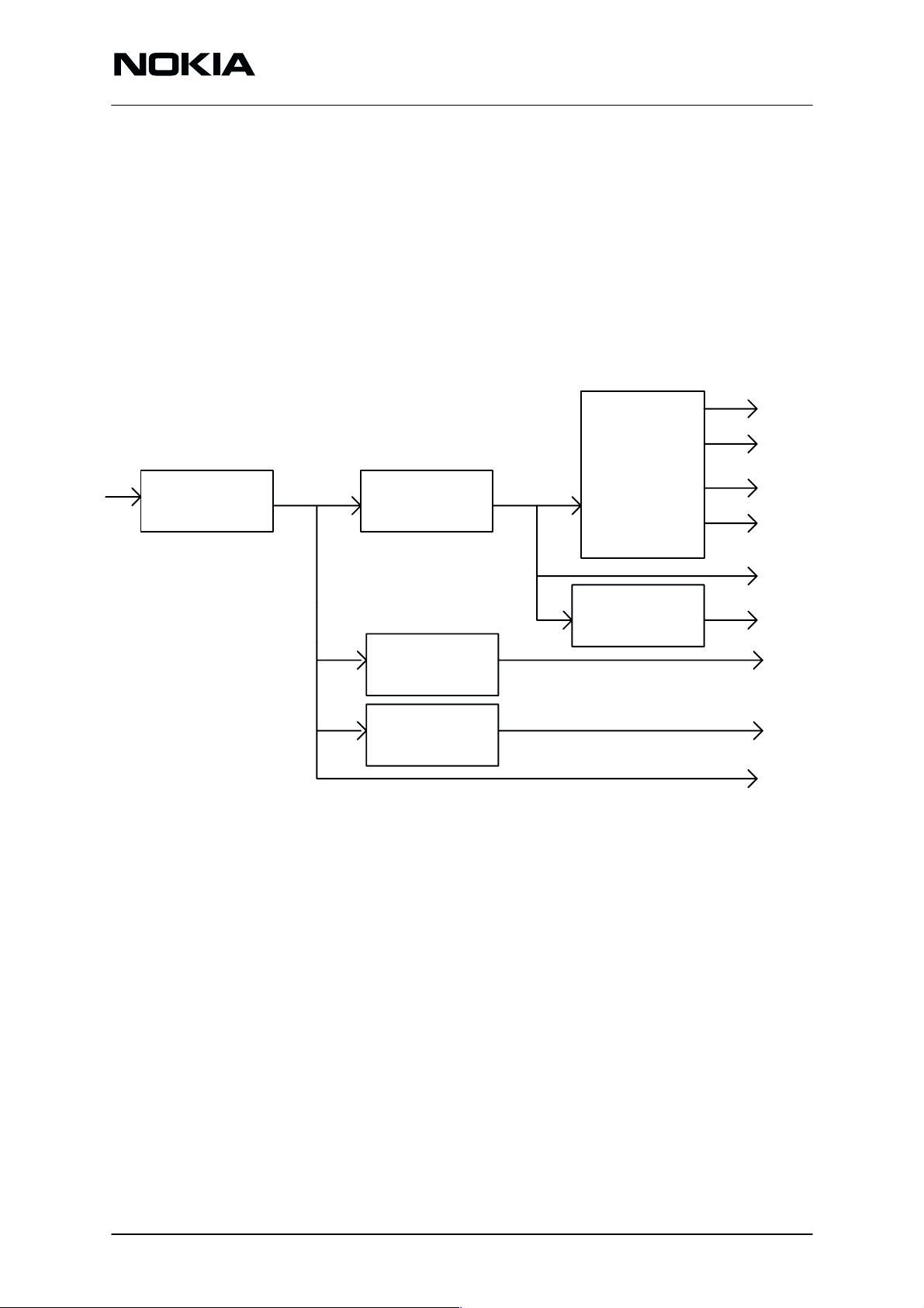
Terminal TFF–3 System Module JM1
Introduction
The Baseband module controls the internal operation of the phone. It
controls the user interface and audio interface functions. The module per-
forms all signalling towards the system and carries out audio–frequency
signal processing. The module controls the operation of the transceiver
and stores the tuning data for the phone. Also the subscriber line inter-
face between the WLL terminal and a land–line phone is performed in the
baseband module. In addition there is an immobilizer switch to detect
movement of the terminal after mounting.
System Module
All functional blocks of the baseband are mounted on a single multi layer
printed circuit board. This board contains also the RF–parts. The chassis
of the transceiver unit comprises separating walls for baseband and RF.
Components of the baseband are surface mounted, except a few. The
surface mountable components are soldered using reflow and the axial
ones manually. The connections to accessories are fed through the sys-
tem connector of the transceiver unit. There is no physical connector be-
tween the RF and baseband.
TFF-3
System Module JM1
Name of submodule Notes
CTRLU
PWRU
AUDIO
SLIC
RX
TX
SYNTH
These blocks are only functional blocks and therefore have no type nor
material codes. The circuit diagram is found in the Schematics section.
The nominal supply voltage is 13.5V. Actual supply voltage can vary
10.6V to 14.5V. The baseband and logic supply voltage is nominal 2.8V.
Control Unit for the phone
Power supply unit
Audio unit
Subscriber Line Interface module for land–line phone
Receiver
Transmitter
Synthesizer
Issue 2 02/00
E Nokia Mobile Phones Ltd.
Page 5
Page 6

TFF-3
System Module JM1
CTRLU
The control block controls all of the functions of the phone and it com-
prises the memories and the SIS–processor. An immobilizer switch is in-
cluded.
Block description
– CTRLU – PWRU
The MCU controls the watchdog timer in the PSA. It sends a positive
pulse at approximately 1 s intervals to the XPWROFF pin of the PSA to
keep the power on. If the CTRLU fails to deliver this pulse, the PSA will
remove power from the system. After the watchdog has elapsed the PSA
cuts off the supply voltages from the phone and starts again.
The flash voltage control connects programming voltage to the flash
memory and also disables the watchdog reset.
PAMS Technical Documentation
– CTRLU – AUDIO
The interface between the MCU and the MASI circuit is a bidirectional
8–bit data bus with 4 address lines. Address, data and control lines are
used in the MCU as I/O–port pins. Data lines direction must be controlled
with the MCU data direction register. Interface includes address outputs
MA0–4, data inputs (read) / outputs (write) MD0–7, chip select control
output XCS , read control output XRD, write control output XWR and in-
terrupt input XINT. When CPU is in sleep state , control signals XRD and
XCS must be in ’0’ state and address output NA0–3 and NWR in ’1’ state
and data lines ND0–7 must be in ‘0‘ state.
A valid DTMF tone is detected from interrupt line via DTMF receiver.
DTMF receiver sends the valid DTMF tone code via 4–bit bus.
– CTRLU – SLIC
The MCU sets and controls the SLIC circuit and detects actions. There is
only one landline port connected to connector.
The MCU generates the clock signal for SLIC DC/DC converter for syn-
chronization purposes.
The metering pulse is controlled by MCU for payphone usage.
– CTRLU – RECEIVER
The RX circuit power is connected on/off by RXE signal.
The received signal strength is measured over the RSSI and intermediate
frequency is measured over the IF. The LNA gain is controlled by the
AGC signal.
– CTRLU – SYNTHESIZER
The RF temperature is measured over the RFTEMP. The frequency is
controlled by the AFC signal. The synthesizer is controlled via the syn-
Page 6
E Nokia Mobile Phones Ltd.
Issue 2 02/00
Page 7
PAMS Technical Documentation
chronous serial bus SDAT/SCLK. The data is latched to the synthesizer
by the positive edge of the SLE line. The TX synthesizer power on/off
(TXSYNE) line is controlled via the PLL circuit. The 1st buffer is switched
on/of via the TXBUFF signal.
– CTRLU – TRANSMIT
The TXE line activates the power module. The power is controlled via the
TXC line which is a PWM–controlled output port.
MCU Processor
H8/2322 is a CMOS microcontroller. The CPU is ROMless version so all
memory needed is located outside the chip.
MCU operating clock (=7.3728 or 14.7456 MHz) is generated in the
MASI.
The MCU pins are listed in the table below.
NC=not connected, I=Input, O=Output, I/O=Input/Output.
TFF-3
System Module JM1
Pin number Symbol Description Pin type
1 Vcc to VL
2–5,
7–14,
16–25
6, 15, 24 Vss
26 PA5 SLIC_DET I
27 PA6 NC
28 PA7 NC
29 P67 NC
30 P66 NC
31 P65 NC
32 _IRQ0 XINT, interrupt signal from MASI I
33 Vcc to VL
34–37,
39–46,
48–51
38, 47 Vss GND
52 Vcc to VL
A0–A20 FLASH, MASI and RAM addresses
(A20, pin 25 not connected)
D0–D15 Data bus Data
Address
53 P30/TxD0 MSBUSTX, serial data to M2BUS O
54 P31/TxD1 TXBUFF O
55 P32/RxD0 MBUSRX, serial data from M2BUS I
56 P33/RxD1 FLASH_PROG, flash voltage control and PSA
watchdog disable
57 P34/SCK0 IMMO_SET, Immobilizer set signal O
58 P34/SCK1 AGC I/O
59 Vss GND
Issue 2 02/00
E Nokia Mobile Phones Ltd.
Page 7
O
Page 8
TFF-3
System Module JM1
60 P60/CS4/_DREQ0 NC I
61 P61/CS5/TEND0 NC I
62 P62/_DREQ1 ECLK, serial clock (EEPROM) I
PAMS Technical Documentation
Pin typeDescriptionSymbolPin number
63 P63/_TEND1 SISDATA,
(SIS serial data)
64 P27 SLE, synthesizer enable O
65 P26 SLIC_CLK2 SLIC gate clock for SMPS O
66 P25 MBUSRX, timeout timer start signal from M2BUS I
67 P24 SCLK serial clock for synthesizer O
68 P23 SDAT, synthesizer data O
69 P22 TXE I/O
70 P21 SIS RESET O
71 P20 RXE O
72 WDTOVF NC
73 _RES XRES reset for MCU, FLASH, MASI from PSA I
74 NMI 1 I
75 STDBY 1 I
76 Vcc to VL
77 XTAL NC
78 EXTAL CLKMCU from MASI I
79 Vss GND
I/O
80 PF7 DTMF (4) I
81 Vcc VL
82 AS NC
83 RD FLASH, MASI, SRAM Read
84 HWR MASI, SRAM Write
85 LWR FLASH Write
86 PF2 DTMF (3) I
87 PF1 DTMF (2) I
88 PF0 DTMF (1) I
89 P50/TxD2 FBUSTX O
90 P51/RxD2 FBUSRX I
91 P52/SCK2 MBUSRX for FBUS CLK I
92 P53 Serial Clock for SIS O
93 AVcc VA
94 Vref VA
95 AN0
96 AN1 VCHARSW Analog
VBATSW, not used
Analog
Page 8
E Nokia Mobile Phones Ltd.
Issue 2 02/00
Page 9
TFF-3
PAMS Technical Documentation
97 AN2 RSSI Analog
98 AN3 NC Analog
99 AN4 NC Analog
100 AN5 NC Analog
101 AN6 RFTEMP Analog
102 AN7 IMMO_DET Analog
103 AVss GND
104 Vss GND
105 P17 RING_CLK O
106 P16 TTX_CLK O
107 P15 SDA (serial data, EEPROM) I/O
108 P14 TXC O
109 P13 SEL1 O
System Module JM1
Pin typeDescriptionSymbolPin number
110–111 P12–P11 SLIC_CTRL (1–0) I/O
112 P10 XPWROFF O
113 MD0 0 (mode 4) I
114 MD1 0 (mode 4) I
115 MD2 1 (mode 4) I
116 PG0 NC
117 PG1 NC
118 PG2 RAMCS O
119 PG3 MASICS O
120 PG4 FLASHCS O
SIS MCU
AT90S2343 is a SIS (subscriber identification) circuit connected to the
controller over serial bus IIC.
Pin no. Symbol Description
1 _RESET Reset input
2 XTAL1 Clock input from MASI
4 GND GND
5 MOSI IIC bus data
7 SCL/T0 IIC bus clock
8 Vcc VSIS
EEPROM
There is one 16k EEPROMs in phone. EEPROM is a nonvolatile memory
into which is stored the tuning data for the phone.
Issue 2 02/00
E Nokia Mobile Phones Ltd.
Page 9
Page 10

TFF-3
System Module JM1
Pin no. Pin Description
4 GND GND
5 SDA IIC bus data
6 SCL IIC bus clock
8 Vcc VL
PAMS Technical Documentation
Flash memory and Flash programming
Flash memory size is 512kx16 (8MB). The Flash is a nonvolatile memory
for the program code.
Flash memory has a pre–programmed boot program. This program controls itself when the final program is stored in the memory via the FBUS
and the MBUS.
During programming only the system connector is used and the TFF–3 is
powered via the flash loading adapter (FLA–5).
RAM
The MCU has no internal memories, instead there is a SRAM circuit connected to the parallel data bus and the address bus. The size of the
SRAM is 64kB.
Immobilizer
The immobilizer uses two I/O pins of the MCU. The Output pin is used for
writing to the immobilizer and the input pin is used to read the state of the
flip–flop.
When the immobilizer is activated, the state of the flip–flop is set by the
switch and by the software via MCU output pin. After that, in the run–
time, the state of the flip–flop is read every 4 seconds. As long as the terminal stays in its original location, the state is ”1”.
When the terminal is moved, the immobilizer switch opens and causes a
state transition. After that the state of the flip–flop is found to be ”0” and
the software sets the terminal to ”terminal moved” –state. In that state
the message ”terminal moved” can be seen in the service PC software.
The operating voltage of the immobilizer (VSLIM) is obtained from the
voltage supply (VS). There is also a 0.5mAh lithium battery for backup
purpose, which is used as power supply in the situations when the terminal is not powered. This means, that the terminal can not be moved even
if it has no power. In this case the flip–flop will change its state when the
switch is opened. When the terminal is powered again the movement will
be detected.
Page 10
E Nokia Mobile Phones Ltd.
Issue 2 02/00
Page 11
PAMS Technical Documentation
PWRU
The main function of the PWRU is to feed suitable voltages in every
block. It consists of Input voltage connectors, protection circuits, separate regulators and the PSA ASIC. The PSA circuit has also another
function, the MBUS handling and watchdog.
The Power distribution diagram is below.
TFF-3
System Module JM1
PSA
VL (2.8V)
40mA
VA (2.8V)
100mA
VB
Input voltage
protection
Regulator
5V /0.5A
Regulator
3.3V 150mA
Regulator
3.3V 150mA
Regulator
8V/0.5A
to power amplifier and SLIC
The input voltage is protected against accidental interference and fault
actions. The RF –power amplifier and SLIC functions use this unregulated voltage.
Supply voltages for PSA, flash programming, SIS MCU and RF transmitter are fed from separate regulators.
VTX (2.8V)
60mA
VRX (2.8V)
50mA
VS
VSIS
VPROG
VPC
VB
10.6–14.5V
max. 2.8A
Input supply voltage
Input voltage is protected against overcurrent, overvoltage and reverse
voltage.
Also the input voltage is protected against overvoltage and reverse voltage. RF –power amplifier and SLIC functions use this unregulated voltage.
Overcurrent:
There is slow type fuse, breakdown value 5A
Overvoltage and reverse voltage:
Issue 2 02/00
E Nokia Mobile Phones Ltd.
Page 11
Page 12
TFF-3
System Module JM1
There is transient suppressor diode which work as fast Zener voltage
over 16V nom. (max. 20V). Also it work like diode in forward direction.
Also input voltage is filtered against interference from external power supply unit.
PSA
The PSA is a multi function Power Supply and charging control circuit for
Analog handportable phones. It has two separate power supplies for
baseband (VL,VA) and two externally controllable power supplies for RF
(VRX, VTX). The main functions are voltage regulators, power on/off and
charge control and reset logic (including watchdog), supply voltage and
charger detection functions and buffer for the M2BUS.
Main features of PSA:
– Voltage outputs are isolated from other regulators and from each other
– Buffer for the M2BUS
PAMS Technical Documentation
– Power on/off and reset logic
– Power off logic can be used as a watchdog
– Supply voltage monitor and automatic reset/power–off
– Battery charger detection
– Automatic on–chip current limiting
– On–chip thermal shutdown
– Surface mounted package SSOP28
PSA pinout
Control pins:
Signal Pin
number
PWRONX 22 IN PoWeR ON control input (pulled down )
VRX_ENA 2 IN VRX regulator ENAble
VTX_ENA 27 IN VTX regulator ENAble
WD_DISX 24 IN WatchDog DISable (internal pull up)
PWROFFX 23 IN Watchdog reset from MCU
PURX 16 OUT Power Up Reset signal
Type Description
Page 12
Input pins:
Signal Pin
number
VBAT1 3 Battery voltage for VRX regulator
VBAT2 11 Battery voltage for VL regulator, battery voltage monitor-
ing and internal logic
VBAT3 18 Battery voltage for VA regulator and internal analog func-
tions
E Nokia Mobile Phones Ltd.
Description
Issue 2 02/00
Page 13
PAMS Technical Documentation
TFF-3
System Module JM1
Signal
number
VBAT4 26 Battery voltage for VTX regulator
GND1 1 Ground for VRX regulator
GND2 6 Ground for internal reference voltage
GND3 12 Ground for VL regulator and internal logic
GND4 19 Ground for VA regulator and internal analog functions
GND5 28 Ground for VTX regulator
TEST 5 Test specific pin (internal pull down)
M2BUSIN 14 M2BUS data input
VCHAR 9 Divided CHARger input Voltage
DescriptionPin
Output pins:
Signal Pin
number
VA 17 Output Voltage for Analog circuitry (2.8V@100mA)
VL 13 Output Voltage for Logic circuitry (2.8V@40mA)
VRX 4 Output Voltage for RF or Analog circuitry
(2.8V@50mA)
VTX 25 Output Voltage for RF or Analog circuitry
(2.8V@60mA)
VBATSW 20 SWitched internally divided VBAT voltage
VCHARSW 8 SWitched VCHAR voltage
COSC 10 Connection for an external timing Capacitor defining
watchdog elapse time
CREF 7 Connection for an external Capacitor of the internal REF-
erence voltage
M2BUSOUT 15 M2BUS data out (open drain)
PWRONBUFF 21 inverted PWRONX state
Description
PWRONX and WD_DISX inputs have internal pull–up resistors.
M2BUSIN, VRX_ENA, VTX_ENA, TEST and PWROFFX inputs have in-
ternal pull–down resistors.
Functional descriptions
PSA
The linear regulators are high performance regulators. Regulators have
internal current limiting. All the regulators have low quiescent currents
thus extending the battery life.
VA and VL are intended for baseband circuits, VRX and VTX for RF circuitry.
Voltage monitor
This function is used to monitor VBAT voltage level. The threshold level
is set by internal resistor divider.
Issue 2 02/00
E Nokia Mobile Phones Ltd.
Page 13
Page 14
TFF-3
System Module JM1
The circuit monitors the voltage at the VBAT input and forces the circuit to
Reset if the voltage level is below allowed limit voltage, VBATcoff–. A
hysteresis is included to prevent oscillation between different states.
Thermal protection
Thermal shutdown protects PSA from overheating. Thermal shutdown includes hysteresis in order to prevent oscillation during the thermal protection.
Power supply voltage detection
Thermal shutdown protects PSA from overheating. Thermal shutdown includes hysteresis in order to prevent oscillation during the thermal protection.
M2BUS buffer
M2BUS is a serial bus between mobile and accessories.
M2BUS baud rate is 9600 bps.
PAMS Technical Documentation
The buffer translates the logical input signal to open–drain output.
Rgw M2BUS buffer thruth table is below.
Separate regulators
Separate supply voltages:
– Regulator 5V is for PSA and some RF purposes.
– Regulator 8V is used for RF TX buffers
– Regulator 3.3V is used for flash programming
– Regulator 3.3V is used for SIS MCU
Input Output
LOW LOW
HIGH Z
Page 14
E Nokia Mobile Phones Ltd.
Issue 2 02/00
Page 15

PAMS Technical Documentation
AUDIO
The Audio block includes the MASI ASIC, the DTMF circuitry and the
SYSTEM connector.
MASI ASIC
MASI is a single chip audio/signalling processor in a 64 TQFP package
for the NMT450 system.
Main features
– Low power consumption modes
– 8 bit parallel interface with pull ups
– FM demodulator
TFF-3
System Module JM1
FFSK modem features
– Full duplex 1200 baud signalling
– FSK indicator and level detector
– FII filter and gain control
– DMS facility
Audio features
– Low noise microphone amplifier
– Input for a handset microphone or an accessory
– Microphone sensitivity compensation +24/–7 dB range (5 bits)
– Compander
– RX and TX filters
– Tx hard limiter
– Tx AGC
– Transmitter compensation amplifier with +1.875/–1.875 dB range (4
bits)
– Compensation amplifier for different RX deviations with +7.5/0 dB
range (4 bits)
– Volume control amplifier with –20/+17.5 range (4 bits)
– Earphone amplifier with drive capability for ceramic earpiece
– Buffered output for a handset or an accessory
– Mute switches
– Speech scrambler and descrambler
Other features
– Dual and single tone multifrequency generator
– IF counter
– 8 bit general purpose DAC
– Programmable output clocks with clock stop for MCU, LCD and SIS
– Two external interrupt sources
– Programmable timer
– Summing stage for voice/data, signalling and fii
Issue 2 02/00
E Nokia Mobile Phones Ltd.
Page 15
Page 16
TFF-3
System Module JM1
PAMS Technical Documentation
MASI Pinout
Pin no Symbol Pin type Notes
1 VDD1 PWR +2.7 ... 3.5 V Supply voltage for digital part
2 XCS DIN/pd Chip select signal, active state LOW, pull–down > 50 kW
3 A4 DIN/pu 5–bit address bus, MSB, pull–up > 50 kW
4 A3 DIN/pu 5–bit address bus, pull–up > 50 kW
5 A2 DIN/pu 5–bit address bus, pull–up > 50 kW
6 A1 DIN/pu 5–bit address bus, pull–up > 50 kW
7 A0 DIN/pu 5–bit address bus, LSB, pull–up > 50 kW
8 D7 DIO 8–bit bidirectional data bus MSB
9 D6 DIO 8–bit bidirectional data bus
10 D5 DIO 8–bit bidirectional data bus
11 D4 DIO 8–bit bidirectional data bus
12 D3 DIO 8–bit bidirectional data bus
13 D2 DIO 8–bit bidirectional data bus
14 D1 DIO 8–bit bidirectional data bus
15 D0 DIO 8–bit bidirectional data bus LSB
16 NMI DOUT Non maskable Interrupt request
17 VSS1 PWR 0 V Supply voltage, ground for digital part
18 XCLR DIN HW reset input, active state LOW
19 TMODE DIN/pd Test mode selection, pull–down > 50 kW
20 TSEL DIN/pd Scan test selection, pull–down > 50 kW
21 XINT DOUT Interrupt request to MCU, active state LOW
22 EXTINT1 DIN External interrupt request, falling edge active (note: this pin
is test scan select when TMODE is high)
23 EXTINT2 DIN External interrupt request, falling edge active
24 VDD2 PWR +2.7 ... 3.5 V Supply voltage for digital in Analog part
25 IF AIN IF input
26 DAF AIN Audio input
27 FILO AOUT Rxfilter output
28 EXPI AIN Expander/Descrambler input
29 EXPO AOUT Expander/Descrambler output
30 VOLI AIN Volume control amplifier input
31 VSA1 PWR 0 V Supply voltage, ground for RX Analog
(including EARAMP & EXTEAR)
32 EXTEAR AOUT Buffered output for handset or an accessory
33 EARP AOUT Earphone driver output, positive
34 VDA1 PWR + 2.7 ... 3.5 V Supply voltage for RX Analog
(including EARAMP & EXTEAR)
Page 16
E Nokia Mobile Phones Ltd.
Issue 2 02/00
Page 17
PAMS Technical Documentation
NotesPin typeSymbolPin no
35 EARN AOUT Earphone driver output, negative
36 DACO AOUT DA converter output
37 CALLCNT AIN Voltage sensor input for battery change during call
38 REF AOUT Internal analog signal ground, stabilization capacitor
39 ATOUT AOUT Analog test circuit output
40 MIC AIN Microphone amplifier input,
41 BIMIC AOUT Microphone bias output
42 CMIC AIN Microphone bias current stabilizing capacitor
43 EXTMIC AIN Audio input for a handset or an accessory
44 TXPBO AOUT Transmit bandpass filter (scrambler) output
45 COMI AIN Compressor input
46 MOD AOUT transmit path output
47 ATST AOUT Analog test output
System Module JM1
TFF-3
48 VDA2 PWR + 2.7 ... 3.5 V Supply voltage for TX Analog & NVSGEN
49 NSV AOUT Negative supply voltage, –7V output
50 NSV2 AOUT negative supply voltage –4.66V, for external capacitor
51 NSV1 AOUT negative supply voltage –2.33V, for external capacitor
52 NCPP AOUT Negative supply charge pump (external) capacitor positive
53 NCPN AOUT Negative supply charge pump (external) capacitor negative
54 VSA2 PWR 0 V Supply voltage, ground for TX Analog & NVSGEN
55 TOUT DOUT Test scan data output
56 CLKIN CIN 14.7456 MHz crystal oscillator input or input for the external
clock
57 CLKOUT COUT 14.7456 MHz crystal oscillator output
58 VSS2 PWR 0 V Supply voltage,
ground for digital in Analog part & Buzzer
59 BUZZ AOUT Buzzer output, open collector
60 CLKLCD DOUT Clock signal for LCD, 230.4 kHz, 57.6 kHz or 14.4 kHz
61 CLKSIS DOUT Clock signal for SIS processor, 3.6864MHz or 7.3728MHz
62 CLKMCU DOUT Clock signal for MCU, 3.6864 MHz, 7.3728 MHz or 14.7456
MHz
63 XWR DIN/pu Write control signal, active state LOW, pull–up > 50 kW
64 XRD DIN/pd Read control signal, active state LOW, pull–down > 50 kW
Issue 2 02/00
E Nokia Mobile Phones Ltd.
Page 17
Page 18
TFF-3
System Module JM1
PAMS Technical Documentation
SLIC block
The TFF–3 line adapter hardware is implemented using the STLC3065
SLIC custom–designed for wireless applications. The pins of the
STLC3065 are listed below.
Pin no Symbol Pin type Notes
1 D0 I Control interface,input bit 0
2 D1 I Control interface,input bit 1
3 D2 I Control interface,input bit 2
4 P1 I Control interface, port selection bit
5 P2 I Control interface, port selection bit
6 _DET1 O Logic interface output of the line port 1 detector, open drain
7 _DET2 O Logic interface output of the line port 2 detector, open drain
8 _DET O Logic interface output of the supervision line detector, open
drain
9 CKTTX I Metering pulse clock input
10 CTTX1 Metering burst shaping external capacitor
11 CTTX2 Metering burst shaping external capacitor
12 RTTX O Metering pulse cancellation buffer output
13 FTTX O Metering pulse buffer
14 RX I 4 wire input port (RX input)
15 ZAC1 O RX buffer output
16 ZAC I AC impedance synthesis
17 RS Protection resistor image
18 ZB Balance network for 2 to 4 wire conversion
19 CAC I AC feedback input
20 TX O 4 wire output (TX output)
21 VF I Feedback input for DC/DC converter controller
22 CLK I Power switch controller clock
23 GATE O Driver for external PowerMOSFET
24 RSENSE I Voltage input for current sensing
25 VPOS I Positive supply input voltage
26 CVCC Internal positive voltage supply filter
27 AGND Analog ground
28 RLIM I Constant current feed programming pin.
29 IREF I Internal bias current setting pin
30 RTH I Off–hook threshold programming pin
31 RD I DC feedback and ring trip input
Page 18
E Nokia Mobile Phones Ltd.
Issue 2 02/00
Page 19
TFF-3
PAMS Technical Documentation
NotesPin typeSymbolPin no
32Imm ILTF O Transversal line current image output
33 CSVR Battery supply filter capacitor
34 BGND Battery ground
35 VBAT Regulated battery voltage self generated
36 RING2 2 wire port 2, RING wire (Ib is the current sunk into this pin)
37 RING1 2 wire port 1, RING wire (Ib is the current sunk into this pin)
38 NC
39 NC
40 NC
41 TIP1 2 wire port 1, TIP wire (Ia is the current source from this pin)
42 TIP2 2 wire port 2, TIP wire (Ia is the current source from this pin)
43 CREV Reverse polarity transition time control
44 VBAT1 Frame connection
System Module JM1
Issue 2 02/00
E Nokia Mobile Phones Ltd.
Page 19
Page 20

TFF-3
System Module JM1
Immobilizer
The immobilizer uses two I/O pins of MCU. Output pin is used for writing
to the immobilizer and from input pin the state of the flip–flop can be read.
When the immobilizer is activated, the state of the flip–flop is set by the
switch and by the software via MCU output pin. After that, in the run–time,
the state of the flip–flop is read every 4 seconds. As long as the terminal
stays in its original location, the state is ”1”.
When the terminal is moved, the immobilizer switch opens and causes a
state transition. After that the state of the flip–flop is found to be ”0” and
the software sets the terminal to ”terminal moved” –state. In that state the
message ”terminal moved” can be seen in the service PC software.
PAMS Technical Documentation
Vs
Immo_set
Battery charging
The operating voltage (VSLIM) of the immobilizer is obtained from the
voltage supply (VS). There is also a 0.5mAh lithium battery for backup
purpose, which is used as power supply in the situations when the terminal is not powered. This means, that the terminal can not be moved even
if it has no power. In this case the flip–flop will change its state when the
switch is opened. When the terminal is powered again the movement will
be detected.
Immobilizer circuitry below:
&
&
&
&
Immo_det
Page 20
3.3V
E Nokia Mobile Phones Ltd.
Issue 2 02/00
Page 21

PAMS Technical Documentation
RF Module
Introduction
The RF module is designed for a WLL cellular phone which operates in
the NMT–450i system. The purpose of the module is to receive and demodulate the radio frequency signal from base station and to transmit
modulated RF signal to base station.
The modulation method used in the phone is FM modulation (F3E).
Rx module
Tx module
Synthesizer module
TFF-3
System Module JM1
Name of submodule
RX
SYNT
TX
All submodules are only functional blocks, They are constructed on same
PCB and have no material codes by themselves.
The RX module receives and demodulates the radio frequency signal from
the base station.
The transmitter synthesizer generates a frequency modulated RF signal for
the transmitter section. The transmission frequency is generated by a
phase–locked loop (PLL). The synthesizer circuit contains VCO, synthesizer
logic and loop filter.
The receiver synthesizer generates the first injection frequency to the receiver module. The local frequency is generated by a phase–locked loop
as in transmitter synthesizer. The synthesizer circuit contains VCO, synthesizer logic and loop filter.
The Transmitter module generates and amplifies the RF signal to be transmitted to the base station.
Issue 2 02/00
E Nokia Mobile Phones Ltd.
Page 21
Page 22

TFF-3
System Module JM1
Technical Specifications
Maximum ratings
The maximum power supply voltage during transmission must not exceed 17 V. Higher power supply voltages may destroy the power amplifier module.
Parameter Value
Power Supply max.VB 14.5 V
PAMS Technical Documentation
Switched mode power supply with regulated output
Regulated supply voltage, VPC 8.0 V
Regulated supply voltage, VS 5.0 V
Regulated supply voltages VRX, VTX 2.82 V +/– 5 %
Operating temperature range –25 ... +55 ° C
13.5 V
Control Signals
In the following table the RF current consumption can be seen in different
modes.
control signals
RXE TXSYNE TXBUFF TXE
H H H H 2200–2800
H H H L 200 RX on, TX–synthe-
H H L L 160 RX on, TX–synthe-
H L L L 150 RX on
current consump- Notes
tion (mA)
power level 2
1300–1500
600–800
power level 1
power level 0
sizer on, TX–buffer
on
sizer on
L L L L 120 all RF parts pow-
ered down
The current consumption of different RF parts can be seen in the following block diagram.
Page 22
E Nokia Mobile Phones Ltd.
Issue 2 02/00
Page 23

PAMS Technical Documentation
Power consumption Diagram
TFF-3
System Module JM1
AGC
VS
regulator
5.0V
VRX
regulator
2.82 V
VA
regulator
2.82 V
20 mA
2 mA
3 mA
9 mA
15 mA
9 mA
LNA
IF amplifier
IF circuit
LO buffer
RX–VCO
Synthesizer IC
TXE
TXBUFF
Battery
13.3V
Battery
TXSYNE
regulator
2.82V
VTX
regulator
8.0V
VPC
2 mA
15 mA
40 mA
100 mA–
250 mA
400 mA–
2400 mA
VCTCXO
TX–VCO
1st
TX Buffer
TX power
control
and
2nd
TC Buffer
PA
Block diagram of Radio sub–module
Issue 2 02/00
E Nokia Mobile Phones Ltd.
Page 23
Page 24

TFF-3
System Module JM1
PAMS Technical Documentation
450 kHz FILTER
RSSI
IF CIRCUIT
IF
PHASE SHIFTER
UMA 1015
SYNTHESIZER IC
TANK CIRCUIT FOR 2.ND LO
1ST TX BUFFER
TX VCO
PLL
PLL
LOOP FILTER
MOD
SLE
SCLK
SDATA
AGC
TXBUFF
AFC
TXC
VCTCXO 14.85 MHz
TXE
REGULATOR
VS
REGULATOR
VRX
REGULATOR
8.0V
VPC
VBAT
5.0V
2.82 V
2ND TX BUFFER
RXE
REGULATOR
VTX
2.82 V
TXSYNE
IF AMPLIFIER
45 MHz
CRYSTAL FILTER
DIODE MIXER
RX–FILTER
LNA
ANTENNA
LOOP FILTER
RX LO BUFFER
DUPLEX–FILTER
RX VCO
AMPLIFIER MODULE
VA
TX POWER CONTROL
POWER DETECTOR
DIR_COUPLER
Page 24
E Nokia Mobile Phones Ltd.
Issue 2 02/00
Page 25

PAMS Technical Documentation
Connections
Connections to Baseband sub–module
TFF-3
System Module JM1
Signal
Name
AFC Analog in The reference oscillator frequency adjust.
IF Analog out 2nd IF signal
MOD Analog in Modulation signal for transmitter (Audio + data)
RFTEMP Analog out RF temperature, which is determined by NTC resistor.
RSSI Analog out Received signal strength indicator. Voltage measurement.
SCLK Digital in Serial clock for synthesizer. Active state: Rising edge
SDAT Digital in Serial data for synthesizer. Active state: High
SLE Digital in Synthesizer enable. Active state: High
TXBUFF Digital in 1st TX buffer on/off. High when on.
TXE Digital in Transmitter on/off. High when on.
TXSYNE Analog out TX synthesizer power control
VB Power Battery voltage
VA Power Regulated voltage for synthesizer IC
VRX Power Regulated voltage for receiver & receiver synth
VTX Power Regulated voltage for transmitter synth
VS Power Regulated voltage for receiver LNA
Type Function
VPC Power Regulated voltage for 1 st. TX buffer and Power control
AGC Digital in RX low noise amp. gain control
Function Digital Control Signal name Value
Supply voltage VDD 2.82 V
Logical 1 VOH VDD*0,7...VDD+0.3V
Logical 0 VOL –0.3V...VDD*0,3
Logical 1 IOH <5mA
Logical 0 IOL <5mA
CLKIN 14.85 MHz VCTCXO signal Value
Level 1 Vpp min
Load impedance 10 k W\\10pF +/– 10%
Start time < 60 mS after Vref rising
Issue 2 02/00
E Nokia Mobile Phones Ltd.
Page 25
Page 26

TFF-3
System Module JM1
AFC VCTCXO control voltage
Type analog signal (DC–level)
Level 0.1...2.7 V DC
Load impedance ZL > 10 kW
Control step size < 12 mV
IF 450 kHz 2nd IF signal
Level 300 mVp–p (typical) not speci-
Source impedance < 1.0 kW
MOD Modulation signal MOD for
transmitter (Audio + data)
Type Analog signal
Nominal level 300 mVrms @3.0 kHz deviation
PAMS Technical Documentation
fied by manufacturer
Load impedance ZL > 22 kW
RSSI Received signal RSSI
strength indicator
DC–level 0,5...1.6 V (–115...–45 dBm)
dynamic range 70 dB
Source impedance 56 kW
SCLK Serial clock for synthesizer
Type digital signal
Pulse width > 1 us
SDAT Serial data for synthesizer
Type digital signal
Pulse width > 1 us
VALUES
Control byte xx100 000x x10000xx
(synte_initial_const)
Reference divider 1188 (25 kHz channel)
Divider formulas for
TX oscillator
Divider formulas for
RX oscillator
SLE Synthesizer enable
Type Digital signal
Function 0 = synthesizer enabled
Page 26
E Nokia Mobile Phones Ltd.
N = 2*ch +36238
(TX_synte_base_const1 8D,8E)
N = 2*ch +33438
(RX_synte_base_const1 82,9E)
1 = synthesizer disabled
Issue 2 02/00
Page 27

TFF-3
PAMS Technical Documentation
RXE Receiver enable
Type Digital signal
Function 0 = Receiver off
1 = Receiver on
On–state current < 100 uA
AGC Automatic Gain Control
Type Digital signal
Function 0 = Gain high
1 = Gain low
On–state current < 100 uA
TXC Transmitter power control
Type PWM signal
Function Duty cycle of the TXC signal
defines the TX power level.
PWM frequency 14 kHz (7.2 kHz)
System Module JM1
Level 0...3.3 V DC
Number of duty cycle steps 256
Load impedance > 100 kohm
TXBUFF Transmitter on/off control
Type Digital signal
Function 0 = TX off
1 = TX on
TXE Transmitter on/off control
Type Digital signal
Function 0 = TX off
1 = TX on
VBAT Battery voltage
Nominal value 13.5 V
Minimum value 10.6 V
Absolute maximum 14.5 V
Max. input current 3.4 A
Key RF components
Name Manufacturer Type NMP code
Antenna ALGON G1–U1/NN1.HH 0660064
Duplexer LK–Products Q8–A9/NP1 4508216
Saw filter Hitachi HWAB219 4510135
Issue 2 02/00
E Nokia Mobile Phones Ltd.
Page 27
Page 28

TFF-3
System Module JM1
45 MHz IF filter KDS DSF753SB 4510085
PAMS Technical Documentation
NMP codeTypeManufacturerName
450 kHz IF filter NTK / Kyocera MLF–Q–type,
PBFC450R12DR
IF circuit Toshiba TA31136F 4349694
VCTCXO KDS DTO–432H1 4510171
PLL IC Philips UMA1015AM 4340393
RX VCO Alps URAY8XR02A 4350169
TX VCO Alps URAY8XT02A 4350167
Power amplifier Mitsubishi M57704L 4352537
455P005
Antenna
Phone uses a fixed antenna. The electrical length of antenna is 1/2 wave
length.
Receiver
The receiver is a dual–conversion superheterodyne using two intermediate frequencies, 45 MHz and 450 kHz.
The RF signal from the duplexer RX port is applied to the low noise RF
amplifier. The amplifier is realized with transistor V910. Amplifier stage
input matching is accomplished by C903 and L901. R901 and R924 are
used for biasing. Output matching is carried out by L911. C902 and C912
are used for RF bypassing. Stability is ensured with serial connection of
R913 and C901 to the ground.
Next the signal is filtered with Z930. The filter is followed by a single balanced diode mixer, comprising Z931, Z932, Z950 and V930.
After the mixer the 45 MHz IF signal is filtered with crystal filter Z940. The
matching between mixer and the filter comprises L940, R940 and C940.
After that the IF signal is amplified by V960. Input matching is performed
by L980 and L981. The biasing elements comprise R960, R961, R962
and R963. Output matching elements comprise L961. Capacitors C960
and C962 are used for RF bypassing.
The second mixer, IF amplifier and quadrature detector are all integrated
in the circuit N970. The second LO frequency, 44.55 MHz, is the third
harmonic of the VCTCXO frequency. LO signal is realized with tank circuit
C972 and L971. After the mixer the 450kHz IF signal is filtered with ceramic filter Z970. The IF amplifier output signal is phase shifted by resonance circuit C977, R971 and L970. After this the signal is rectified to
square wave.
The RSSI and 2nd IF signal (450 kHz) are fed to the audio/logic unit.
RX Synthesizer
The first injection frequency is generated by a digital phase locked loop
(PLL). The PLL consists of a VCO, a loop filter and a PLL IC which in-
Page 28
E Nokia Mobile Phones Ltd.
Issue 2 02/00
Page 29

PAMS Technical Documentation
cludes reference and main dividers. The output frequency of the loop
(LO) is obtained from a voltage–controlled oscillator (VCO) G520. The
output level of VCO is 0 dBm +/– 2 dB. The VCO output signal is amplified by transistor V950 and fed to the receiver mixer via Z950. A portion
of output signal is fed back to the synthesizer.
The overall divisor of the chain is selected according to the desired channel.
The internal dividers of N400 are programmed with 17 bits, which are
transferred serially on the SDATA (synthesizer data) line from the processor into an internal shift register also located in N400. Data transfer is
timed with SCLK clock pulses.
The divided frequency is compared with a highly stable reference frequency from VCTCXO by a phase comparator in the PLL circuit (N400).
The phase comparator controls the VCO frequency by means of a DC
voltage through the loop filter so as to keep the divided frequency applied
to the phase comparator equal to the fixed reference frequency.
TFF-3
System Module JM1
The reference frequency is 12.5 kHz. This reference frequency is obtained from voltage controlled temperature compensated crystal oscillator
(VCTCXO). Oscillator frequency is 14.85 MHz. The VCTCXO frequency is
divided by 1188.
RX loop filter
The Phase comparator output is pin 3. If the VCO frequency is too high,
the output goes low and discharge integrator capacitor C421. After this,
the DC control voltage and the VCO frequency will decrease.
If the VCO frequency is too low, the output goes high and charge the integrator capacitor C421. Thereafter the DC control voltage and the VCO
frequency will go up.
Output pulses from the phase detector have to be supplied to the loop filter. The function of the integrator is to convert positive and negative
pulses to DC voltage. The remaining ripple and AC components are filtered in the three stage lowpass filter.
TX Synthesizer
The transmitter synthesizer generates a frequency modulated transmitter
signal to the transmitter section. The injection frequency for the transmitter is generated by a digital phase locked loop (PLL). The modulated TX
frequency is generated in the TX–VCO (G420). Output level of the VCO is
0 dBm +/– 2 dB. After VCO, the TX signal is amplified in the 1st TX buffer
V440 before the 2nd TX buffer V610 and power amplifier module. Gain in
the 1st TX buffer is about 14 dB. Gain in 2nd TX buffer is controlled with
variation of supply voltage coming from power control circuit.
TX Loop Filter
Output pulses from the phase detector N400 pin 17 are supplied to the
loop filter. The integrator, which is constituted of R433, C435 and C436,
Issue 2 02/00
E Nokia Mobile Phones Ltd.
Page 29
Page 30

TFF-3
System Module JM1
converts positive and negative pulses to DC voltage. The remaining ripple
is filtered in the three stage low–pass filter.
Transmitter
The transmitter is basing on the power amplifier module (N620). The
modulated RF signal from the TX synthesizer is applied to the 50 ohm input of the transmitter module. T he power level is controlled by the voltage which is supplied to pin 2 of PA module and pin 4 of V610 (2nd TX
buffer’s supply voltage). A voltage proportional to the output power is rectified from a coupler strip by DC–biased Schottky diode V640. This rectified voltage is fed to a differential amplifier which consists of transistor
V631 and V632 .
The reference voltage to control PA module is filtered from the PWM signal TXC to DC voltage by two stage lowpass filter. The differential amplifier adjusts the source voltage of the transistor V630 so that the reference
voltage and the voltage proportional to the output power are equal. The
transmitter is switched on when TXE goes high (logic 1), which enables
the transmitter power control circuit by transistor V633 . When the transmitter is inactive (TXE low) the RF level from the transmitter is reduced
below –57 dBm.
PAMS Technical Documentation
Page 30
E Nokia Mobile Phones Ltd.
Issue 2 02/00
Page 31

PAMS Technical Documentation
RF Characteristics
Temperature range
TFF-3
System Module JM1
Line Symbol Minimum Typical /
Nominal
Operating temperature –25 +55 °C
Maximum Unit / Notes
Duplexer specification
Transmitter Receiver
Frequency 452.5...457.5 MHz 462.5...467.5 MHz
Insertion loss max 2.2 dB 4.8 dB
Ripple at BW max 1.0 dB 2.0 dB
Termination impedance 50 W 50 W
Permissible input power 25 W 1 W
V.S.W.R. at BW 1.6 max. 1.6 max.
Attenuation min
Frequency
[MHz]
462.5...467.5 65 452.5 ...457.5 65
905 ...915 40
1357 ...1373 40
Att. [dB] Frequency
[MHz]
Att. [dB]
1810 ...1830 40
RX submodule specifications
N=Normal
E=Extreme
conditions
Frequency range 462.500...467.475 MHz
Type FM receiver, 2 IFs
Intermediate Frequencies 45 MHz, 450 kHz
N RF–sensitivity < –113 dBm (SINAD 20 dB)
E RF–sensitivity < –110 dBm (SINAD 20 dB)
N Adjacent channel selectivity > 67 dB (25 kHz)
E Adjacent channel selectivity > 60 dB (25 kHz)
N Spurious response rejection > 67 dB
N Intermodulation rejection > 67 dB
Blocking :
Parameter Unit / Notes
Issue 2 02/00
E Nokia Mobile Phones Ltd.
Page 31
Page 32

TFF-3
System Module JM1
E=Extreme
conditions
PAMS Technical Documentation
Unit / NotesParameterN=Normal
N RX–band excluding the receiver freq. ±
10 MHz
N Spurious emissions
N 100 kHz ... 1000 MHz < –57 dBm
N 1000 MHz ... 4000 MHz < –47 dBm
N / E Audio harmonic distortion < 5 % (third harmonic)
N / E Noise & hum < –35 dB
N / E RSSI dynamic range > 65 dB
N / E AGC attenuation 5...10 dB
> –80dB
Preamplifier
Minimum Typical /
Nominal
Supply voltage 5.0 V
Frequency band 462.5 467,475 MHz
Current consumption (AGC off) 18 20 mA
Current consumption (AGC on) 7 - 9 mA
Insertion gain (AGC off) 19 22 dB
Maximum Unit / Notes
Insertion gain (AGC on) 10 dB
Gain flatness ±1 dB
Noise figure 1.6 1.8 dB
Reverse isolation 30 40 dB
IIP3 –5 dBm
Input return loss (Z0=50W) –4 dB
Output return loss (Z0=50W) –11 dB
RX–filter
Minimum Typical /
Nominal
Center frequency, f
Bandwidth (–0,8 dB) ±3 MHz
Stopband attenuation
f0 -10 MHz
f0 -90 MHz
Insertion loss 3,7 4 dB
0
12
45
464,5 MHz
15 dB
50 dB
Maximum Unit / Notes
Passband ripple 0,7 1,0 dB
Terminating impedance 50W // 18nH
Page 32
E Nokia Mobile Phones Ltd.
Issue 2 02/00
Page 33

PAMS Technical Documentation
1st mixer
TFF-3
System Module JM1
Minimum Typical /
Nominal
Frequency band
RF 462.500 467.475 MHz
LO 417.500 422.475 MHz
IF 45 MHz
Conversion loss 6 8 dB
IIP3 12 dBm
IIP2 18 dBm
LO power level 0 dBm
LO–RF isolation 30 dB
Maximum Unit / Notes
1st IF–filter
Minimum Typical / Nomi-
nal
Type Crystal 4–pole
Center frequency, f
Operating temperature –25 +85 °C
0
45.000 MHz
Maximum Unit / Notes
3dB bandwidth ± 7,5 kHz Passband
Stopband attenuation
fo ± 22 kHz 25 dB adj channel
fo -900 kHz ± 10 kHz 80 dB 2nd mirror
Spurious response rejec-
tion
fo±150 ... ±1000 kHz
Insertion loss 3 dB
Passband ripple 1 dB
Terminating impedance 600 // 2 W // pF
Group delay distortion 30 ms at f0 ± 5 kHz
40 dB
IF–amplifier
Minimum Typical /
Nominal
Operating frequency 45 MHz
Supply voltage 2.82 V
Maximum Unit / Notes
Input impedance 800 // 1.5 W // pF
Output impedance 1000 W
Issue 2 02/00
E Nokia Mobile Phones Ltd.
Page 33
Page 34

TFF-3
System Module JM1
PAMS Technical Documentation
Minimum
Nominal
Insertion gain 15 18 dB
Noise figure 3 dB
IIP3 –30 dBm
2nd IF–filter
Minimum Typical /
Nominal
Center frequency 450 kHz
Temperature range +10 (–30) +50 (+70) °C
6 dB bandwidth ± 6.0 (5,5) kHz
26 dB bandwidth ± 9.0 (10,0) kHz
50 dB bandwidth ± 12,5 (13,0) kHz
Insertion loss 5,0 (6,0) dB
Ripple 3,0 (4,0) dB
Stopband attenuation
Maximum Unit / Notes
Unit / NotesMaximumTypical /
f0 ±13 ... 25 kHz
f0 ±25 ... 100
kHz
Spurious response re-
jection 0,1...1MHz
Group delay time 100 (120) ms at f0 ±4 kHz
Input & output imped-
ance
40
35
20 dB
1,35 1,5 1,65 kW
dB
dB
IF–circuit
Minimum Typical /
Nominal
Supply voltage 2.82 V
Current consumption 2,0 mA
2. lo frequency 44.550 MHz
RSSI dynamic range 70 dB
Case 16 SSOP
Maximum Unit / Notes
Page 34
E Nokia Mobile Phones Ltd.
Issue 2 02/00
Page 35

PAMS Technical Documentation
TX submodule specification
Power amplifier
TFF-3
System Module JM1
Minimum Typical /
Nominal
Supply voltage 13.5 17 V
Current consumption 2.8A mA (at P
Input power 26 dBm
Output power 38.5 dBm (7W)
Efficiency 35 40 % (at operation point)
Harmonic level –30 dB (at 2*f
Harmonic level dB (at 3*f
Input VSWR 2.8
Output VSWR No degradation or de-
Output VSWR No parasitic oscillation
Maximum Unit / Notes
= 7W)
out
)
carrier
and hig-
her)
stroy
carrier
Power control and 2nd TX buffer
Minimum Typical /
Nominal
Supply voltage 8,0 V
Maximum Unit / Notes
Drive current 70 150 250 mA
Power control range 20 24 dB
Control step size 0.2 dB
Coupler lines
Minimum Typical /
Nominal
Frequency range 403 520 MHz
Coupling coefficient 18 20 22 dB
VSWR input (Z0=50W) 1:1.2
Isolation 15 dB (with 50 ohm in/out)
Insertion loss 0.25 dB (with 50 ohm in/out)
Maximum Unit / Notes
Issue 2 02/00
E Nokia Mobile Phones Ltd.
Page 35
Page 36

TFF-3
System Module JM1
Synthesizer submodule specifications
PLL
PAMS Technical Documentation
Minimum Typical /
Nominal
Frequency band 400 1100 MHz
Channel separation 25 kHz
Supply voltage 2.6 2.82 5,5 V
Current consumption 9,0 mA
Maximum Unit / Notes
RX VCO
Minimum Typical /
Nominal
Frequency band 416.000 425.000 MHz
Operating temperature –30 +80
Output level –2,5 0 +2,5 dBm / 50 W
Harmonic attenuation 12 dB (2nd)
Frequency pulling
due to load
variations
due to supply
voltage
Supply voltage 2.7 2.82 3.0 V
Maximum Unit / Notes
o
C
± 200 kHz (VSWR = 2.0)
± 100 kHz (Vcc ± 0.5 V)
Current consumption 12 15 mA
SSB phase noise –118 dBc/Hz (20 kHz offset,
1Hz BW)
Control Voltage 1.75 4.75
SNR without vibration –44 dB (± 3 kHz dev at
1kHz)
SNR with vibration –34 dB (± 3 kHz dev at
1kHz, at 55 to 150 Hz,
for 15 m/s
tion)
2
accelera-
TX VCO
Minimum Typical /
Nominal
Frequency band 450.000 460.000 MHz
Operating temperature –30 +80
Output level –2,5 0 +2,5 dBm / 50 W
Harmonic attenuation 12 dB (2nd)
Maximum Unit / Notes
o
C
Page 36
E Nokia Mobile Phones Ltd.
Issue 2 02/00
Page 37

PAMS Technical Documentation
TFF-3
System Module JM1
Minimum
Nominal
Frequency pulling
due to load
variations
due to supply
voltage
Modulation
mod. sensitivity 48 49,5 51 dBmV (±1.5 kHz dev
Supply voltage 2.7 2.82 3.0 V
Current consumption 12 15 mA
SSB phase noise –116 dBc/Hz (20 kHz offset,
SNR without vibration –44 dB (± 3 kHz dev at
SNR with vibration –34 dB (± 3 kHz dev at
±200 kHz (VSWR = 2.0)
± 100 kHz (Vcc ± 0.5 V)
Unit / NotesMaximumTypical /
at 1 kHz)
1Hz BW)
1kHz)
1kHz, at 55 to 150 Hz,
for 15 m/s
tion)
2
accelera-
Isolation amplifier (1st TX buffer)
Minimum Typical /
Nominal
Frequency range 410 490 MHz
Input power –1 0 +1 dBm
Output power 13 14 15 dBm
Reverse isolation 30 dB
Supply voltage 8,0 V
Current consumption 40 mA
Maximum Unit / Notes
VCTCXO
Minimum Typical /
Nominal
Frequency 14,85 MHz
Control voltage 0.3 3,0 V
Maximum Unit / Notes
frequency accuracy ± 2.5 ppm
Output level 1 Vpp AC
Supply voltage 2.82 V
Current consumption 2 mA
Issue 2 02/00
E Nokia Mobile Phones Ltd.
Page 37
Page 38

TFF-3
System Module JM1
PAMS Technical Documentation
Parts list of WN1 Basic Module
(EDMS Issue 3.3) Code: 0201416)
ITEM CODE DESCRIPTION VALUE TYPE
R101 1430790 Chip resistor 27 k 5 % 0.063 W 0402
R102 1430690 Chip jumper 0402
R103 1430770 Chip resistor 4.7 k 5 % 0.063 W 0402
R104 1430734 Chip resistor 220 5 % 0.063 W 0402
R106 1430803 Chip resistor 4.7 k 1 % 0.063 W 0402
R107 1430734 Chip resistor 220 5 % 0.063 W 0402
R108 1430803 Chip resistor 4.7 k 1 % 0.063 W 0402
R109 1430778 Chip resistor 10 k 5 % 0.063 W 0402
R110 1430778 Chip resistor 10 k 5 % 0.063 W 0402
R150 1430778 Chip resistor 10 k 5 % 0.063 W 0402
R151 1430690 Chip jumper 0402
R200 1430778 Chip resistor 10 k 5 % 0.063 W 0402
R201 1430792 Chip resistor 33 k 5 % 0.063 W 0402
R202 1430792 Chip resistor 33 k 5 % 0.063 W 0402
R203 1430792 Chip resistor 33 k 5 % 0.063 W 0402
R204 1430792 Chip resistor 33 k 5 % 0.063 W 0402
R205 1430792 Chip resistor 33 k 5 % 0.063 W 0402
R206 1430796 Chip resistor 47 k 5 % 0.063 W 0402
R211 1430796 Chip resistor 47 k 5 % 0.063 W 0402
R212 1430812 Chip resistor 220 k 5 % 0.063 W 0402
R230 1430796 Chip resistor 47 k 5 % 0.063 W 0402
R231 1430796 Chip resistor 47 k 5 % 0.063 W 0402
R250 1430792 Chip resistor 33 k 5 % 0.063 W 0402
R251 1430792 Chip resistor 33 k 5 % 0.063 W 0402
R252 1430792 Chip resistor 33 k 5 % 0.063 W 0402
R260 1430770 Chip resistor 4.7 k 5 % 0.063 W 0402
R261 1430135 Chip resistor 10 M 5 % 0.063 W 0603
R262 1430770 Chip resistor 4.7 k 5 % 0.063 W 0402
R263 1430770 Chip resistor 4.7 k 5 % 0.063 W 0402
R265 1430800 Chip resistor 68 k 5 % 0.063 W 0402
R267 1430762 Chip resistor 2.2 k 5 % 0.063 W 0402
R268 1430774 Chip resistor 6.8 k 5 % 0.063 W 0402
R269 1430814 Chip resistor 270 k 5 % 0.063 W 0402
R401 1430710 Chip resistor 22 5 % 0.063 W 0402
R402 1430710 Chip resistor 22 5 % 0.063 W 0402
R403 1430796 Chip resistor 47 k 5 % 0.063 W 0402
R405 1430794 Chip resistor 39 k 5 % 0.063 W 0402
R406 1430784 Chip resistor 15 k 5 % 0.063 W 0402
R410 1430754 Chip resistor 1.0 k 5 % 0.063 W 0402
R412 1430710 Chip resistor 22 5 % 0.063 W 0402
R414 1430754 Chip resistor 1.0 k 5 % 0.063 W 0402
R420 1430788 Chip resistor 22 k 5 % 0.063 W 0402
R421 1430774 Chip resistor 6.8 k 5 % 0.063 W 0402
Page 38
E Nokia Mobile Phones Ltd.
Issue 2 02/00
Page 39

TFF-3
PAMS Technical Documentation
R422 1430792 Chip resistor 33 k 5 % 0.063 W 0402
R423 1430804 Chip resistor 100 k 5 % 0.063 W 0402
R424 1430734 Chip resistor 220 5 % 0.063 W 0402
R425 1430734 Chip resistor 220 5 % 0.063 W 0402
R430 1430690 Chip jumper 0402
R431 1430690 Chip jumper 0402
R433 1430788 Chip resistor 22 k 5 % 0.063 W 0402
R434 1430774 Chip resistor 6.8 k 5 % 0.063 W 0402
R435 1430792 Chip resistor 33 k 5 % 0.063 W 0402
R436 1430804 Chip resistor 100 k 5 % 0.063 W 0402
R440 1430734 Chip resistor 220 5 % 0.063 W 0402
R441 1430734 Chip resistor 220 5 % 0.063 W 0402
R443 1430728 Chip resistor 120 5 % 0.063 W 0402
R444 1430772 Chip resistor 5.6 k 5 % 0.063 W 0402
R445 1430720 Chip resistor 56 5 % 0.063 W 0402
R446 1430700 Chip resistor 10 5 % 0.063 W 0402
R447 1430784 Chip resistor 15 k 5 % 0.063 W 0402
R448 1430716 Chip resistor 39 5 % 0.063 W 0402
R450 1430778 Chip resistor 10 k 5 % 0.063 W 0402
R451 1430754 Chip resistor 1.0 k 5 % 0.063 W 0402
R452 1430778 Chip resistor 10 k 5 % 0.063 W 0402
R454 1430710 Chip resistor 22 5 % 0.063 W 0402
R477 1430690 Chip jumper 0402
R479 1430690 Chip jumper 0402
R496 1430778 Chip resistor 10 k 5 % 0.063 W 0402
R497 1430774 Chip resistor 6.8 k 5 % 0.063 W 0402
R498 1430754 Chip resistor 1.0 k 5 % 0.063 W 0402
R499 1430762 Chip resistor 2.2 k 5 % 0.063 W 0402
R611 1430758 Chip resistor 1.5 k 5 % 0.063 W 0402
R612 1430756 Chip resistor 1.2 k 5 % 0.063 W 0402
R613 1430710 Chip resistor 22 5 % 0.063 W 0402
R614 1430710 Chip resistor 22 5 % 0.063 W 0402
R630 1430778 Chip resistor 10 k 5 % 0.063 W 0402
R631 1430780 Chip resistor 12 k 5 % 0.063 W 0402
R632 1430780 Chip resistor 12 k 5 % 0.063 W 0402
R633 1430804 Chip resistor 100 k 5 % 0.063 W 0402
R634 1430778 Chip resistor 10 k 5 % 0.063 W 0402
R635 1430770 Chip resistor 4.7 k 5 % 0.063 W 0402
R636 1430752 Chip resistor 820 5 % 0.063 W 0402
R637 1430728 Chip resistor 120 5 % 0.063 W 0402
R638 1430778 Chip resistor 10 k 5 % 0.063 W 0402
R639 1430770 Chip resistor 4.7 k 5 % 0.063 W 0402
R641 1430718 Chip resistor 47 5 % 0.063 W 0402
R642 1430726 Chip resistor 100 5 % 0.063 W 0402
R643 1430718 Chip resistor 47 5 % 0.063 W 0402
R644 1430718 Chip resistor 47 5 % 0.063 W 0402
R645 1430716 Chip resistor 39 5 % 0.063 W 0402
R650 1430690 Chip jumper 0402
System Module JM1
Issue 2 02/00
E Nokia Mobile Phones Ltd.
Page 39
Page 40

TFF-3
System Module JM1
R651 1430690 Chip jumper 0402
R652 1430690 Chip jumper 0402
R654 1430690 Chip jumper 0402
R698 1430690 Chip jumper 0402
R699 1430690 Chip jumper 0402
R707 1430788 Chip resistor 22 k 5 % 0.063 W 0402
R712 1430830 Chip resistor 1.0 M 5 % 0.063 W 0402
R713 1430812 Chip resistor 220 k 5 % 0.063 W 0402
R720 1430796 Chip resistor 47 k 5 % 0.063 W 0402
R721 1430841 Chip resistor 6.8 k 1 % 0.063 W 0402
R731 1430145 Chip resistor 100 k 1 % 0.063 W 0402
R732 1430778 Chip resistor 10 k 5 % 0.063 W 0402
R733 1430145 Chip resistor 100 k 1 % 0.063 W 0402
R734 1430145 Chip resistor 100 k 1 % 0.063 W 0402
R735 1430792 Chip resistor 33 k 5 % 0.063 W 0402
R736 1430855 Chip resistor 300 k 1 % 0.063 W 0402
R752 1430718 Chip resistor 47 5 % 0.063 W 0402
R753 1430796 Chip resistor 47 k 5 % 0.063 W 0402
R754 1430762 Chip resistor 2.2 k 5 % 0.063 W 0402
R756 1825005 Chip varistor vwm14v vc30v 0805 0805
R757 1825005 Chip varistor vwm14v vc30v 0805 0805
R762 1430734 Chip resistor 220 5 % 0.063 W 0402
R763 1430145 Chip resistor 100 k 1 % 0.063 W 0402
R764 1430792 Chip resistor 33 k 5 % 0.063 W 0402
R766 1430778 Chip resistor 10 k 5 % 0.063 W 0402
R800 1800673 NTC resistor 15 k 10 % 0.12 W 0805
R801 1420200 Chip resistor 0.22 5 % 0.2 W 1206
R802 1420200 Chip resistor 0.22 5 % 0.2 W 1206
R804 1430337 Chip resistor 9.1 k 1 % 0.063 W 0603
R805 1430339 Chip resistor 300 k 1 % 0.063 W 0603
R806 1430329 Chip resistor 24.9 k 1 % 0.063 W 0603
R807 1430335 Chip resistor 5.1 k 1 % 0.063 W 0603
R808 1430790 Chip resistor 27 k 5 % 0.063 W 0402
R809 1430790 Chip resistor 27 k 5 % 0.063 W 0402
R816 1430770 Chip resistor 4.7 k 5 % 0.063 W 0402
R817 1430784 Chip resistor 15 k 5 % 0.063 W 0402
R818 1430770 Chip resistor 4.7 k 5 % 0.063 W 0402
R819 1430790 Chip resistor 27 k 5 % 0.063 W 0402
R821 1430331 Chip resistor 26.1 k 1 % 0.063 W 0603
R822 1430165 Chip resistor 39 5 % 0.063 W 0603
R823 1430165 Chip resistor 39 5 % 0.063 W 0603
R827 1430798 Chip resistor 56 k 5 % 0.063 W 0402
R828 1430776 Chip resistor 8.2 k 5 % 0.063 W 0402
R830 1430776 Chip resistor 8.2 k 5 % 0.063 W 0402
R831 1430335 Chip resistor 5.1 k 1 % 0.063 W 0603
R832 1430804 Chip resistor 100 k 5 % 0.063 W 0402
R833 1430329 Chip resistor 24.9 k 1 % 0.063 W 0603
R834 1430329 Chip resistor 24.9 k 1 % 0.063 W 0603
PAMS Technical Documentation
Page 40
E Nokia Mobile Phones Ltd.
Issue 2 02/00
Page 41

TFF-3
PAMS Technical Documentation
R856 1430690 Chip jumper 0402
R901 1430770 Chip resistor 4.7 k 5 % 0.063 W 0402
R902 1430690 Chip jumper 0402
R903 1430690 Chip jumper 0402
R910 1430726 Chip resistor 100 5 % 0.063 W 0402
R911 1430700 Chip resistor 10 5 % 0.063 W 0402
R913 1430724 Chip resistor 82 5 % 0.063 W 0402
R921 1430786 Chip resistor 18 k 5 % 0.063 W 0402
R924 1430766 Chip resistor 3.9 k 5 % 0.063 W 0402
R930 1430754 Chip resistor 1.0 k 5 % 0.063 W 0402
R931 1430808 Chip resistor 150 k 5 % 0.063 W 0402
R932 1430756 Chip resistor 1.2 k 5 % 0.063 W 0402
R935 1430776 Chip resistor 8.2 k 5 % 0.063 W 0402
R940 1430734 Chip resistor 220 5 % 0.063 W 0402
R941 1430690 Chip jumper 0402
R950 1430690 Chip jumper 0402
R951 1430728 Chip resistor 120 5 % 0.063 W 0402
R952 1430770 Chip resistor 4.7 k 5 % 0.063 W 0402
R953 1430772 Chip resistor 5.6 k 5 % 0.063 W 0402
R954 1430760 Chip resistor 1.8 k 5 % 0.063 W 0402
R955 1430740 Chip resistor 330 5 % 0.063 W 0402
R960 1430784 Chip resistor 15 k 5 % 0.063 W 0402
R961 1430788 Chip resistor 22 k 5 % 0.063 W 0402
R962 1430710 Chip resistor 22 5 % 0.063 W 0402
R963 1430746 Chip resistor 560 5 % 0.063 W 0402
R970 1430758 Chip resistor 1.5 k 5 % 0.063 W 0402
R971 1430770 Chip resistor 4.7 k 5 % 0.063 W 0402
R973 1430714 Chip resistor 33 5 % 0.063 W 0402
R974 1430804 Chip resistor 100 k 5 % 0.063 W 0402
R981 1430754 Chip resistor 1.0 k 5 % 0.063 W 0402
C101 2517850 Electrol. cap. 220 u 20 % 35 V 10x10
C102 2517850 Electrol. cap. 220 u 20 % 35 V 10x10
C103 2611668 Tantalum cap. 4.7 u 20 % 10 V
3.2x1.6x1.6
C104 2310752 Ceramic cap. 10 n 20 % 50 V 0805
C105 2310424 Ceramic cap. 100 p 5 % 50 V 0805
C106 2312401 Ceramic cap. 1.0 u 10 % 10 V 0805
C107 2604431 Tantalum cap. 10 u 20 % 16 V
6.0x3.2x2.5
C108 2310752 Ceramic cap. 10 n 20 % 50 V 0805
C109 2310424 Ceramic cap. 100 p 5 % 50 V 0805
C110 2312401 Ceramic cap. 1.0 u 10 % 10 V 0805
C111 2604431 Tantalum cap. 10 u 20 % 16 V
6.0x3.2x2.5
C112 2310752 Ceramic cap. 10 n 20 % 50 V 0805
C113 2310752 Ceramic cap. 10 n 20 % 50 V 0805
C114 2320560 Ceramic cap. 100 p 5 % 50 V 0402
C116 2320045 Ceramic cap. 27 p 5 % 50 V 0603
System Module JM1
Issue 2 02/00
E Nokia Mobile Phones Ltd.
Page 41
Page 42

TFF-3
System Module JM1
C117 2320779 Ceramic cap. 100 n 10 % 16 V 0603
C118 2320620 Ceramic cap. 10 n 5 % 16 V 0402
C119 2320620 Ceramic cap. 10 n 5 % 16 V 0402
C120 2320546 Ceramic cap. 27 p 5 % 50 V 0402
C121 2611668 Tantalum cap. 4.7 u 20 % 10 V
3.2x1.6x1.6
C122 2320546 Ceramic cap. 27 p 5 % 50 V 0402
C123 2611668 Tantalum cap. 4.7 u 20 % 10 V
3.2x1.6x1.6
C124 2320546 Ceramic cap. 27 p 5 % 50 V 0402
C125 2611668 Tantalum cap. 4.7 u 20 % 10 V
3.2x1.6x1.6
C126 2320546 Ceramic cap. 27 p 5 % 50 V 0402
C127 2611668 Tantalum cap. 4.7 u 20 % 10 V
3.2x1.6x1.6
C128 2312401 Ceramic cap. 1.0 u 10 % 10 V 0805
C129 2320620 Ceramic cap. 10 n 5 % 16 V 0402
C130 2312211 Ceramic cap. 3.3 u 10 % 0805
C131 2320045 Ceramic cap. 27 p 5 % 50 V 0603
C140 2320584 Ceramic cap. 1.0 n 5 % 50 V 0402
C141 2310424 Ceramic cap. 100 p 5 % 50 V 0805
C143 2320546 Ceramic cap. 27 p 5 % 50 V 0402
C150 2320620 Ceramic cap. 10 n 5 % 16 V 0402
C151 2312211 Ceramic cap. 3.3 u 10 % 0805
C185 2320120 Ceramic cap. 22 n 10 % 25 V 0603
C200 2320779 Ceramic cap. 100 n 10 % 16 V 0603
C201 2320779 Ceramic cap. 100 n 10 % 16 V 0603
C202 2320779 Ceramic cap. 100 n 10 % 16 V 0603
C203 2320779 Ceramic cap. 100 n 10 % 16 V 0603
C206 2320779 Ceramic cap. 100 n 10 % 16 V 0603
C207 2320620 Ceramic cap. 10 n 5 % 16 V 0402
C210 2320779 Ceramic cap. 100 n 10 % 16 V 0603
C220 2320779 Ceramic cap. 100 n 10 % 16 V 0603
C230 2320779 Ceramic cap. 100 n 10 % 16 V 0603
C250 2320779 Ceramic cap. 100 n 10 % 16 V 0603
C260 2320779 Ceramic cap. 100 n 10 % 16 V 0603
C261 2320620 Ceramic cap. 10 n 5 % 16 V 0402
C262 2610013 Tantalum cap. 220 u 10 % 10 V
7.3x4.3x4.1
C263 2320620 Ceramic cap. 10 n 5 % 16 V 0402
C264 2320620 Ceramic cap. 10 n 5 % 16 V 0402
C401 2312293 Ceramic cap. Y5 V 1206
C402 2320620 Ceramic cap. 10 n 5 % 16 V 0402
C403 2320620 Ceramic cap. 10 n 5 % 16 V 0402
C404 2312293 Ceramic cap. Y5 V 1206
C405 2320620 Ceramic cap. 10 n 5 % 16 V 0402
C406 2312293 Ceramic cap. Y5 V 1206
C407 2312293 Ceramic cap. Y5 V 1206
PAMS Technical Documentation
Page 42
E Nokia Mobile Phones Ltd.
Issue 2 02/00
Page 43

TFF-3
PAMS Technical Documentation
C410 2312401 Ceramic cap. 1.0 u 10 % 10 V 0805
C411 2320620 Ceramic cap. 10 n 5 % 16 V 0402
C413 2320536 Ceramic cap. 10 p 5 % 50 V 0402
C414 2320620 Ceramic cap. 10 n 5 % 16 V 0402
C420 2320596 Ceramic cap. 3.3 n 5 % 50 V 0402
C421 2320779 Ceramic cap. 100 n 10 % 16 V 0603
C422 2320618 Ceramic cap. 4.7 n 5 % 25 V 0402
C423 2320596 Ceramic cap. 3.3 n 5 % 50 V 0402
C424 2320584 Ceramic cap. 1.0 n 5 % 50 V 0402
C425 2320560 Ceramic cap. 100 p 5 % 50 V 0402
C426 2320131 Ceramic cap. 33 n 10 % 16 V 0603
C427 2320560 Ceramic cap. 100 p 5 % 50 V 0402
C428 2312293 Ceramic cap. Y5 V 1206
C430 2312293 Ceramic cap. Y5 V 1206
C431 2320560 Ceramic cap. 100 p 5 % 50 V 0402
C433 2320584 Ceramic cap. 1.0 n 5 % 50 V 0402
C434 2320560 Ceramic cap. 100 p 5 % 50 V 0402
C435 2320596 Ceramic cap. 3.3 n 5 % 50 V 0402
C436 2320779 Ceramic cap. 100 n 10 % 16 V 0603
C437 2320618 Ceramic cap. 4.7 n 5 % 25 V 0402
C438 2320596 Ceramic cap. 3.3 n 5 % 50 V 0402
C439 2320584 Ceramic cap. 1.0 n 5 % 50 V 0402
C441 2320540 Ceramic cap. 15 p 5 % 50 V 0402
C443 2320620 Ceramic cap. 10 n 5 % 16 V 0402
C444 2320560 Ceramic cap. 100 p 5 % 50 V 0402
C445 2320560 Ceramic cap. 100 p 5 % 50 V 0402
C449 2320560 Ceramic cap. 100 p 5 % 50 V 0402
C481 2320560 Ceramic cap. 100 p 5 % 50 V 0402
C485 2604248 Tantalum cap. 4.7 u 20 % 16 V
6.0x3.2x2.5
C603 2320544 Ceramic cap. 22 p 5 % 50 V 0402
C612 2604209 Tantalum cap. 1.0 u 20 % 16 V
3.2x1.6x1.6
C613 2320560 Ceramic cap. 100 p 5 % 50 V 0402
C614 2320560 Ceramic cap. 100 p 5 % 50 V 0402
C620 2517850 Electrol. cap. 220 u 20 % 35 V 10x10
C621 2517850 Electrol. cap. 220 u 20 % 35 V 10x10
C622 2320584 Ceramic cap. 1.0 n 5 % 50 V 0402
C623 2320584 Ceramic cap. 1.0 n 5 % 50 V 0402
C624 2320584 Ceramic cap. 1.0 n 5 % 50 V 0402
C625 2320584 Ceramic cap. 1.0 n 5 % 50 V 0402
C626 2517850 Electrol. cap. 220 u 20 % 35 V 10x10
C631 2320781 Ceramic cap. 47 n 20 % 16 V 0603
C632 2320781 Ceramic cap. 47 n 20 % 16 V 0603
C633 2320620 Ceramic cap. 10 n 5 % 16 V 0402
C634 2320584 Ceramic cap. 1.0 n 5 % 50 V 0402
C641 2320059 Ceramic cap. 100 p 5 % 50 V 0603
C642 2320620 Ceramic cap. 10 n 5 % 16 V 0402
System Module JM1
Issue 2 02/00
E Nokia Mobile Phones Ltd.
Page 43
Page 44

TFF-3
System Module JM1
C643 2320560 Ceramic cap. 100 p 5 % 50 V 0402
C644 2320023 Ceramic cap. 3.3 p 0.25 % 50 V 0603
C645 2320560 Ceramic cap. 100 p 5 % 50 V 0402
C668 2517850 Electrol. cap. 220 u 20 % 35 V 10x10
C669 2517850 Electrol. cap. 220 u 20 % 35 V 10x10
C670 2517850 Electrol. cap. 220 u 20 % 35 V 10x10
C700 2320779 Ceramic cap. 100 n 10 % 16 V 0603
C701 2320779 Ceramic cap. 100 n 10 % 16 V 0603
C702 2320779 Ceramic cap. 100 n 10 % 16 V 0603
C703 2320779 Ceramic cap. 100 n 10 % 16 V 0603
C704 2320524 Ceramic cap. 3.3 p 0.25 % 50 V 0402
C705 2320524 Ceramic cap. 3.3 p 0.25 % 50 V 0402
C706 2320099 Ceramic cap. 4.7 n 5 % 50 V 0603
C708 2320131 Ceramic cap. 33 n 10 % 16 V 0603
C709 2320131 Ceramic cap. 33 n 10 % 16 V 0603
C710 2320620 Ceramic cap. 10 n 5 % 16 V 0402
C711 2320781 Ceramic cap. 47 n 20 % 16 V 0603
C712 2312296 Ceramic cap. Y5 V 1210
C715 2310017 Ceramic cap. 22 n 10 % 100 V 0805
C716 2320620 Ceramic cap. 10 n 5 % 16 V 0402
C717 2320620 Ceramic cap. 10 n 5 % 16 V 0402
C718 2312401 Ceramic cap. 1.0 u 10 % 10 V 0805
C719 2312296 Ceramic cap. Y5 V 1210
C721 2320131 Ceramic cap. 33 n 10 % 16 V 0603
C730 2320779 Ceramic cap. 100 n 10 % 16 V 0603
C733 2320779 Ceramic cap. 100 n 10 % 16 V 0603
C736 2320779 Ceramic cap. 100 n 10 % 16 V 0603
C741 2320584 Ceramic cap. 1.0 n 5 % 50 V 0402
C742 2320584 Ceramic cap. 1.0 n 5 % 50 V 0402
C743 2320560 Ceramic cap. 100 p 5 % 50 V 0402
C744 2320560 Ceramic cap. 100 p 5 % 50 V 0402
C751 2320560 Ceramic cap. 100 p 5 % 50 V 0402
C752 2320560 Ceramic cap. 100 p 5 % 50 V 0402
C754 2320560 Ceramic cap. 100 p 5 % 50 V 0402
C755 2320546 Ceramic cap. 27 p 5 % 50 V 0402
C756 2320546 Ceramic cap. 27 p 5 % 50 V 0402
C757 2320560 Ceramic cap. 100 p 5 % 50 V 0402
C758 2320120 Ceramic cap. 22 n 10 % 25 V 0603
C801 2320576 Ceramic cap. 470 p 5 % 50 V 0402
C802 2320781 Ceramic cap. 47 n 20 % 16 V 0603
C803 2611701 Tantalum cap. 47 u 20 % 25 V
7.3x4.3x2.9
C804 2310013 Ceramic cap. 100 n 10 % 100 V 1210
C805 2517805 Electrol. cap. 47 u 20 % 100 V
10x10x10.5
C806 2517805 Electrol. cap. 47 u 20 % 100 V
10x10x10.5
C807 2320003 Ceramic cap. 100 p 5 % 100 V 0603
PAMS Technical Documentation
Page 44
E Nokia Mobile Phones Ltd.
Issue 2 02/00
Page 45

TFF-3
PAMS Technical Documentation
C808 2320779 Ceramic cap. 100 n 10 % 16 V 0603
C809 2310013 Ceramic cap. 100 n 10 % 100 V 1210
C810 2320562 Ceramic cap. 120 p 5 % 50 V 0402
C811 2320584 Ceramic cap. 1.0 n 5 % 50 V 0402
C812 2310784 Ceramic cap. 100 n 10 % 25 V 0805
C813 2320562 Ceramic cap. 120 p 5 % 50 V 0402
C814 2310784 Ceramic cap. 100 n 10 % 25 V 0805
C815 2610021 Tantalum cap. 33 u 10 % 25 V
7.3x4.3x2.9
C817 2320592 Ceramic cap. 2.2 n 5 % 50 V 0402
C819 2310013 Ceramic cap. 100 n 10 % 100 V 1210
C820 2320120 Ceramic cap. 22 n 10 % 25 V 0603
C821 2320003 Ceramic cap. 100 p 5 % 100 V 0603
C822 2320003 Ceramic cap. 100 p 5 % 100 V 0603
C823 2310013 Ceramic cap. 100 n 10 % 100 V 1210
C825 2310013 Ceramic cap. 100 n 10 % 100 V 1210
C826 2320779 Ceramic cap. 100 n 10 % 16 V 0603
C827 2310784 Ceramic cap. 100 n 10 % 25 V 0805
C828 2611701 Tantalum cap. 47 u 20 % 25 V
7.3x4.3x2.9
C829 2320576 Ceramic cap. 470 p 5 % 50 V 0402
C830 2320584 Ceramic cap. 1.0 n 5 % 50 V 0402
C831 2310784 Ceramic cap. 100 n 10 % 25 V 0805
C901 2320560 Ceramic cap. 100 p 5 % 50 V 0402
C902 2320560 Ceramic cap. 100 p 5 % 50 V 0402
C903 2320530 Ceramic cap. 5.6 p 0.25 % 50 V 0402
C910 2320560 Ceramic cap. 100 p 5 % 50 V 0402
C911 2312293 Ceramic cap. Y5 V 1206
C912 2320560 Ceramic cap. 100 p 5 % 50 V 0402
C930 2320548 Ceramic cap. 33 p 5 % 50 V 0402
C931 2320584 Ceramic cap. 1.0 n 5 % 50 V 0402
C933 2320532 Ceramic cap. 6.8 p 0.25 % 50 V 0402
C939 2320584 Ceramic cap. 1.0 n 5 % 50 V 0402
C940 2320604 Ceramic cap. 18 p 5 % 50 V 0402
C942 2320532 Ceramic cap. 6.8 p 0.25 % 50 V 0402
C950 2320560 Ceramic cap. 100 p 5 % 50 V 0402
C951 2320560 Ceramic cap. 100 p 5 % 50 V 0402
C952 2320560 Ceramic cap. 100 p 5 % 50 V 0402
C953 2320532 Ceramic cap. 6.8 p 0.25 % 50 V 0402
C954 2320584 Ceramic cap. 1.0 n 5 % 50 V 0402
C960 2320778 Ceramic cap. 10 n 10 % 16 V 0402
C961 2320778 Ceramic cap. 10 n 10 % 16 V 0402
C962 2320778 Ceramic cap. 10 n 10 % 16 V 0402
C963 2320530 Ceramic cap. 5.6 p 0.25 % 50 V 0402
C970 2320744 Ceramic cap. 1.0 n 10 % 50 V 0402
C971 2320584 Ceramic cap. 1.0 n 5 % 50 V 0402
C972 2320546 Ceramic cap. 27 p 5 % 50 V 0402
C973 2320778 Ceramic cap. 10 n 10 % 16 V 0402
System Module JM1
Issue 2 02/00
E Nokia Mobile Phones Ltd.
Page 45
Page 46

TFF-3
System Module JM1
C974 2320778 Ceramic cap. 10 n 10 % 16 V 0402
C975 2312296 Ceramic cap. Y5 V 1210
C976 2320778 Ceramic cap. 10 n 10 % 16 V 0402
C977 2310490 Ceramic cap. 360 p 2 % 50 V 0805
C978 2320556 Ceramic cap. 68 p 5 % 50 V 0402
C980 2320107 Ceramic cap. 10 n 5 % 50 V 0603
C981 2320778 Ceramic cap. 10 n 10 % 16 V 0402
C982 2320560 Ceramic cap. 100 p 5 % 50 V 0402
L101 3640465 Choke 20 % 3.8 A
12.95x9.40
L102 3640465 Choke 20 % 3.8 A
12.95x9.40
L103 3203701 Ferrite bead 33r/100mhz 0805 0805
L104 3203701 Ferrite bead 33r/100mhz 0805 0805
L105 3203701 Ferrite bead 33r/100mhz 0805 0805
L440 3641548 Chip coil 100 n 10 % Q=40/150 MHz
0805
L611 3641548 Chip coil 100 n 10 % Q=40/150 MHz
0805
L621 3640605 Chip coil 43 n 5 % Q=106/150 MHz
SMD
L622 3640605 Chip coil 43 n 5 % Q=106/150 MHz
SMD
L623 3640605 Chip coil 43 n 5 % Q=106/150 MHz
SMD
L801 3640463 Choke 100 u 20 % 2.4 A SMD
L802 3640011 Filt z>600r/100m 0r6max 0.2a 0805 0805
L803 3640011 Filt z>600r/100m 0r6max 0.2a 0805 0805
L804 3203701 Ferrite bead 33r/100mhz 0805 0805
L901 3645175 Chip coil 12 n 5 % Q=12/100 MHz
0603
L910 3641548 Chip coil 100 n 10 % Q=40/150 MHz
0805
L911 3645191 Chip coil 8 n 5 % Q=10/100 MHz
0603
L931 3641572 Chip coil 22 n 5 % Q=45/250 MHz
0805
L940 3645027 Chip coil 470 n 10 % Q=25/25 MHz
0805
L960 3643021 Chip coil 47 n 5 % Q=40/200 MHz
0805
L961 3645015 Chip coil 560 n 10 % Q=15/25 MHz
0603
L970 3640103 Chip coil 320 u 2 % Q=40/796 kHz
1812
L971 3645027 Chip coil 470 n 10 % Q=25/25 MHz
0805
L980 3645015 Chip coil 560 n 10 % Q=15/25 MHz
PAMS Technical Documentation
Page 46
E Nokia Mobile Phones Ltd.
Issue 2 02/00
Page 47

TFF-3
PAMS Technical Documentation
0603
L981 3645013 Chip coil 220 n 10 % Q=15/25 MHz
0603
B700 4510155 Crystal 14.7456 M +–50PPM
B730 4510231 Crystal 3.579545 M +–50PPM
G260 4700057 Cell assy. polyacene 0.05mah 3.3v 3.3V
G410 4510171 VCTCXO 14.85 M +–2PPM 3.0V
F101 5110019 SM, fuse s 5a 125v sp_tff_3 only
F102 5119002 SM, fuse f2.0a 32v 120 1206
Z701 3640035 Filt z>450r/100m 0r7max 0.2a 0603 0603
Z702 3640035 Filt z>450r/100m 0r7max 0.2a 0603 0603
Z940 4510085 XTAL filter 45 M +–7.5KHZ 4POLE
Z970 4510061 Cer.filt 450+–6khz 11.8x7.5 11.8x7.5
V100 4210100 Transistor BC848W npn 30 V SOT323
V101 4110074 Schottky diode STPS340U 40 V 3 A SOD6
V102 4110028 Trans. supr. 16V 23 A 600 W
DO214AA
V104 4110028 Trans. supr. 16V 23 A 600 W
DO214AA
V105 4110074 Schottky diode STPS340U 40 V 3 A SOD6
V107 4100567 Sch. diode x 2 BAS70–04 70V15 mA SERSOT23
V108 4110074 Schottky diode STPS340U 40 V 3 A SOD6
V260 4110072 Diode x 2 BAV99W 70 V 0.2 A SOT323
V261 4110072 Diode x 2 BAV99W 70 V 0.2 A SOT323
V262 4210100 Transistor BC848W npn 30 V SOT323
V263 4110072 Diode x 2 BAV99W 70 V 0.2 A SOT323
V440 4210091 Transistor BFG540W/X npn 15 V SOT343
V450 4219922 Transistor x 2 UM6
V610 4210003 Transistor BLT80 npn 10 V 0.22 A
SOT223
V630 4202456 MosFet p–ch 50 V 8 A TO252
V631 4200917 Transistor BC848B/BCW32 npn 30 V 100 mA
SOT23
V632 4200917 Transistor BC848B/BCW32 npn 30 V 100 mA
SOT23
V633 4200917 Transistor BC848B/BCW32 npn 30 V 100 mA
SOT23
V640 4100567 Sch. diode x 2 BAS70–04 70V15 mA SERSOT23
V641 4100567 Sch. diode x 2 BAS70–04 70V15 mA SERSOT23
V642 4100285 Diode x 2 BAV99 70 V 200 mA
SER.SOT23
V645 4100567 Sch. diode x 2 BAS70–04 70V15 mA SERSOT23
V751 4113651 Trans. supr. QUAD 6 V SOT23–5
V760 4210100 Transistor BC848W npn 30 V SOT323
System Module JM1
Issue 2 02/00
E Nokia Mobile Phones Ltd.
Page 47
Page 48

TFF-3
System Module JM1
V801 4211421 MosFet p–ch 20 V TO263
V802 4115805 Diode ES1C ULTR A D0214AC
V803 4110053 Trans. supr. 82V (SMB)DO214AA
V804 4110072 Diode x 2 BAV99W 70 V 0.2 A SOT323
V805 4110072 Diode x 2 BAV99W 70 V 0.2 A SOT323
V910 4210013 Transistor BFP450 npn 4. V SOT343
V929 4210102 Transistor BC858W pnp 30 V 100 mA
200MWSOT323
V930 4100567 Sch. diode x 2 BAS70–04 70V15 mA SERSOT23
V931 4219922 Transistor x 2 UM6
V950 4210066 Transistor BFR93AW npn 12 V 35 mA
SOT323
V960 4210066 Transistor BFR93AW npn 12 V 35 mA
SOT323
D200 4370501 IC, MCU TQFP120
D230 4340357 IC, EEPROM SO8
D250 4370405 IC, MCU 8S2
D260 4303679 IC, 4 x nand 74HC00 SO14
N101 4340639 IC, regulator LM29375 V 500 mA TO263
N102 4340641 IC, regulator LM29378 V 500 m TO263
N103 4370471 Power asic for etacs/nmt450
N105 4340663 IC, regulator LP2985 3.3 V 150 mA SOT23–5
N150 4340663 IC, regulator LP2985 3.3 V 150 mA SOT23–5
N400 4340393 IC, 2xsynth 1.1ghz UMA1015AM SSOP20
N700 4370381 IC, nmt audio/signalling MASI TQFP64
N731 4340703 Mt88l70 dtmf receiver 3v SO18
N801 4340627 Stlc3065 wll subscr i/face TQFP44
N970 4349694 IC, if amp+fm detector TA31136 SSO16
S260 5200914 Push button switch 2–pole 6x7 SMD
X101 5414943 Dc–jack d6.3/2 PCB
X640 5426384 Tnc conn 50ohm PCB
X750 5416518 Modular jack 8 pole smd
X801 5409043 SM, modular jack 6pol right a ANGLE
A601 9517013 SM, d rf shield pa–can dmc00455
A901 9517013 SM, d rf shield pa–can dmc00455
A902 9517013 SM, d rf shield pa–can dmc00455
9854359 PCB JM1 110.0X195.0X1.6 M4 1/PA
0240809 IC, SWmodulator SW NMT450
PAMS Technical Documentation
Page 48
E Nokia Mobile Phones Ltd.
Issue 2 02/00
Page 49

TFF-3
PAMS Technical Documentation
System Module JM1
Parts list of WN1 Basic Module
(EDMS Issue 3.8) Code: 0201416)
ITEM CODE DESCRIPTION VALUE TYPE
R101 1430790 Chip resistor 27 k 5 % 0.063 W 0402
R102 1430690 Chip jumper 0402
R103 1430770 Chip resistor 4.7 k 5 % 0.063 W 0402
R104 1430734 Chip resistor 220 5 % 0.063 W 0402
R106 1430803 Chip resistor 4.7 k 1 % 0.063 W 0402
R107 1430734 Chip resistor 220 5 % 0.063 W 0402
R108 1430803 Chip resistor 4.7 k 1 % 0.063 W 0402
R109 1430778 Chip resistor 10 k 5 % 0.063 W 0402
R110 1430778 Chip resistor 10 k 5 % 0.063 W 0402
R150 1430778 Chip resistor 10 k 5 % 0.063 W 0402
R151 1430690 Chip jumper 0402
R200 1430778 Chip resistor 10 k 5 % 0.063 W 0402
R201 1430792 Chip resistor 33 k 5 % 0.063 W 0402
R202 1430792 Chip resistor 33 k 5 % 0.063 W 0402
R203 1430792 Chip resistor 33 k 5 % 0.063 W 0402
R204 1430792 Chip resistor 33 k 5 % 0.063 W 0402
R205 1430792 Chip resistor 33 k 5 % 0.063 W 0402
R206 1430796 Chip resistor 47 k 5 % 0.063 W 0402
R211 1430796 Chip resistor 47 k 5 % 0.063 W 0402
R212 1430812 Chip resistor 220 k 5 % 0.063 W 0402
R230 1430796 Chip resistor 47 k 5 % 0.063 W 0402
R231 1430796 Chip resistor 47 k 5 % 0.063 W 0402
R250 1430792 Chip resistor 33 k 5 % 0.063 W 0402
R251 1430792 Chip resistor 33 k 5 % 0.063 W 0402
R252 1430792 Chip resistor 33 k 5 % 0.063 W 0402
R260 1430770 Chip resistor 4.7 k 5 % 0.063 W 0402
R261 1430135 Chip resistor 10 M 5 % 0.063 W 0603
R262 1430770 Chip resistor 4.7 k 5 % 0.063 W 0402
R263 1430770 Chip resistor 4.7 k 5 % 0.063 W 0402
R265 1430800 Chip resistor 68 k 5 % 0.063 W 0402
R267 1430762 Chip resistor 2.2 k 5 % 0.063 W 0402
R268 1430774 Chip resistor 6.8 k 5 % 0.063 W 0402
R269 1430814 Chip resistor 270 k 5 % 0.063 W 0402
R401 1430710 Chip resistor 22 5 % 0.063 W 0402
R402 1430710 Chip resistor 22 5 % 0.063 W 0402
R403 1430796 Chip resistor 47 k 5 % 0.063 W 0402
R405 1430794 Chip resistor 39 k 5 % 0.063 W 0402
R406 1430784 Chip resistor 15 k 5 % 0.063 W 0402
R410 1430754 Chip resistor 1.0 k 5 % 0.063 W 0402
R412 1430710 Chip resistor 22 5 % 0.063 W 0402
R414 1430754 Chip resistor 1.0 k 5 % 0.063 W 0402
R420 1430788 Chip resistor 22 k 5 % 0.063 W 0402
R421 1430774 Chip resistor 6.8 k 5 % 0.063 W 0402
Issue 2 02/00
E Nokia Mobile Phones Ltd.
Page 49
Page 50

TFF-3
System Module JM1
R422 1430792 Chip resistor 33 k 5 % 0.063 W 0402
R423 1430804 Chip resistor 100 k 5 % 0.063 W 0402
R424 1430734 Chip resistor 220 5 % 0.063 W 0402
R425 1430734 Chip resistor 220 5 % 0.063 W 0402
R430 1430690 Chip jumper 0402
R431 1430690 Chip jumper 0402
R433 1430788 Chip resistor 22 k 5 % 0.063 W 0402
R434 1430774 Chip resistor 6.8 k 5 % 0.063 W 0402
R435 1430792 Chip resistor 33 k 5 % 0.063 W 0402
R436 1430804 Chip resistor 100 k 5 % 0.063 W 0402
R440 1430734 Chip resistor 220 5 % 0.063 W 0402
R441 1430734 Chip resistor 220 5 % 0.063 W 0402
R443 1430728 Chip resistor 120 5 % 0.063 W 0402
R444 1430772 Chip resistor 5.6 k 5 % 0.063 W 0402
R445 1430712 Chip resistor 27 5 % 0.063 W 0402
R446 1430700 Chip resistor 10 5 % 0.063 W 0402
R447 1430784 Chip resistor 15 k 5 % 0.063 W 0402
R450 1430778 Chip resistor 10 k 5 % 0.063 W 0402
R451 1430754 Chip resistor 1.0 k 5 % 0.063 W 0402
R452 1430778 Chip resistor 10 k 5 % 0.063 W 0402
R477 1430690 Chip jumper 0402
R479 1430690 Chip jumper 0402
R496 1430778 Chip resistor 10 k 5 % 0.063 W 0402
R497 1430774 Chip resistor 6.8 k 5 % 0.063 W 0402
R498 1430754 Chip resistor 1.0 k 5 % 0.063 W 0402
R499 1430762 Chip resistor 2.2 k 5 % 0.063 W 0402
R611 1430758 Chip resistor 1.5 k 5 % 0.063 W 0402
R612 1430756 Chip resistor 1.2 k 5 % 0.063 W 0402
R613 1430710 Chip resistor 22 5 % 0.063 W 0402
R614 1430710 Chip resistor 22 5 % 0.063 W 0402
R630 1430778 Chip resistor 10 k 5 % 0.063 W 0402
R631 1430780 Chip resistor 12 k 5 % 0.063 W 0402
R632 1430780 Chip resistor 12 k 5 % 0.063 W 0402
R633 1430804 Chip resistor 100 k 5 % 0.063 W 0402
R634 1430778 Chip resistor 10 k 5 % 0.063 W 0402
R635 1430770 Chip resistor 4.7 k 5 % 0.063 W 0402
R636 1430752 Chip resistor 820 5 % 0.063 W 0402
R637 1430728 Chip resistor 120 5 % 0.063 W 0402
R638 1430778 Chip resistor 10 k 5 % 0.063 W 0402
R639 1430770 Chip resistor 4.7 k 5 % 0.063 W 0402
R641 1430718 Chip resistor 47 5 % 0.063 W 0402
R642 1430726 Chip resistor 100 5 % 0.063 W 0402
R643 1430718 Chip resistor 47 5 % 0.063 W 0402
R644 1430718 Chip resistor 47 5 % 0.063 W 0402
R645 1430716 Chip resistor 39 5 % 0.063 W 0402
R650 1430690 Chip jumper 0402
R651 1430690 Chip jumper 0402
R652 1430690 Chip jumper 0402
PAMS Technical Documentation
Page 50
E Nokia Mobile Phones Ltd.
Issue 2 02/00
Page 51

TFF-3
PAMS Technical Documentation
R654 1430690 Chip jumper 0402
R698 1430690 Chip jumper 0402
R699 1430690 Chip jumper 0402
R707 1430788 Chip resistor 22 k 5 % 0.063 W 0402
R712 1430830 Chip resistor 1.0 M 5 % 0.063 W 0402
R713 1430812 Chip resistor 220 k 5 % 0.063 W 0402
R720 1430796 Chip resistor 47 k 5 % 0.063 W 0402
R721 1430764 Chip resistor 3.3 k 5 % 0.063 W 0402
R731 1430145 Chip resistor 100 k 1 % 0.063 W 0402
R732 1430778 Chip resistor 10 k 5 % 0.063 W 0402
R733 1430145 Chip resistor 100 k 1 % 0.063 W 0402
R734 1430145 Chip resistor 100 k 1 % 0.063 W 0402
R735 1430792 Chip resistor 33 k 5 % 0.063 W 0402
R736 1430855 Chip resistor 300 k 1 % 0.063 W 0402
R752 1430718 Chip resistor 47 5 % 0.063 W 0402
R753 1430796 Chip resistor 47 k 5 % 0.063 W 0402
R754 1430762 Chip resistor 2.2 k 5 % 0.063 W 0402
R756 1825005 Chip varistor vwm14v vc30v 0805
R757 1825005 Chip varistor vwm14v vc30v 0805
R762 1430734 Chip resistor 220 5 % 0.063 W 0402
R763 1430145 Chip resistor 100 k 1 % 0.063 W 0402
R764 1430792 Chip resistor 33 k 5 % 0.063 W 0402
R766 1430778 Chip resistor 10 k 5 % 0.063 W 0402
R800 1800673 NTC resistor 15 k 10 % 0.12 W 0805
R801 1420200 Chip resistor 0.22 5 % 0.2 W 1206
R802 1420200 Chip resistor 0.22 5 % 0.2 W 1206
R804 1430337 Chip resistor 9.1 k 1 % 0.063 W 0603
R805 1430339 Chip resistor 300 k 1 % 0.063 W 0603
R806 1430329 Chip resistor 24.9 k 1 % 0.063 W 0603
R807 1430335 Chip resistor 5.1 k 1 % 0.063 W 0603
R808 1430790 Chip resistor 27 k 5 % 0.063 W 0402
R809 1430790 Chip resistor 27 k 5 % 0.063 W 0402
R816 1430770 Chip resistor 4.7 k 5 % 0.063 W 0402
R817 1430784 Chip resistor 15 k 5 % 0.063 W 0402
R818 1430770 Chip resistor 4.7 k 5 % 0.063 W 0402
R819 1430790 Chip resistor 27 k 5 % 0.063 W 0402
R821 1430331 Chip resistor 26.1 k 1 % 0.063 W 0603
R822 1430165 Chip resistor 39 5 % 0.063 W 0603
R823 1430165 Chip resistor 39 5 % 0.063 W 0603
R827 1430798 Chip resistor 56 k 5 % 0.063 W 0402
R828 1430776 Chip resistor 8.2 k 5 % 0.063 W 0402
R830 1430776 Chip resistor 8.2 k 5 % 0.063 W 0402
R831 1430335 Chip resistor 5.1 k 1 % 0.063 W 0603
R832 1430804 Chip resistor 100 k 5 % 0.063 W 0402
R833 1430329 Chip resistor 24.9 k 1 % 0.063 W 0603
R834 1430329 Chip resistor 24.9 k 1 % 0.063 W 0603
R856 1430690 Chip jumper 0402
R901 1430770 Chip resistor 4.7 k 5 % 0.063 W 0402
System Module JM1
Issue 2 02/00
E Nokia Mobile Phones Ltd.
Page 51
Page 52

TFF-3
System Module JM1
R902 1430690 Chip jumper 0402
R903 1430690 Chip jumper 0402
R910 1430726 Chip resistor 100 5 % 0.063 W 0402
R911 1430700 Chip resistor 10 5 % 0.063 W 0402
R913 1430724 Chip resistor 82 5 % 0.063 W 0402
R921 1430786 Chip resistor 18 k 5 % 0.063 W 0402
R924 1430766 Chip resistor 3.9 k 5 % 0.063 W 0402
R930 1430754 Chip resistor 1.0 k 5 % 0.063 W 0402
R931 1430808 Chip resistor 150 k 5 % 0.063 W 0402
R932 1430756 Chip resistor 1.2 k 5 % 0.063 W 0402
R935 1430776 Chip resistor 8.2 k 5 % 0.063 W 0402
R940 1430734 Chip resistor 220 5 % 0.063 W 0402
R941 1430690 Chip jumper 0402
R950 1430690 Chip jumper 0402
R951 1430728 Chip resistor 120 5 % 0.063 W 0402
R952 1430770 Chip resistor 4.7 k 5 % 0.063 W 0402
R953 1430772 Chip resistor 5.6 k 5 % 0.063 W 0402
R954 1430760 Chip resistor 1.8 k 5 % 0.063 W 0402
R955 1430740 Chip resistor 330 5 % 0.063 W 0402
R960 1430784 Chip resistor 15 k 5 % 0.063 W 0402
R961 1430788 Chip resistor 22 k 5 % 0.063 W 0402
R962 1430710 Chip resistor 22 5 % 0.063 W 0402
R963 1430746 Chip resistor 560 5 % 0.063 W 0402
R973 1430714 Chip resistor 33 5 % 0.063 W 0402
R974 1430804 Chip resistor 100 k 5 % 0.063 W 0402
R981 1430754 Chip resistor 1.0 k 5 % 0.063 W 0402
C101 2517850 Electrol. cap. 220 u 20 % 35 V 10x10
C102 2517850 Electrol. cap. 220 u 20 % 35 V 10x10
C103 2611668 Tantalum cap. 4.7 u 20 % 10 V
3.2x1.6x1.6
C104 2310752 Ceramic cap. 10 n 20 % 50 V 0805
C105 2310424 Ceramic cap. 100 p 5 % 50 V 0805
C106 2312401 Ceramic cap. 1.0 u 10 % 10 V 0805
C107 2604431 Tantalum cap. 10 u 20 % 16 V
6.0x3.2x2.5
C108 2310752 Ceramic cap. 10 n 20 % 50 V 0805
C109 2310424 Ceramic cap. 100 p 5 % 50 V 0805
C110 2312401 Ceramic cap. 1.0 u 10 % 10 V 0805
C111 2604431 Tantalum cap. 10 u 20 % 16 V
6.0x3.2x2.5
C112 2310752 Ceramic cap. 10 n 20 % 50 V 0805
C113 2310752 Ceramic cap. 10 n 20 % 50 V 0805
C114 2320560 Ceramic cap. 100 p 5 % 50 V 0402
C116 2320045 Ceramic cap. 27 p 5 % 50 V 0603
C117 2320779 Ceramic cap. 100 n 10 % 16 V 0603
C118 2320620 Ceramic cap. 10 n 5 % 16 V 0402
C119 2320620 Ceramic cap. 10 n 5 % 16 V 0402
C120 2320546 Ceramic cap. 27 p 5 % 50 V 0402
PAMS Technical Documentation
Page 52
E Nokia Mobile Phones Ltd.
Issue 2 02/00
Page 53

TFF-3
PAMS Technical Documentation
C121 2611668 Tantalum cap. 4.7 u 20 % 10 V
3.2x1.6x1.6
C122 2320546 Ceramic cap. 27 p 5 % 50 V 0402
C123 2611668 Tantalum cap. 4.7 u 20 % 10 V
3.2x1.6x1.6
C124 2320546 Ceramic cap. 27 p 5 % 50 V 0402
C125 2611668 Tantalum cap. 4.7 u 20 % 10 V
3.2x1.6x1.6
C126 2320546 Ceramic cap. 27 p 5 % 50 V 0402
C127 2611668 Tantalum cap. 4.7 u 20 % 10 V
3.2x1.6x1.6
C128 2312401 Ceramic cap. 1.0 u 10 % 10 V 0805
C129 2320620 Ceramic cap. 10 n 5 % 16 V 0402
C130 2312211 Ceramic cap. 3.3 u 10 % 0805
C131 2320045 Ceramic cap. 27 p 5 % 50 V 0603
C140 2320584 Ceramic cap. 1.0 n 5 % 50 V 0402
C141 2310424 Ceramic cap. 100 p 5 % 50 V 0805
C142 2320546 Ceramic cap. 27 p 5 % 50 V 0402
C143 2320546 Ceramic cap. 27 p 5 % 50 V 0402
C150 2320620 Ceramic cap. 10 n 5 % 16 V 0402
C151 2312211 Ceramic cap. 3.3 u 10 % 0805
C185 2320120 Ceramic cap. 22 n 10 % 25 V 0603
C200 2320779 Ceramic cap. 100 n 10 % 16 V 0603
C201 2320779 Ceramic cap. 100 n 10 % 16 V 0603
C202 2320779 Ceramic cap. 100 n 10 % 16 V 0603
C203 2320779 Ceramic cap. 100 n 10 % 16 V 0603
C206 2320779 Ceramic cap. 100 n 10 % 16 V 0603
C207 2320620 Ceramic cap. 10 n 5 % 16 V 0402
C210 2320779 Ceramic cap. 100 n 10 % 16 V 0603
C220 2320779 Ceramic cap. 100 n 10 % 16 V 0603
C230 2320779 Ceramic cap. 100 n 10 % 16 V 0603
C250 2320779 Ceramic cap. 100 n 10 % 16 V 0603
C260 2320779 Ceramic cap. 100 n 10 % 16 V 0603
C261 2320620 Ceramic cap. 10 n 5 % 16 V 0402
C262 2610013 Tantalum cap. 220 u 10 % 10 V
7.3x4.3x4.1
C263 2320620 Ceramic cap. 10 n 5 % 16 V 0402
C264 2320620 Ceramic cap. 10 n 5 % 16 V 0402
C401 2312293 Ceramic cap. Y5 V 1206
C402 2320620 Ceramic cap. 10 n 5 % 16 V 0402
C403 2320620 Ceramic cap. 10 n 5 % 16 V 0402
C404 2312293 Ceramic cap. Y5 V 1206
C405 2320620 Ceramic cap. 10 n 5 % 16 V 0402
C406 2312293 Ceramic cap. Y5 V 1206
C407 2312293 Ceramic cap. Y5 V 1206
C410 2312401 Ceramic cap. 1.0 u 10 % 10 V 0805
C411 2320620 Ceramic cap. 10 n 5 % 16 V 0402
C413 2320536 Ceramic cap. 10 p 5 % 50 V 0402
System Module JM1
Issue 2 02/00
E Nokia Mobile Phones Ltd.
Page 53
Page 54

TFF-3
System Module JM1
C414 2320620 Ceramic cap. 10 n 5 % 16 V 0402
C420 2320596 Ceramic cap. 3.3 n 5 % 50 V 0402
C421 2320779 Ceramic cap. 100 n 10 % 16 V 0603
C422 2320618 Ceramic cap. 4.7 n 5 % 25 V 0402
C423 2320596 Ceramic cap. 3.3 n 5 % 50 V 0402
C424 2320584 Ceramic cap. 1.0 n 5 % 50 V 0402
C425 2320560 Ceramic cap. 100 p 5 % 50 V 0402
C426 2320131 Ceramic cap. 33 n 10 % 16 V 0603
C427 2320560 Ceramic cap. 100 p 5 % 50 V 0402
C428 2312293 Ceramic cap. Y5 V 1206
C430 2312293 Ceramic cap. Y5 V 1206
C431 2320560 Ceramic cap. 100 p 5 % 50 V 0402
C433 2320584 Ceramic cap. 1.0 n 5 % 50 V 0402
C434 2320560 Ceramic cap. 100 p 5 % 50 V 0402
C435 2320596 Ceramic cap. 3.3 n 5 % 50 V 0402
C436 2320779 Ceramic cap. 100 n 10 % 16 V 0603
C437 2320618 Ceramic cap. 4.7 n 5 % 25 V 0402
C438 2320596 Ceramic cap. 3.3 n 5 % 50 V 0402
C439 2320584 Ceramic cap. 1.0 n 5 % 50 V 0402
C441 2320540 Ceramic cap. 15 p 5 % 50 V 0402
C443 2320620 Ceramic cap. 10 n 5 % 16 V 0402
C444 2320560 Ceramic cap. 100 p 5 % 50 V 0402
C445 2320560 Ceramic cap. 100 p 5 % 50 V 0402
C449 2320560 Ceramic cap. 100 p 5 % 50 V 0402
C481 2320560 Ceramic cap. 100 p 5 % 50 V 0402
C485 2604248 Tantalum cap. 4.7 u 20 % 16 V
6.0x3.2x2.5
C603 2320544 Ceramic cap. 22 p 5 % 50 V 0402
C612 2604209 Tantalum cap. 1.0 u 20 % 16 V
3.2x1.6x1.6
C613 2320560 Ceramic cap. 100 p 5 % 50 V 0402
C614 2320560 Ceramic cap. 100 p 5 % 50 V 0402
C620 2517850 Electrol. cap. 220 u 20 % 35 V 10x10
C621 2517850 Electrol. cap. 220 u 20 % 35 V 10x10
C622 2320584 Ceramic cap. 1.0 n 5 % 50 V 0402
C623 2320584 Ceramic cap. 1.0 n 5 % 50 V 0402
C624 2320584 Ceramic cap. 1.0 n 5 % 50 V 0402
C625 2320584 Ceramic cap. 1.0 n 5 % 50 V 0402
C626 2517850 Electrol. cap. 220 u 20 % 35 V 10x10
C631 2320781 Ceramic cap. 47 n 20 % 16 V 0603
C632 2320781 Ceramic cap. 47 n 20 % 16 V 0603
C633 2320620 Ceramic cap. 10 n 5 % 16 V 0402
C634 2320584 Ceramic cap. 1.0 n 5 % 50 V 0402
C641 2320059 Ceramic cap. 100 p 5 % 50 V 0603
C642 2320620 Ceramic cap. 10 n 5 % 16 V 0402
C643 2320560 Ceramic cap. 100 p 5 % 50 V 0402
C644 2320023 Ceramic cap. 3.3 p 0.25 % 50 V 0603
C645 2320560 Ceramic cap. 100 p 5 % 50 V 0402
PAMS Technical Documentation
Page 54
E Nokia Mobile Phones Ltd.
Issue 2 02/00
Page 55

TFF-3
PAMS Technical Documentation
C668 2517850 Electrol. cap. 220 u 20 % 35 V 10x10
C669 2517850 Electrol. cap. 220 u 20 % 35 V 10x10
C670 2517850 Electrol. cap. 220 u 20 % 35 V 10x10
C700 2320779 Ceramic cap. 100 n 10 % 16 V 0603
C701 2320779 Ceramic cap. 100 n 10 % 16 V 0603
C702 2320779 Ceramic cap. 100 n 10 % 16 V 0603
C703 2320779 Ceramic cap. 100 n 10 % 16 V 0603
C704 2320524 Ceramic cap. 3.3 p 0.25 % 50 V 0402
C705 2320524 Ceramic cap. 3.3 p 0.25 % 50 V 0402
C706 2320099 Ceramic cap. 4.7 n 5 % 50 V 0603
C708 2320131 Ceramic cap. 33 n 10 % 16 V 0603
C709 2320131 Ceramic cap. 33 n 10 % 16 V 0603
C710 2320620 Ceramic cap. 10 n 5 % 16 V 0402
C711 2320781 Ceramic cap. 47 n 20 % 16 V 0603
C712 2312296 Ceramic cap. Y5 V 1210
C715 2310017 Ceramic cap. 22 n 10 % 100 V 0805
C716 2320620 Ceramic cap. 10 n 5 % 16 V 0402
C717 2320620 Ceramic cap. 10 n 5 % 16 V 0402
C718 2312401 Ceramic cap. 1.0 u 10 % 10 V 0805
C719 2312296 Ceramic cap. Y5 V 1210
C721 2320131 Ceramic cap. 33 n 10 % 16 V 0603
C730 2320779 Ceramic cap. 100 n 10 % 16 V 0603
C733 2320779 Ceramic cap. 100 n 10 % 16 V 0603
C736 2320779 Ceramic cap. 100 n 10 % 16 V 0603
C741 2320584 Ceramic cap. 1.0 n 5 % 50 V 0402
C742 2320584 Ceramic cap. 1.0 n 5 % 50 V 0402
C743 2320560 Ceramic cap. 100 p 5 % 50 V 0402
C744 2320560 Ceramic cap. 100 p 5 % 50 V 0402
C751 2320560 Ceramic cap. 100 p 5 % 50 V 0402
C752 2320560 Ceramic cap. 100 p 5 % 50 V 0402
C754 2320560 Ceramic cap. 100 p 5 % 50 V 0402
C755 2320546 Ceramic cap. 27 p 5 % 50 V 0402
C756 2320546 Ceramic cap. 27 p 5 % 50 V 0402
C757 2320560 Ceramic cap. 100 p 5 % 50 V 0402
C758 2320120 Ceramic cap. 22 n 10 % 25 V 0603
C777 2340010 Ceramic cap. 27 n 10 % 50 V 0805
C801 2320576 Ceramic cap. 470 p 5 % 50 V 0402
C802 2320781 Ceramic cap. 47 n 20 % 16 V 0603
C803 2611701 Tantalum cap. 47 u 20 % 25 V
7.3x4.3x2.9
C804 2310013 Ceramic cap. 100 n 10 % 100 V 1210
C805 2517805 Electrol. cap. 47 u 20 % 100 V
10x10x10.5
C806 2517805 Electrol. cap. 47 u 20 % 100 V
10x10x10.5
C807 2320003 Ceramic cap. 100 p 5 % 100 V 0603
C808 2320779 Ceramic cap. 100 n 10 % 16 V 0603
C809 2310013 Ceramic cap. 100 n 10 % 100 V 1210
System Module JM1
Issue 2 02/00
E Nokia Mobile Phones Ltd.
Page 55
Page 56

TFF-3
System Module JM1
C810 2320562 Ceramic cap. 120 p 5 % 50 V 0402
C811 2320584 Ceramic cap. 1.0 n 5 % 50 V 0402
C812 2310784 Ceramic cap. 100 n 10 % 25 V 0805
C813 2320562 Ceramic cap. 120 p 5 % 50 V 0402
C814 2310784 Ceramic cap. 100 n 10 % 25 V 0805
C815 2610021 Tantalum cap. 33 u 10 % 25 V
7.3x4.3x2.9
C817 2320592 Ceramic cap. 2.2 n 5 % 50 V 0402
C819 2310013 Ceramic cap. 100 n 10 % 100 V 1210
C820 2320120 Ceramic cap. 22 n 10 % 25 V 0603
C821 2320003 Ceramic cap. 100 p 5 % 100 V 0603
C822 2320003 Ceramic cap. 100 p 5 % 100 V 0603
C823 2310013 Ceramic cap. 100 n 10 % 100 V 1210
C825 2310013 Ceramic cap. 100 n 10 % 100 V 1210
C826 2320779 Ceramic cap. 100 n 10 % 16 V 0603
C827 2310784 Ceramic cap. 100 n 10 % 25 V 0805
C828 2611701 Tantalum cap. 47 u 20 % 25 V
7.3x4.3x2.9
C829 2320576 Ceramic cap. 470 p 5 % 50 V 0402
C830 2320584 Ceramic cap. 1.0 n 5 % 50 V 0402
C831 2310784 Ceramic cap. 100 n 10 % 25 V 0805
C901 2320560 Ceramic cap. 100 p 5 % 50 V 0402
C902 2320560 Ceramic cap. 100 p 5 % 50 V 0402
C903 2320530 Ceramic cap. 5.6 p 0.25 % 50 V 0402
C910 2320560 Ceramic cap. 100 p 5 % 50 V 0402
C911 2312293 Ceramic cap. Y5 V 1206
C912 2320560 Ceramic cap. 100 p 5 % 50 V 0402
C930 2320548 Ceramic cap. 33 p 5 % 50 V 0402
C931 2320584 Ceramic cap. 1.0 n 5 % 50 V 0402
C933 2320532 Ceramic cap. 6.8 p 0.25 % 50 V 0402
C939 2320584 Ceramic cap. 1.0 n 5 % 50 V 0402
C940 2320604 Ceramic cap. 18 p 5 % 50 V 0402
C942 2320532 Ceramic cap. 6.8 p 0.25 % 50 V 0402
C950 2320560 Ceramic cap. 100 p 5 % 50 V 0402
C951 2320560 Ceramic cap. 100 p 5 % 50 V 0402
C952 2320560 Ceramic cap. 100 p 5 % 50 V 0402
C953 2320532 Ceramic cap. 6.8 p 0.25 % 50 V 0402
C954 2320584 Ceramic cap. 1.0 n 5 % 50 V 0402
C960 2320778 Ceramic cap. 10 n 10 % 16 V 0402
C961 2320778 Ceramic cap. 10 n 10 % 16 V 0402
C962 2320778 Ceramic cap. 10 n 10 % 16 V 0402
C963 2320530 Ceramic cap. 5.6 p 0.25 % 50 V 0402
C970 2320744 Ceramic cap. 1.0 n 10 % 50 V 0402
C971 2320584 Ceramic cap. 1.0 n 5 % 50 V 0402
C972 2320546 Ceramic cap. 27 p 5 % 50 V 0402
C973 2320778 Ceramic cap. 10 n 10 % 16 V 0402
C974 2320778 Ceramic cap. 10 n 10 % 16 V 0402
C975 2312296 Ceramic cap. Y5 V 1210
PAMS Technical Documentation
Page 56
E Nokia Mobile Phones Ltd.
Issue 2 02/00
Page 57

TFF-3
PAMS Technical Documentation
C976 2320778 Ceramic cap. 10 n 10 % 16 V 0402
C981 2320778 Ceramic cap. 10 n 10 % 16 V 0402
C982 2320560 Ceramic cap. 100 p 5 % 50 V 0402
L101 3640465 Choke 20 % 3.8 A
12.95x9.40
L102 3640465 Choke 20 % 3.8 A
12.95x9.40
L103 3203701 Ferrite bead 33r/100mhz 0805 0805
L104 3203701 Ferrite bead 33r/100mhz 0805 0805
L105 3203701 Ferrite bead 33r/100mhz 0805 0805
L440 3641548 Chip coil 100 n 10 % Q=40/150 MHz
0805
L611 3641548 Chip coil 100 n 10 % Q=40/150 MHz
0805
L621 3640605 Chip coil 43 n 5 % Q=106/150 MHz
SMD
L622 3640605 Chip coil 43 n 5 % Q=106/150 MHz
SMD
L623 3640605 Chip coil 43 n 5 % Q=106/150 MHz
SMD
L801 3640463 Choke 100 u 20 % 2.4 A SMD
L802 3640011 Filt z>600r/100m 0r6max 0.2a 0805 0805
L803 3640011 Filt z>600r/100m 0r6max 0.2a 0805 0805
L804 3203701 Ferrite bead 33r/100mhz 0805 0805
L901 3645175 Chip coil 12 n 5 % Q=12/100 MHz
0603
L910 3641548 Chip coil 100 n 10 % Q=40/150 MHz
0805
L911 3645191 Chip coil 8 n 5 % Q=10/100 MHz
0603
L931 3641572 Chip coil 22 n 5 % Q=45/250 MHz
0805
L940 3645027 Chip coil 470 n 10 % Q=25/25 MHz
0805
L960 3643021 Chip coil 47 n 5 % Q=40/200 MHz
0805
L961 3645015 Chip coil 560 n 10 % Q=15/25 MHz
0603
L971 3645027 Chip coil 470 n 10 % Q=25/25 MHz
0805
L980 3645015 Chip coil 560 n 10 % Q=15/25 MHz
0603
L981 3645013 Chip coil 220 n 10 % Q=15/25 MHz
0603
B700 4510155 Crystal 14.7456 M +–50PPM
B730 4510231 Crystal 3.579545 M +–50PPM
G260 4700057 Cell assy. polyacene 0.05mah 3.3v 3.3VG410 4510171
VCTCXO 14.85 M +–2PPM 3.0V
System Module JM1
Issue 2 02/00
E Nokia Mobile Phones Ltd.
Page 57
Page 58

TFF-3
System Module JM1
F101 5110019 SM, fuse s 5a 125v sp_tff_3 only
F102 5119002 SM, fuse f2.0a 32v 120 1206
Z701 3640035 Filt z>450r/100m 0r7max 0.2a 0603 0603
Z702 3640035 Filt z>450r/100m 0r7max 0.2a 0603 0603
Z940 4510085 XTAL filter 45 M +–7.5KHZ 4POLE
Z970 4510061 Cer.filt 450+–6khz 11.8x7.5 11.8x7.5
V100 4210100 Transistor BC848W npn 30 V SOT323
V101 4110074 Schottky diode STPS340U 40 V 3 A SOD6
V102 4110028 Trans. supr. 16V 23 A 600 W
DO214AA
V104 4110028 Trans. supr. 16V 23 A 600 W
DO214AA
V105 4110074 Schottky diode STPS340U 40 V 3 A SOD6
V107 4100567 Sch. diode x 2 BAS70–04 70V15 mA SERSOT23
V260 4110072 Diode x 2 BAV99W 70 V 0.2 A SOT323
V261 4110072 Diode x 2 BAV99W 70 V 0.2 A
SOT323V262 4210100 Transistor BC848W npn 30 V
SOT323
V263 4110072 Diode x 2 BAV99W 70 V 0.2 A SOT323
V440 4210091 Transistor BFG540W/X npn 15 V SOT343
V450 4219922 Transistor x 2 UM6
V610 4210003 Transistor BLT80 npn 10 V 0.22 A
SOT223
V630 4202456 MosFet p–ch 50 V 8 A TO252
V631 4200917 Transistor BC848B/BCW32 npn 30 V 100 mA
SOT23
V632 4200917 Transistor BC848B/BCW32 npn 30 V 100 mA
SOT23
V633 4200917 Transistor BC848B/BCW32 npn 30 V 100 mA
SOT23
V640 4100567 Sch. diode x 2 BAS70–04 70V15 mA SERSOT23
V641 4100567 Sch. diode x 2 BAS70–04 70V15 mA SERSOT23
V642 4100285 Diode x 2 BAV99 70 V 200 mA
SER.SOT23
V645 4100567 Sch. diode x 2 BAS70–04 70V15 mA SERSOT23
V751 4113651 Trans. supr. QUAD 6 V SOT23–5
V760 4210100 Transistor BC848W npn 30 V SOT323
V801 4211421 MosFet p–ch 20 V TO263
V802 4115805 Diode ES1C ULTR A D0214AC
V803 4110053 Trans. supr. 82V (SMB)DO214AA
V804 4110072 Diode x 2 BAV99W 70 V 0.2 A SOT323
V805 4110072 Diode x 2 BAV99W 70 V 0.2 A SOT323
V910 4210013 Transistor BFP450 npn 4. V SOT343
V929 4210102 Transistor BC858W pnp 30 V 100 mA
PAMS Technical Documentation
Page 58
E Nokia Mobile Phones Ltd.
Issue 2 02/00
Page 59

TFF-3
PAMS Technical Documentation
200MWSOT323
V930 4100567 Sch. diode x 2 BAS70–04 70V15 mA SERSOT23
V931 4219922 Transistor x 2 UM6
V950 4210066 Transistor BFR93AW npn 12 V 35 mA
SOT323
V960 4210066 Transistor BFR93AW npn 12 V 35 mA
SOT323
D200 4370501 IC, MCU TQFP120
D230 4340357 IC, EEPROM SO8
D250 4370405 IC, MCU 8S2
D260 4303679 IC, 4 x nand 74HC00 SO14
N101 4340639 IC, regulator LM2937 5 V 500 mA TO263
N102 4340641 IC, regulator LM2937 8 V 500 mA TO263
N103 4370471 Power asic for etacs/nmt450
N105 4340663 IC, regulator LP2985 3.3 V 150 mA
SOT23–5
N150 4340663 IC, regulator LP2985 3.3 V 150 mA
SOT23–5
N400 4340393 IC, 2xsynth 1.1ghz ssopUMA1015AM SSOP20
N700 4370381 IC, nmt audio/signalling tqfp6 MASI TQFP64
N731 4340703 Mt88l70 dtmf receiver 3v so18 SO18
N801 4340627 Stlc3065 wll subscr i/face tqfp44 TQFP44
N970 4349694 IC, if amp+fm detector sso TA31136 SSO16
S260 5200914 Push button switch 2–pole 6x7 smd SMD
X101 5414943 Dc–jack d6.3/2 pcb
X640 5426384 Tnc conn 50ohm pcb PCB
X750 5416518 Modular jack 8 pole smd
X801 5409043 SM, modular jack 6pol right angl ANGLE
A601 9517013 SM, d rf shield pa–can dmc00455
A901 9517013 SM, d rf shield pa–can dmc00455
A902 9517013 SM, d rf shield pa–can dmc00455
9854359 PCB JM1 110.0X195.0X1.6 M4 1/PA
9854359 PC board JM1 110.0x195.0x1.6 m4
1/pa
System Module JM1
0240809 IC, SWmodulator SW NMT450
Issue 2 02/00
E Nokia Mobile Phones Ltd.
Page 59
Page 60

TFF-3
System Module JM1
PAMS Technical Documentation
Parts list of WN1F Variation Module (Poland)
0201421 WN1F VARIATION MODULE v.1.1
ITEM CODE DESCRIPTION VALUE TYPE
R432 1430784 Chip resistor 15 k 5 % 0.063 W 0402
R485 1430690 Chip jumper 0402
C601 2320534 Ceramic cap. 8.2 p 0.25 % 50 V 0402
C616 2320550 Ceramic cap. 39 p 5 % 50 V 0402
L612 3645175 Chip coil 12 n 5 % Q=12/100 MHz
G420 4350167 Vco 450–460mhz 2.8v 15ma NMT450
G520 4350169 Vco 416–425mhz 2.8v 12ma NMT450
Z640 4508216 Dupl 453–457.4/463–467.5mhz 88x51
Z930 4510135 Saw filter 464.5+–3 M /4DB 5.2x5.2
N620 4352537 RF pow.hybr.
Parts list of WN1F Variation Module (Poland)
0201421 WN1F VARIATION MODULE v.1.4
ITEM CODE DESCRIPTION VALUE TYPE
R432 1430784 Chip resistor 15 k 5 % 0.063 W 0402
R454 1430690 Chip jumper 0402
R485 1430690 Chip jumper 0402
C601 2320534 Ceramic cap. 8.2 p 0.25 % 50 V 0402
C616 2320550 Ceramic cap. 39 p 5 % 50 V 0402
L612 3645175 Chip coil 12 n 5 % Q=12/100 MHz
G420 4350167 Vco 450–460mhz 2.8v 15ma NMT450
G520 4350169 Vco 416–425mhz 2.8v 12ma NMT450
Z640 4508216 Dupl 453–457.4/463–467.5mhz 88x51
Z930 4510135 Saw filter 464.5+–3 M /4DB 5.2x5.2
V108 4110074 Schottky diode STPS340U 40 V 3 A SOD6
N620 4352537 RF pow.hybr.
Page 60
E Nokia Mobile Phones Ltd.
Issue 2 02/00
Page 61

TFF-3
PAMS Technical Documentation
System Module JM1
Parts list of WN1T Variation Module (Thailand)
0201422 WN1F VARIATION MODULE v.1.3
ITEM CODE DESCRIPTION VALUE TYPE
R432 1430780 Chip resistor 12 k 5 % 0.063 W 0402
R454 1430690 Chip jumper 0402
R486 1430690 Chip jumper 0402
C601 2320520 Ceramic cap. 2.2 p 0.25 % 50 V 0402
C616 2320548 Ceramic cap. 33 p 5 % 50 V 0402
L612 3645017 Chip coil 5 n 10 % Q=10/100 MHz
G420 4350199 Vco 475–485mhz 2.8v 15ma tx nmt
G520 4350195 Vco 441–450mhz 2.8v 12ma rx nmt
Z640 4508238 Dupl 479–483.5/489–493.5mhz 88x51
Z930 4511005 Saw filter 491.25+–2.25 M 5.2x5.2
V108 3640103 Chip coil 320u 2 % Q=40/796 kHz
N620 4352534 RF pow.hybr.
Parts list of WN1C Variation Module (Czech)
0201423 WN1F VARIATION MODULE v.1.4
ITEM CODE DESCRIPTION VALUE TYPE
R432 1430780 Chip resistor 12 k 5 % 0.063 W 0402
R454 1430690 Chip jumper 0402
R485 1430690 Chip jumper 0402
C601 2320534 Ceramic cap. 8.2 p 0.25 % 50 V 0402
C616 2320550 Ceramic cap. 39 p 5 % 50 V 0402
L612 3645175 Chip coil 12 n 5 % Q=12/100 MHz
G420 4350167 Vco 450–460mhz 2.8v 15ma NMT450
G520 4350169 Vco 416–425mhz 2.8v 12ma NMT450
Z640 4508286 Dupl 451–456/461–466mhz 87.5x51
Z930 4510135 Saw filter 464.5+–3 M /4DB 5.2x5.2
V108 4110074 Schottky diode STPS340U 40 V 3 A SOD6
N620 4352537 RF pow.hybr.
Issue 2 02/00
E Nokia Mobile Phones Ltd.
Page 61
Page 62

TFF-3
System Module JM1
PAMS Technical Documentation
This page intentionally left blank.
Page 62
E Nokia Mobile Phones Ltd.
Issue 2 02/00
 Loading...