

Page 1

SC4812T BTS Optimization/ATP
System Software Release 2.9.2
English
May 2000
68P64114A36–O
800/1700/1900 MHz
CDMA
Page 2

SC4812T BTS Optimization/ATP
800/1700/1900 MHz
CDMA
English
May 2000
68P64114A36–O
Page 3

SC4812T BTS Optimization/ATP
System Software Release 2.9.2
English
May 2000
68P64114A36–O
800/1700/1900 MHz
CDMA
Page 4

Notice
While reasonable efforts have been made to assure the accuracy of this document, Motorola, Inc. assumes no liability resulting from a ny
inaccuracies or omissions in this document, or from use of the information obtained herein. The information in this document has been
carefully checked and is believed to be entirely reliable. However, no responsibility is assumed for inaccuracies or omissions. Motorola,
Inc. reserves the right to make changes to any products described herein and reserves the right to revise this document and to make
changes from time to time in content hereof with no obligation to notify any person of revisions or changes. Motorola, Inc. does not
assume any liability arising out of the application or use of any product, software, or circuit described herein; neither does it convey
license under its patent rights or the rights of others.
It is possible that this publication may contain references to, or information about Motorola products (machines and programs),
programming, or services that are not announced in your country. Such references or information must not be construed to mean
that Motorola intends to announce such Motorola products, programming, or services in your country.
Copyrights
This instruction manual, and the Motorola products described in this instruction manual may be, include or describe copyrighted
Motorola material, such as computer programs stored in semiconductor memories or other media. Laws in the United States and
other countries preserve for Motorola certain exclusive rights for copyrighted material, including the exclusive right to copy,
reproduce in any form, distribute and make derivative works of the copyrighted material. Accordingly, any copyrighted Motorola
material contained herein or in the Motorola products described in this instruction manual may not be copied, reproduced,
distributed, merged or modified in any manner without the express written permission of Motorola. Furthermore, the purchase of
Motorola products shall not be deemed to grant either directly or by implication, estoppel, or otherwise, any license under the
copyrights, patents or patent applications of Motorola, as arises by operation of law in the sale of a product.
Usage and Disclosure Restrictions
License Agreement
The software described in this document is the property of Motorola, Inc. It is furnished by express license agreement only and may
be used only in accordance with the terms of such an agreement.
Copyrighted Materials
Software and documentation are copyrighted materials. Making unauthorized copies is prohibited by law. No part of the software or
documentation may be reproduced, transmitted, transcribed, stored in a retrieval system, or translated into any language or
computer language, in any form or by any means, without prior written permission of Motorola, Inc.
High Risk Activities
Components, units, or third–party products used in the product described herein are NOT fault–tolerant and are NOT designed,
manufactured, or intended for use as on–line control equipment in the following hazardous environments requiring fail–safe
controls: the operation of Nuclear Facilities, Aircraft Navigation or Aircraft Communication Systems, Air Traffic Control, Life
Support, or W eapons Systems (“High Risk Activities”). Motorola and its supplier(s) specifically disclaim any expressed or implied
warranty of fitness for such High Risk Activities.
Trademarks
and Motorola are registered trademarks of Motorola, Inc.
Product and service names profiled herein are trademarks of Motorola, Inc. Other manufacturers’ products or services profiled
herein may be referred to by trademarks of their respective companies.
Copyright
Copyright 2000 Motorola, Inc.
All Rights Reserved
Printed on
Recyclable Paper
SPECIFICATIONS SUBJECT TO CHANGE WITHOUT NOTICE
REV010598
Page 5

List of Figures iv. . . . . . . . . . . . . . . . . . . . . . . . . . . . . . . . . . . . . . . . . . . . . . . . . . .
List of Tables vi. . . . . . . . . . . . . . . . . . . . . . . . . . . . . . . . . . . . . . . . . . . . . . . . . . .
Product Information x. . . . . . . . . . . . . . . . . . . . . . . . . . . . . . . . . . . . . . . . . . . . . .
Foreword xi. . . . . . . . . . . . . . . . . . . . . . . . . . . . . . . . . . . . . . . . . . . . . . . . . . . . . . .
General Safety xiv. . . . . . . . . . . . . . . . . . . . . . . . . . . . . . . . . . . . . . . . . . . . . . . . . . .
Revision History xvi. . . . . . . . . . . . . . . . . . . . . . . . . . . . . . . . . . . . . . . . . . . . . . . . .
Patent Notification xvii. . . . . . . . . . . . . . . . . . . . . . . . . . . . . . . . . . . . . . . . . . . . . . .
Chapter 1: Introduction
Optimization Manual: Scope and Layout 1-1. . . . . . . . . . . . . . . . . . . . . . . . . . . . . .
Purpose of the Optimization 1-3. . . . . . . . . . . . . . . . . . . . . . . . . . . . . . . . . . . . . . . .
Required Test Equipment 1-5. . . . . . . . . . . . . . . . . . . . . . . . . . . . . . . . . . . . . . . . . .
Table of Contents
SC 4812T CDMA BTS Optimization/ATP
CDMA 800/1700/1900 MHz
Required Documentation 1-11. . . . . . . . . . . . . . . . . . . . . . . . . . . . . . . . . . . . . . . . . .
BTS Equipment Identification 1-12. . . . . . . . . . . . . . . . . . . . . . . . . . . . . . . . . . . . . .
Frame Module Location & Identification 1-19. . . . . . . . . . . . . . . . . . . . . . . . . . . . . .
Chapter 2: Preliminary Operations
Preliminary Operations: Overview 2-1. . . . . . . . . . . . . . . . . . . . . . . . . . . . . . . . . . .
Pre–Power–up Tests 2-4. . . . . . . . . . . . . . . . . . . . . . . . . . . . . . . . . . . . . . . . . . . . . .
Initial Power–up Tests 2-12. . . . . . . . . . . . . . . . . . . . . . . . . . . . . . . . . . . . . . . . . . . .
Chapter 3: Optimization/Calibration
Optimization/Calibration – Introduction 3-1. . . . . . . . . . . . . . . . . . . . . . . . . . . . . .
Isolate Span Lines/Connect LMF 3-4. . . . . . . . . . . . . . . . . . . . . . . . . . . . . . . . . . . .
Preparing the LMF 3-6. . . . . . . . . . . . . . . . . . . . . . . . . . . . . . . . . . . . . . . . . . . . . . .
Download the BTS 3-21. . . . . . . . . . . . . . . . . . . . . . . . . . . . . . . . . . . . . . . . . . . . . . .
CSM System Time/GPS and LFR/HSO Verification 3-28. . . . . . . . . . . . . . . . . . . . .
Test Equipment Setup 3-39. . . . . . . . . . . . . . . . . . . . . . . . . . . . . . . . . . . . . . . . . . . . .
Test Set Calibration 3-49. . . . . . . . . . . . . . . . . . . . . . . . . . . . . . . . . . . . . . . . . . . . . . .
Bay Level Offset Calibration 3-59. . . . . . . . . . . . . . . . . . . . . . . . . . . . . . . . . . . . . . .
. . . continued on next page
May 2000
SC 4812T CDMA BTS Optimization/ATP
i
Page 6

Table of Contents – continued
RFDS Setup and Calibration 3-71. . . . . . . . . . . . . . . . . . . . . . . . . . . . . . . . . . . . . . .
BTS Alarms Testing 3-80. . . . . . . . . . . . . . . . . . . . . . . . . . . . . . . . . . . . . . . . . . . . . .
Chapter 4: Automated Acceptance Test Procedure (ATP)
Automated Acceptance Test Procedures – All–inclusive TX & RX 4-1. . . . . . . . .
TX Output Acceptance Tests: Introduction 4-5. . . . . . . . . . . . . . . . . . . . . . . . . . . .
TX Spectral Purity Transmit Mask Acceptance Test 4-6. . . . . . . . . . . . . . . . . . . . .
TX Waveform Quality (rho) Acceptance Test 4-8. . . . . . . . . . . . . . . . . . . . . . . . . .
TX Pilot Time Offset Acceptance Test 4-9. . . . . . . . . . . . . . . . . . . . . . . . . . . . . . . .
TX Code Domain Power Acceptance Test 4-10. . . . . . . . . . . . . . . . . . . . . . . . . . . . .
RX Frame Error Rate (FER) Acceptance Test 4-12. . . . . . . . . . . . . . . . . . . . . . . . . .
Generate an ATP Report 4-13. . . . . . . . . . . . . . . . . . . . . . . . . . . . . . . . . . . . . . . . . . .
Chapter 5: Prepare to Leave the Site
Prepare to Leave the Site 5-1. . . . . . . . . . . . . . . . . . . . . . . . . . . . . . . . . . . . . . . . . .
Chapter 6: Basic Troubleshooting
Basic Troubleshooting Overview 6-1. . . . . . . . . . . . . . . . . . . . . . . . . . . . . . . . . . . .
Troubleshooting: Installation 6-2. . . . . . . . . . . . . . . . . . . . . . . . . . . . . . . . . . . . . . .
Troubleshooting: Download 6-4. . . . . . . . . . . . . . . . . . . . . . . . . . . . . . . . . . . . . . . .
Troubleshooting: Calibration 6-6. . . . . . . . . . . . . . . . . . . . . . . . . . . . . . . . . . . . . . .
Troubleshooting: Transmit ATP 6-8. . . . . . . . . . . . . . . . . . . . . . . . . . . . . . . . . . . . .
Troubleshooting: Receive ATP 6-10. . . . . . . . . . . . . . . . . . . . . . . . . . . . . . . . . . . . . .
Troubleshooting: CSM Checklist 6-11. . . . . . . . . . . . . . . . . . . . . . . . . . . . . . . . . . . .
C–CCP Backplane Troubleshooting 6-13. . . . . . . . . . . . . . . . . . . . . . . . . . . . . . . . . .
Module Front Panel LED Indicators and Connectors 6-20. . . . . . . . . . . . . . . . . . . . .
Basic Troubleshooting – Span Control Link 6-27. . . . . . . . . . . . . . . . . . . . . . . . . . .
Appendix A: Data Sheets
Optimization (Pre–ATP) Data Sheets A-1. . . . . . . . . . . . . . . . . . . . . . . . . . . . . . . . .
Site Serial Number Check List A-18. . . . . . . . . . . . . . . . . . . . . . . . . . . . . . . . . . . . . .
Appendix B: PN Offset/I & Q Offset Register Programming Information
Appendix B: PN Offset Programming Information B-1. . . . . . . . . . . . . . . . . . . . . .
Appendix C: FRU Optimization/ATP Test Matrix
Appendix C: FRU Optimization/ATP Test Matrix C-1. . . . . . . . . . . . . . . . . . . . . . .
Appendix D: BBX Gain Set Point vs. BTS Output Considerations
Appendix D: BBX Gain Set Point vs. BTS Output Considerations D-1. . . . . . . . .
ii
SC 4812T CDMA BTS Optimization/ATP
. . . continued on next page
May 2000
Page 7

Table of Contents – continued
Appendix E: CDMA Operating Frequency Information
CDMA Operating Frequency Programming Information – North
American PCS Bands E-1. . . . . . . . . . . . . . . . . . . . . . . . . . . . . . . . . . . . . . . . . . . . .
CDMA Operating Frequency Programming Information – Korean Bands E-6. . . .
Appendix F: PCS Interface Setup for Manual Testing
Test Equipment Setup F-1. . . . . . . . . . . . . . . . . . . . . . . . . . . . . . . . . . . . . . . . . . . . .
Appendix G: VSWR
Transmit & Receive Antenna VSWR G-1. . . . . . . . . . . . . . . . . . . . . . . . . . . . . . . . .
Appendix H: Download ROM Code
Download ROM Code H-1. . . . . . . . . . . . . . . . . . . . . . . . . . . . . . . . . . . . . . . . . . . .
Index Index-1. . . . . . . . . . . . . . . . . . . . . . . . . . . . . . . . . . . . . . . . . . . . . . . . . . . . . . . . . . . . . . . . . . . . . . . . . . . . . .
May 2000
SC 4812T CDMA BTS Optimization/ATP
iii
Page 8

List of Figures
SC 4812T CDMA BTS Optimization/ATP
CDMA 800/1700/1900 MHz
Figure 1-1: Null Modem Cable Detail 1-7. . . . . . . . . . . . . . . . . . . . . . . . . . . . . . . .
Figure 1-2: +27 V SC 4812T BTS Starter Frame 1-15. . . . . . . . . . . . . . . . . . . . . . .
Figure 1-3: –48 V SC 4812T BTS Starter Frame 1-16. . . . . . . . . . . . . . . . . . . . . . . .
Figure 1-4: +27 V SC 4812T BTS Expansion Frame 1-17. . . . . . . . . . . . . . . . . . . .
Figure 1-5: –48 V SC 4812T BTS Expansion Frame 1-18. . . . . . . . . . . . . . . . . . . .
Figure 1-6: +27 V SC 4812T Starter Frame I/O Plate 1-19. . . . . . . . . . . . . . . . . . . .
Figure 1-7: –48 V SC 4812T Starter Frame I/O Plate 1-20. . . . . . . . . . . . . . . . . . . .
Figure 1-8: +27 V SC 4812T Expansion Frame I/O Plate 1-21. . . . . . . . . . . . . . . . .
Figure 1-9: –48 V SC 4812T Expansion Frame I/O Plate 1-22. . . . . . . . . . . . . . . . .
Figure 1-10: SC 4812T C–CCP Shelf 1-23. . . . . . . . . . . . . . . . . . . . . . . . . . . . . . . .
Figure 1-11: +27 V SC 4812T LPA Configuration – 4 Carrier
with 2:1 Combiners 1-24. . . . . . . . . . . . . . . . . . . . . . . . . . . . . . . . . . . . . . . . . . . . . .
Figure 1-12: –48 V SC 4812T LPA Configuration – 4 Carrier, 3–Sector
with 2:1 Combiners 1-25. . . . . . . . . . . . . . . . . . . . . . . . . . . . . . . . . . . . . . . . . . . . . .
Figure 1-13: +27 V SC4812T LPA Configuration with Combiners/Filters 1-28. . . .
Figure 1-14: –48 V SC4812T LPA Configuration with Combiners/Filters 1-29. . . .
Figure 1-15: –48 V BTS Power Conversion Shelf 1-30. . . . . . . . . . . . . . . . . . . . . . .
Figure 1-16: CDMA (COBRA) RFDS Layout 1-31. . . . . . . . . . . . . . . . . . . . . . . . .
Figure 2-1: Switch Card 2-2. . . . . . . . . . . . . . . . . . . . . . . . . . . . . . . . . . . . . . . . . . .
Figure 2-2: Backplane DIP Switch Settings – SC 4812T 2-3. . . . . . . . . . . . . . . . .
Figure 2-3: +27 V BTS DC Distribution Pre-test 2-7. . . . . . . . . . . . . . . . . . . . . . . .
Figure 2-4: +27 V SC 4812T BTS Starter Frame 2-8. . . . . . . . . . . . . . . . . . . . . . .
Figure 2-5: –48 V BTS DC Distribution Pre-test 2-9. . . . . . . . . . . . . . . . . . . . . . . .
Figure 2-6: –48 V SC 4812T BTS Starter Frame 2-10. . . . . . . . . . . . . . . . . . . . . . . .
Figure 2-7: DC Distribution Pre-test (COBRA RFDS Detail) 2-11. . . . . . . . . . . . . .
Figure 3-1: Span I/O Board T1 Span Isolation 3-4. . . . . . . . . . . . . . . . . . . . . . . . . .
Figure 3-2: LMF Connection Detail 3-5. . . . . . . . . . . . . . . . . . . . . . . . . . . . . . . . . .
Figure 3-3: Typical Logical BTS Configurations 3-8. . . . . . . . . . . . . . . . . . . . . . . .
Figure 3-4: LMF Folder Structure 3-14. . . . . . . . . . . . . . . . . . . . . . . . . . . . . . . . . . .
Figure 3-5: BTS LAN Interconnect Diagram 3-15. . . . . . . . . . . . . . . . . . . . . . . . . . .
. . . continued on next page
iv
SC 4812T CDMA BTS Optimization/ATP
May 2000
Page 9

List of Figures – continued
Figure 3-6: +27 V SC 4812T Starter Frame I/O Plate 3-17. . . . . . . . . . . . . . . . . . . .
Figure 3-7: –48 V SC 4812T Starter Frame I/O Plate 3-18. . . . . . . . . . . . . . . . . . . .
Figure 3-8: Null Modem Cable Detail 3-30. . . . . . . . . . . . . . . . . . . . . . . . . . . . . . . .
Figure 3-9: CSM MMI terminal connection 3-31. . . . . . . . . . . . . . . . . . . . . . . . . . . .
Figure 3-10: Cable Calibration Test Setup 3-42. . . . . . . . . . . . . . . . . . . . . . . . . . . . .
Figure 3-11: TX Calibration Test Setup (CyberTest, HP 8935, and Advantest) 3-43
Figure 3-12: TX Calibration Test Setup HP 8921A W/PCS for 1.7/1.9 GHz 3-44. .
Figure 3-13: Optimization/ATP Test Setup Calibration (CyberTest,
HP 8935 and Advantest) 3-45. . . . . . . . . . . . . . . . . . . . . . . . . . . . . . . . . . . . . . . . . . .
Figure 3-14: Optimization/ATP Test Setup HP 8921A 3-46. . . . . . . . . . . . . . . . . . .
Figure 3-15: Typical TX ATP Setup with Directional Coupler (shown
with and without RFDS) 3-47. . . . . . . . . . . . . . . . . . . . . . . . . . . . . . . . . . . . . . . . . . .
Figure 3-16: Typical RX ATP Setup with Directional Coupler (shown
with or without RFDS) 3-48. . . . . . . . . . . . . . . . . . . . . . . . . . . . . . . . . . . . . . . . . . . .
Figure 3-17: Calibrating Test Equipment Setup for TX BLO and TX ATP
Tests (using Signal Generator and Spectrum Analyzer) 3-55. . . . . . . . . . . . . . . . . . .
Figure 3-18: Calibrating Test Equipment Setup for RX ATP Test
(using Signal Generator and Spectrum Analyzer) 3-56. . . . . . . . . . . . . . . . . . . . . . .
Figure 3-19: Alarm Connector Location and Connector Pin Numbering 3-81. . . . .
Figure 3-20: AMR Connector Pin Numbering 3-82. . . . . . . . . . . . . . . . . . . . . . . . . .
Figure 4-1: TX Mask Verification Spectrum Analyzer Display 4-7. . . . . . . . . . . . .
Figure 4-2: Code Domain Power and Noise Floor Levels 4-11. . . . . . . . . . . . . . . . .
Figure 5-1: MGLI2/SGLI2 MMI Port Connection 5-4. . . . . . . . . . . . . . . . . . . . . . .
Figure 5-2: Site and Span I/O Boards T1 Span Connections 5-8. . . . . . . . . . . . . . .
Figure 6-1: CSM Front Panel Indicators & Monitor Ports 6-21. . . . . . . . . . . . . . . . .
Figure 6-2: GLI2 Front Panel 6-24. . . . . . . . . . . . . . . . . . . . . . . . . . . . . . . . . . . . . . .
Figure 6-3: MCC24/8E Front Panel 6-26. . . . . . . . . . . . . . . . . . . . . . . . . . . . . . . . . .
Figure E-1: North American PCS 1900 MHz Frequency Spectrum
(CDMA Allocation) E-1. . . . . . . . . . . . . . . . . . . . . . . . . . . . . . . . . . . . . . . . . . . . . .
Figure E-2: North American Cellular Telephone System Frequency
Spectrum (CDMA Allocation) E-4. . . . . . . . . . . . . . . . . . . . . . . . . . . . . . . . . . . . . .
Figure E-3: 1700 MHz PCS Frequency Spectrum (CDMA Allocation) E-6. . . . . .
Figure F-1: Calibrating Test Setup Components F-6. . . . . . . . . . . . . . . . . . . . . . . .
May 2000
Figure F-2: Cable Calibration using Advantest R3465 F-10. . . . . . . . . . . . . . . . . . .
Figure G-1: Manual VSWR Test Setup Using HP8921 Test Set
(1700/1900 MHz) G-3. . . . . . . . . . . . . . . . . . . . . . . . . . . . . . . . . . . . . . . . . . . . . . . .
Figure G-2: Manual VSWR Test Setup Using HP8921 Test Set (800 MHz) G-4. .
Figure G-3: Manual VSWR Test Setup Using Advantest R3465 G-6. . . . . . . . . . .
SC 4812T CDMA BTS Optimization/ATP
v
Page 10

List of Tables
SC 4812T CDMA BTS Optimization/ATP
CDMA 800/1700/1900 MHz
Table 1-1: BTS Sector Configuration 1-26. . . . . . . . . . . . . . . . . . . . . . . . . . . . . . . . .
Table 1-2: Sector Configurations 1-27. . . . . . . . . . . . . . . . . . . . . . . . . . . . . . . . . . . .
Table 2-1: Initial Installation of Boards/Modules 2-2. . . . . . . . . . . . . . . . . . . . . . . .
Table 2-2: DC Power Pre–test (BTS Frame) 2-5. . . . . . . . . . . . . . . . . . . . . . . . . . .
Table 2-3: DC Power Pre-test (RFDS) 2-11. . . . . . . . . . . . . . . . . . . . . . . . . . . . . . . .
Table 2-4: DC Input Power Cable Guidelines 2-13. . . . . . . . . . . . . . . . . . . . . . . . . .
Table 2-5: Common Power Supply Verification 2-13. . . . . . . . . . . . . . . . . . . . . . . . .
Table 2-6: Initial Power-up (RFDS) 2-14. . . . . . . . . . . . . . . . . . . . . . . . . . . . . . . . . .
Table 2-7: Initial Power–up (BTS) 2-14. . . . . . . . . . . . . . . . . . . . . . . . . . . . . . . . . . .
Table 3-1: T1/E1 Span Isolation 3-4. . . . . . . . . . . . . . . . . . . . . . . . . . . . . . . . . . . . .
Table 3-2: LMF to BTS Connection 3-5. . . . . . . . . . . . . . . . . . . . . . . . . . . . . . . . . .
Table 3-3: C–CCP Shelf/Cage Card/Module Device ID Numbers
(Top Shelf) 3-7. . . . . . . . . . . . . . . . . . . . . . . . . . . . . . . . . . . . . . . . . . . . . . . . . . . . .
Table 3-4: C–CCP Shelf/Cage Card/Module Device ID Numbers
(Bottom Shelf) 3-7. . . . . . . . . . . . . . . . . . . . . . . . . . . . . . . . . . . . . . . . . . . . . . . . . .
Table 3-5: CD ROM Installation 3-9. . . . . . . . . . . . . . . . . . . . . . . . . . . . . . . . . . . .
Table 3-6: Copying CBSC CDF Files to the LMF 3-10. . . . . . . . . . . . . . . . . . . . . . .
Table 3-7: Creating a Named Hyperlink Connection for MMI Connection 3-12. . . .
Table 3-8: Pinging the Processors 3-16. . . . . . . . . . . . . . . . . . . . . . . . . . . . . . . . . . . .
Table 3-9: BTS Login Procedure 3-19. . . . . . . . . . . . . . . . . . . . . . . . . . . . . . . . . . . .
Table 3-10: Logout Procedure 3-20. . . . . . . . . . . . . . . . . . . . . . . . . . . . . . . . . . . . . .
Table 3-11: Download and Enable MGLI2 3-23. . . . . . . . . . . . . . . . . . . . . . . . . . . . .
Table 3-12: Download Code and Data to Non–MGLI Devices 3-24. . . . . . . . . . . . .
Table 3-13: Select CSM Clock Source 3-25. . . . . . . . . . . . . . . . . . . . . . . . . . . . . . . .
Table 3-14: Enable CSMs 3-26. . . . . . . . . . . . . . . . . . . . . . . . . . . . . . . . . . . . . . . . . .
Table 3-15: Enable MCCs 3-27. . . . . . . . . . . . . . . . . . . . . . . . . . . . . . . . . . . . . . . . .
Table 3-16: Enable Redundant GLIs 3-27. . . . . . . . . . . . . . . . . . . . . . . . . . . . . . . . .
Table 3-18: Test Equipment Setup (GPS & LFR/HSO Verification) 3-30. . . . . . . . .
Table 3-19: GPS Initialization/Verification 3-32. . . . . . . . . . . . . . . . . . . . . . . . . . . .
Table 3-20: LFR Initialization/Verification 3-36. . . . . . . . . . . . . . . . . . . . . . . . . . . .
. . . continued on next page
vi
SC 4812T CDMA BTS Optimization/ATP
May 2000
Page 11

List of Tables – continued
Table 3-21: HSO Initialization/Verification 3-38. . . . . . . . . . . . . . . . . . . . . . . . . . . .
Table 3-22: Test Equipment Setup 3-40. . . . . . . . . . . . . . . . . . . . . . . . . . . . . . . . . . .
Table 3-23: Selecting Test Equipment Manually in a Serial Connection Tab 3-50. .
Table 3-24: Selecting Test Equipment Using Auto-Detect 3-51. . . . . . . . . . . . . . . . .
Table 3-25: Test Equipment Calibration 3-52. . . . . . . . . . . . . . . . . . . . . . . . . . . . . . .
Table 3-26: Cable Calibration 3-53. . . . . . . . . . . . . . . . . . . . . . . . . . . . . . . . . . . . . . .
Table 3-27: Calibrating TX Cables Using Signal Generator and
Spectrum Analyzer 3-54. . . . . . . . . . . . . . . . . . . . . . . . . . . . . . . . . . . . . . . . . . . . . . .
Table 3-28: Calibrating RX Cables Using a Signal Generator and
Spectrum Analyzer 3-55. . . . . . . . . . . . . . . . . . . . . . . . . . . . . . . . . . . . . . . . . . . . . . .
Table 3-29: Setting Cable Loss Values 3-57. . . . . . . . . . . . . . . . . . . . . . . . . . . . . . . .
Table 3-30: Setting TX Coupler Loss Value 3-58. . . . . . . . . . . . . . . . . . . . . . . . . . . .
Table 3-31: BLO BTS.cal File Array Assignments 3-61. . . . . . . . . . . . . . . . . . . . . .
Table 3-32: BTS.cal File Array (Per Sector) 3-62. . . . . . . . . . . . . . . . . . . . . . . . . . .
Table 3-33: Test Equipment Setup (RF Path Calibration) 3-63. . . . . . . . . . . . . . . . .
Table 3-34: BTS TX Path Calibration 3-65. . . . . . . . . . . . . . . . . . . . . . . . . . . . . . . .
Table 3-35: Download BLO 3-66. . . . . . . . . . . . . . . . . . . . . . . . . . . . . . . . . . . . . . . .
Table 3-36: BTS TX Path Audit 3-68. . . . . . . . . . . . . . . . . . . . . . . . . . . . . . . . . . . . .
Table 3-37: All Cal/Audit Test 3-69. . . . . . . . . . . . . . . . . . . . . . . . . . . . . . . . . . . . . .
Table 3-38: Create CAL File 3-70. . . . . . . . . . . . . . . . . . . . . . . . . . . . . . . . . . . . . . .
Table 3-39: RFDS Parameter Settings 3-73. . . . . . . . . . . . . . . . . . . . . . . . . . . . . . . .
Table 3-40: Definition of Parameters 3-74. . . . . . . . . . . . . . . . . . . . . . . . . . . . . . . . .
Table 3-41: Valid NAM Field Ranges 3-75. . . . . . . . . . . . . . . . . . . . . . . . . . . . . . . .
Table 3-42: Set Antenna Map Data 3-76. . . . . . . . . . . . . . . . . . . . . . . . . . . . . . . . . . .
Table 3-43: Set RFDS Configuration Data 3-77. . . . . . . . . . . . . . . . . . . . . . . . . . . . .
Table 3-44: RFDS Calibration Procedure 3-78. . . . . . . . . . . . . . . . . . . . . . . . . . . . . .
Table 3-45: Program the TSU NAM 3-79. . . . . . . . . . . . . . . . . . . . . . . . . . . . . . . . .
Table 3-46: CDI Alarm Input Verification Using the Alarms Test Box 3-82. . . . . . .
Table 3-47: CDI Alarm Input Verification Without the Alarms Test Box 3-85. . . . .
Table 3-48: Pin and Signal Information for Alarm Connectors 3-86. . . . . . . . . . . . .
Table 4-1: ATP Test Procedure 4-3. . . . . . . . . . . . . . . . . . . . . . . . . . . . . . . . . . . . . .
Table 4-2: Generating an ATP Report 4-13. . . . . . . . . . . . . . . . . . . . . . . . . . . . . . . . .
May 2000
Table 5-1: External Test Equipment Removal 5-1. . . . . . . . . . . . . . . . . . . . . . . . . .
Table 5-2: Enabling Devices 5-2. . . . . . . . . . . . . . . . . . . . . . . . . . . . . . . . . . . . . . . .
Table 5-3: BTS Span Parameter Configuration 5-3. . . . . . . . . . . . . . . . . . . . . . . . .
Table 5-4: Set BTS Span Parameter Configuration 5-4. . . . . . . . . . . . . . . . . . . . . .
Table 5-5: Backup CAL Data to a Diskette 5-6. . . . . . . . . . . . . . . . . . . . . . . . . . . .
. . . continued on next page
SC 4812T CDMA BTS Optimization/ATP
vii
Page 12

List of Tables – continued
Table 5-6: Procedures to Copy CAL Files from Diskette to the CBSC 5-6. . . . . . .
Table 5-7: LMF Termination and Removal 5-7. . . . . . . . . . . . . . . . . . . . . . . . . . . .
Table 5-8: T1/E1 Span/IFM Connections 5-8. . . . . . . . . . . . . . . . . . . . . . . . . . . . . .
Table 6-1: Login Failure Troubleshooting Procedures 6-2. . . . . . . . . . . . . . . . . . . .
Table 6-2: Troubleshooting a Power Meter Communication Failure 6-2. . . . . . . .
Table 6-3: Troubleshooting a Communications Analyzer
Communication Failure 6-3. . . . . . . . . . . . . . . . . . . . . . . . . . . . . . . . . . . . . . . . . . .
Table 6-4: Troubleshooting Code Download Failure 6-4. . . . . . . . . . . . . . . . . . . . .
Table 6-5: Troubleshooting Data Download Failure 6-4. . . . . . . . . . . . . . . . . . . . .
Table 6-6: Troubleshooting Device Enable (INS) Failure 6-5. . . . . . . . . . . . . . . . .
Table 6-7: Miscellaneous Failures 6-5. . . . . . . . . . . . . . . . . . . . . . . . . . . . . . . . . . .
Table 6-8: Troubleshooting BLO Calibration Failure 6-6. . . . . . . . . . . . . . . . . . . .
Table 6-9: Troubleshooting Calibration Audit Failure 6-7. . . . . . . . . . . . . . . . . . . .
Table 6-10: Troubleshooting TX Mask Measurement Failure 6-8. . . . . . . . . . . . . .
Table 6-11: Troubleshooting Rho and Pilot Time Offset Measurement Failure 6-8.
Table 6-12: Troubleshooting Code Domain Power and Noise Floor
Measurement Failure 6-9. . . . . . . . . . . . . . . . . . . . . . . . . . . . . . . . . . . . . . . . . . . . .
Table 6-13: Troubleshooting Carrier Measurement Failure 6-9. . . . . . . . . . . . . . . .
Table 6-14: Troubleshooting Multi-FER Failure 6-10. . . . . . . . . . . . . . . . . . . . . . . .
Table 6-15: No GLI2 Control via LMF (all GLI2s) 6-15. . . . . . . . . . . . . . . . . . . . . .
Table 6-16: No GLI2 Control through Span Line Connection (Both GLI2s) 6-15. .
Table 6-17: MGLI2 Control Good – No Control over Co–located GLI2 6-15. . . . .
Table 6-18: MGLI2 Control Good – No Control over AMR 6-16. . . . . . . . . . . . . . .
Table 6-19: No BBX2 Control in the Shelf – No Control over
Co–located GLI2s 6-16. . . . . . . . . . . . . . . . . . . . . . . . . . . . . . . . . . . . . . . . . . . . . . . .
Table 6-20: MGLI2 Control Good – No (or Missing) Span Line Traffic 6-16. . . . . .
Table 6-21: No MCC24 Channel Elements 6-17. . . . . . . . . . . . . . . . . . . . . . . . . . . .
Table 6-22: No DC Input Voltage to Power Supply Module 6-18. . . . . . . . . . . . . . .
Table 6-23: No DC Input Voltage to any C–CCP Shelf Module 6-19. . . . . . . . . . . .
Table 6-24: TX and RX Signal Routing Problems 6-19. . . . . . . . . . . . . . . . . . . . . . .
Table 6-25: Troubleshooting Control Link Failure 6-27. . . . . . . . . . . . . . . . . . . . . . .
Table A-1: Verification of Test Equipment Used A-1. . . . . . . . . . . . . . . . . . . . . . . .
Table A-2: Site Checklist A-2. . . . . . . . . . . . . . . . . . . . . . . . . . . . . . . . . . . . . . . . . .
viii
Table A-3: Preliminary Operations A-2. . . . . . . . . . . . . . . . . . . . . . . . . . . . . . . . . . .
Table A-4: Pre–power Checklist A-3. . . . . . . . . . . . . . . . . . . . . . . . . . . . . . . . . . . . .
Table A-5: Pre–power Checklist A-4. . . . . . . . . . . . . . . . . . . . . . . . . . . . . . . . . . . . .
Table A-6: GPS Receiver Operation A-5. . . . . . . . . . . . . . . . . . . . . . . . . . . . . . . . . .
Table A-7: LFR Receiver Operation A-6. . . . . . . . . . . . . . . . . . . . . . . . . . . . . . . . . .
. . . continued on next page
SC 4812T CDMA BTS Optimization/ATP
May 2000
Page 13

List of Tables – continued
Table A-8: LPA IM Reduction A-7. . . . . . . . . . . . . . . . . . . . . . . . . . . . . . . . . . . . . .
T able A-9: LP A Convergence A-8. . . . . . . . . . . . . . . . . . . . . . . . . . . . . . . . . . . . . . .
Table A-10: TX BLO Calibration (3–Sector: 1–Carrier, 2–Carrier and
4–Carrier Non–adjacent Channels) A-9. . . . . . . . . . . . . . . . . . . . . . . . . . . . . . . . . . .
Table A-11: TX Bay Level Offset Calibration (3–Sector: 2–Carrier
Adjacent Channels) A-11. . . . . . . . . . . . . . . . . . . . . . . . . . . . . . . . . . . . . . . . . . . . . . .
Table A-12: TX Bay Level Offset Calibration (3–Sector: 3 or
–Carrier Adjacent Channels) A-12. . . . . . . . . . . . . . . . . . . . . . . . . . . . . . . . . . . . . . . .
Table A-13: TX BLO Calibration (6–Sector: 1–Carrier, 2–Carrier
Non–adjacent Channels) A-14. . . . . . . . . . . . . . . . . . . . . . . . . . . . . . . . . . . . . . . . . . .
Table A-14: BTS Redundancy/Alarm Tests A-16. . . . . . . . . . . . . . . . . . . . . . . . . . . .
Table A-15: TX Antenna VSWR A-16. . . . . . . . . . . . . . . . . . . . . . . . . . . . . . . . . . . .
Table A-16: RX Antenna VSWR A-17. . . . . . . . . . . . . . . . . . . . . . . . . . . . . . . . . . . .
Table A-17: AMR CDI Alarm Input Verification A-17. . . . . . . . . . . . . . . . . . . . . . . .
Table B-1: PnMask I and PnMask Q Values for PilotPn B-2. . . . . . . . . . . . . . . . . .
Table C-1: When RF Optimization Is required on the BTS C-1. . . . . . . . . . . . . . . .
Table C-2: When to Optimize Inter–frame Cabling C-2. . . . . . . . . . . . . . . . . . . . . .
Table C-3: SC 4812T BTS Optimization and ATP Test Matrix C-4. . . . . . . . . . . . .
Table D-1: BBX2 Gain Set Point vs. Actual BTS Output (in dBm) D-1. . . . . . . . .
Table E-1: 1900 MHz TX and RX Frequency vs. Channel E-2. . . . . . . . . . . . . . . .
Table E-2: 800 MHz TX and RX Frequency vs. Channel E-4. . . . . . . . . . . . . . . . .
Table E-3: 1700 MHz TX and RX Frequency vs. Channel (Korean Bands) E-7. . .
Table F-1: System Connectivity F-2. . . . . . . . . . . . . . . . . . . . . . . . . . . . . . . . . . . . .
Table F-2: Manual Cable Calibration Test Equipment Setup (using
the HP PCS Interface) F-3. . . . . . . . . . . . . . . . . . . . . . . . . . . . . . . . . . . . . . . . . . . . .
Table F-3: HP PCS Interface Test Equipment Setup for Manual Testing F-7. . . . .
Table F-4: Procedure for Calibrating Test Cable Setup Using Advantest R3465 F-8
Table G-1: VSWR Measurement Procedure – HP Test Set G-2. . . . . . . . . . . . . . . .
Table G-2: VSWR Measurement Procedure – Advantest Test Set G-4. . . . . . . . . . .
Table H-1: Download ROM Code H-1. . . . . . . . . . . . . . . . . . . . . . . . . . . . . . . . . . .
May 2000
SC 4812T CDMA BTS Optimization/ATP
ix
Page 14

Product Information
Model & Options Charts
Refer to the SC 4812T Field Replaceable Units manual (68P64114A08)
for detailed model structure and option information
This document covers only the steps required to verify the functionality
of the Base transceiver Subsystem (BTS) equipment prior to system
level testing, and is intended to supplement site specific application
instructions. It also should be used in conjunction with existing product
manuals. Additional steps may be required.
x
SC 4812T CDMA BTS Optimization/ATP
May 2000
Page 15
Foreword
Scope of manual
Text conventions
This manual is intended for use by cellular telephone system
craftspersons in the day-to-day operation of Motorola cellular system
equipment and ancillary devices. It is assumed that the user of this
information has a general understanding of telephony, as used in the
operation of the Public Switched Telephone Network (PSTN), and is
familiar with these concepts as they are applied in the cellular
mobile/portable radiotelephone environment. The user, however, is not
expected to have any detailed technical knowledge of the internal
operation of the equipment.
This manual is not intended to replace the system and equipment
training offered by Motorola, although it can be used to supplement or
enhance the knowledge gained through such training.
The following special paragraphs are used in this manual to point out
information that must be read. This information may be set-off from the
surrounding text, but is always preceded by a bold title in capital letters.
The four categories of these special paragraphs are:
*
NOTE
Presents additional, helpful, non-critical information that
you can use.
IMPORTANT
Presents information to help you avoid an undesirable
situation or provides additional information to help you
understand a topic or concept.
CAUTION
Presents information to identify a situation in which
equipment damage could occur, thus avoiding damage to
equipment.
WARNING
Presents information to warn you of a potentially
hazardous situation in which there is a possibility of
personal injury.
May 2000
SC 4812T CDMA BTS Optimization/ATP
. . . continued on next page
xi
Page 16

Foreword – continued
The following typographical conventions are used for the presentation of
software information:
In text, sans serif BOLDFACE CAPITAL characters (a type style
without angular strokes: i.e., SERIF versus SANS SERIF) are used to
name a command.
In text, typewriter style characters represent prompts and the
system output as displayed on an operator terminal or printer.
In command definitions, sans serif boldface characters represent those
parts of the command string that must be entered exactly as shown and
typewriter style characters represent command output responses
as displayed on an operator terminal or printer.
Changes to manual
Receiving updates
In the command format of the command definition,
style characters represent the command parameters.
<typewriter>
After typing a command, press the <Enter> key to initiate the action.
Changes that occur after the printing date are incorporated into your
manual by Cellular Manual Revisions (CMRs). The information in this
manual is updated, as required, by a CMR when new options and
procedures become available for general use or when engineering
changes occur. The cover sheet(s) that accompany each CMR should be
retained for future reference. Refer to the Revision History page for a list
of all applicable CMRs contained in this manual.
Technical Education & Documentation (TED) maintains a customer
database that reflects the type and number of manuals ordered or shipped
since the original delivery of your Motorola equipment. Also identified
in this database is a “key” individual (such as Documentation
Coordinator or Facility Librarian) designated to receive manual updates
from TED as they are released.
xii
To ensure that your facility receives updates to your manuals, it is
important that the information in our database is correct and up-to-date.
Therefore, if you have corrections or wish to make changes to the
information in our database (i.e., to assign a new “key” individual),
please contact Technical Education & Documentation at:
MOTOROLA, INC.
Technical Education & Documentation
1 Nelson C. White Parkway
Mundelein, Illinois 60060
U.S.A.
Phone:
Within U.S.A. and Canada 800-872-8225. . . . .
Outside of U.S.A. and Canada +1-847-435–5700. .
FAX: +1-847-435–5541. . . . . . . . . . . . . . . . . . . . . .
SC 4812T CDMA BTS Optimization/ATP
May 2000
Page 17

Foreword – continued
Reporting manual errors
24-hour support service
In the event that you locate an error or identify a deficiency in your
manual, please take time to write to us at the address above. Be sure to
include your name and address, the complete manual title and part
number (located on the manual spine, cover, or title page), the page
number (found at the bottom of each page) where the error is located,
and any comments you may have regarding what you have found. We
appreciate any comments from the users of our manuals.
If you have any questions or concerns regarding the operation of your
equipment, please contact the Customer Network Resolution Center for
immediate assistance. The 24 hour telephone numbers are:
Arlington Heights, IL 800–433–5202. . . . . . . . .
Arlington Heights, International +1–847–632–5390.
Cork, Ireland 44–1793–565444. . . . . . . . . . . . . . . .
Swindon, England 44–1793–565444. . . . . . . . . . . . .
Material Available from
Motorola Infrastructure Group
Worldwide Cellular Services
Material available from Motorola Infrastructure Group Worldwide
Cellular Services, identified by a Motorola part number can be ordered
from your sales account manager or by calling (800) 453–7988.
May 2000
SC 4812T CDMA BTS Optimization/ATP
xiii
Page 18

General Safety
Remember! . . . Safety
depends on you!!
Ground the instrument
The following general safety precautions must be observed during all
phases of operation, service, and repair of the equipment described in
this manual. Failure to comply with these precautions or with specific
warnings elsewhere in this manual violates safety standards of design,
manufacture, and intended use of the equipment. Motorola, Inc. assumes
no liability for the customer’s failure to comply with these requirements.
The safety precautions listed below represent warnings of certain dangers
of which we are aware. You, as the user of this product, should follow
these warnings and all other safety precautions necessary for the safe
operation of the equipment in your operating environment.
To minimize shock hazard, the equipment chassis and enclosure must be
connected to an electrical ground. If the equipment is supplied with a
three-conductor ac power cable, the power cable must be either plugged
into an approved three-contact electrical outlet or used with a
three-contact to two-contact adapter. The three-contact to two-contact
adapter must have the grounding wire (green) firmly connected to an
electrical ground (safety ground) at the power outlet. The power jack and
mating plug of the power cable must meet International Electrotechnical
Commission (IEC) safety standards.
Do not operate in an explosive
atmosphere
Keep away from live circuits
Do not service or adjust alone
Do not operate the equipment in the presence of flammable gases or
fumes. Operation of any electrical equipment in such an environment
constitutes a definite safety hazard.
Operating personnel must:
not remove equipment covers. Only Factory Authorized Service
Personnel or other qualified maintenance personnel may remove
equipment covers for internal subassembly, or component
replacement, or any internal adjustment.
not replace components with power cable connected. Under certain
conditions, dangerous voltages may exist even with the power cable
removed.
always disconnect power and discharge circuits before touching them.
Do not attempt internal service or adjustment, unless another person,
capable of rendering first aid and resuscitation, is present.
xiv
SC 4812T CDMA BTS Optimization/ATP
May 2000
Page 19
General Safety – continued
Use caution when exposing or
handling the CRT
Do not substitute parts or
modify equipment
Dangerous procedure
warnings
Breakage of the Cathode–Ray Tube (CRT) causes a high-velocity
scattering of glass fragments (implosion). To prevent CRT implosion,
avoid rough handling or jarring of the equipment. The CRT should be
handled only by qualified maintenance personnel, using approved safety
mask and gloves.
Because of the danger of introducing additional hazards, do not install
substitute parts or perform any unauthorized modification of equipment.
Contact Motorola Warranty and Repair for service and repair to ensure
that safety features are maintained.
Warnings, such as the example below, precede potentially dangerous
procedures throughout this manual. Instructions contained in the
warnings must be followed. You should also employ all other safety
precautions that you deem necessary for the operation of the equipment
in your operating environment.
WARNING
Dangerous voltages, capable of causing death, are present in this
equipment. Use extreme caution when handling, testing, and
adjusting.
May 2000
SC 4812T CDMA BTS Optimization/ATP
xv
Page 20

Revision History
Manual Number
Manual Title
Version Information
68P64114A36–O
SC 4812T CDMA BTS Optimization/ATP
CDMA 800/1700/1900 MHz
The following table lists the manual version , date of version, and
remarks on the version.
Version
Level
1 Mar 1999 Draft manual
2 Jun 1999 Preliminary manual
3 Jul 1999 Validation and Verification
4 Jul 1999 Second Preliminary
5 Sep 1999 DVV Review
6 Oct 1999 FOA manual
7 Nov 1999 Add 1.7 GHz information.
8 Apr 2000 Add –48 V information.
O May 2000 General Release manual
Date of
Issue
Remarks
xvi
SC 4812T CDMA BTS Optimization/ATP
May 2000
Page 21

Patent Notification
Patent numbers
4128740 4661790 4860281 5036515 5119508 5204876 5247544 5301353
4193036 4667172 4866710 5036531 5121414 5204977 5251233 5301365
4237534 4672657 4870686 5038399 5123014 5207491 5255292 5303240
4268722 4694484 4872204 5040127 5127040 5210771 5257398 5303289
4282493 4696027 4873683 5041699 5127100 5212815 5259021 5303407
4301531 4704734 4876740 5047762 5128959 5212826 5261119 5305468
4302845 4709344 4881082 5048116 5130663 5214675 5263047 5307022
4312074 4710724 4885553 5055800 5133010 5214774 5263052 5307512
4350958 4726050 4887050 5055802 5140286 5216692 5263055 5309443
4354248 4729531 4887265 5058136 5142551 5218630 5265122 5309503
4367443 4737978 4893327 5060227 5142696 5220936 5268933 5311143
4369516 4742514 4896361 5060265 5144644 5222078 5271042 5311176
4369520 4751725 4910470 5065408 5146609 5222123 5274844 5311571
4369522 4754450 4914696 5067139 5146610 5222141 5274845 5313489
4375622 4764737 4918732 5068625 5152007 5222251 5276685 5319712
4485486 4764849 4941203 5070310 5155448 5224121 5276707 5321705
4491972 4775998 4945570 5073909 5157693 5224122 5276906 5321737
4517561 4775999 4956854 5073971 5159283 5226058 5276907 5323391
4519096 4797947 4970475 5075651 5159593 5228029 5276911 5325394
4549311 4799253 4972355 5077532 5159608 5230007 5276913 5327575
4550426 4802236 4972432 5077741 5170392 5233633 5276915 5329547
4564821 4803726 4979207 5077757 5170485 5235612 5278871 5329635
4573017 4811377 4984219 5081641 5170492 5235614 5280630 5339337
4581602 4811380 4984290 5083304 5182749 5239294 5285447 D337328
4590473 4811404 4992753 5090051 5184349 5239675 5287544 D342249
4591851 4817157 4998289 5093632 5185739 5241545 5287556 D342250
4616314 4827507 5020076 5095500 5187809 5241548 5289505 D347004
4636791 4829543 5021801 5105435 5187811 5241650 5291475 D349689
4644351 4833701 5022054 5111454 5193102 5241688 5295136 RE31814
4646038 4837800 5023900 5111478 5195108 5243653 5297161
4649543 4843633 5028885 5113400 5200655 5245611 5299228
4654655 4847869 5030793 5117441 5203010 5245629 5301056
4654867 4852090 5031193 5119040 5204874 5245634 5301188
This product is manufactured and/or operated under one or more of the
following patents and other patents pending:
May 2000
SC 4812T CDMA BTS Optimization/ATP
xvii
Page 22

Patent Notification – continued
Notes
xviii
SC 4812T CDMA BTS Optimization/ATP
May 2000
Page 23

Chapter 1: Introduction
Table of Contents
Optimization Manual: Scope and Layout 1-1. . . . . . . . . . . . . . . . . . . . . . . . . . . . . .
Scope of This Document 1-1. . . . . . . . . . . . . . . . . . . . . . . . . . . . . . . . . . . .
Document Composition 1-2. . . . . . . . . . . . . . . . . . . . . . . . . . . . . . . . . . . . .
CDMA LMF Product Description 1-2. . . . . . . . . . . . . . . . . . . . . . . . . . . . .
Online Help 1-2. . . . . . . . . . . . . . . . . . . . . . . . . . . . . . . . . . . . . . . . . . . . . .
Purpose of the Optimization 1-3. . . . . . . . . . . . . . . . . . . . . . . . . . . . . . . . . . . . . . . .
Why Optimize? 1-3. . . . . . . . . . . . . . . . . . . . . . . . . . . . . . . . . . . . . . . . . . .
What Is Optimization? 1-3. . . . . . . . . . . . . . . . . . . . . . . . . . . . . . . . . . . . . .
When to Optimize 1-4. . . . . . . . . . . . . . . . . . . . . . . . . . . . . . . . . . . . . . . . .
1
Required Test Equipment 1-5. . . . . . . . . . . . . . . . . . . . . . . . . . . . . . . . . . . . . . . . . .
Policy 1-5. . . . . . . . . . . . . . . . . . . . . . . . . . . . . . . . . . . . . . . . . . . . . . . . . . .
Test Equipment Calibration 1-5. . . . . . . . . . . . . . . . . . . . . . . . . . . . . . . . . .
Test Cable Calibration 1-5. . . . . . . . . . . . . . . . . . . . . . . . . . . . . . . . . . . . . .
Equipment Warm–up 1-5. . . . . . . . . . . . . . . . . . . . . . . . . . . . . . . . . . . . . . .
Test Equipment Specifications 1-6. . . . . . . . . . . . . . . . . . . . . . . . . . . . . . .
LMF Hardware Requirements 1-6. . . . . . . . . . . . . . . . . . . . . . . . . . . . . . . .
Test Equipment List 1-6. . . . . . . . . . . . . . . . . . . . . . . . . . . . . . . . . . . . . . . .
Optional Equipment 1-9. . . . . . . . . . . . . . . . . . . . . . . . . . . . . . . . . . . . . . . .
Required Documentation 1-11. . . . . . . . . . . . . . . . . . . . . . . . . . . . . . . . . . . . . . . . . .
Required Documents 1-11. . . . . . . . . . . . . . . . . . . . . . . . . . . . . . . . . . . . . . .
Intended Reader Profile 1-11. . . . . . . . . . . . . . . . . . . . . . . . . . . . . . . . . . . . .
BTS Equipment Identification 1-12. . . . . . . . . . . . . . . . . . . . . . . . . . . . . . . . . . . . . .
Frames 1-12. . . . . . . . . . . . . . . . . . . . . . . . . . . . . . . . . . . . . . . . . . . . . . . . . .
Ancillary Equipment Frame Identification 1-12. . . . . . . . . . . . . . . . . . . . . .
BTS Frame Description 1-12. . . . . . . . . . . . . . . . . . . . . . . . . . . . . . . . . . . . .
Frame Module Location & Identification 1-19. . . . . . . . . . . . . . . . . . . . . . . . . . . . . .
Sector Configuration 1-25. . . . . . . . . . . . . . . . . . . . . . . . . . . . . . . . . . . . . . .
May 2000
SC 4812T CDMA BTS Optimization/ATP
Page 24

1
Table of Contents – continued
Notes
SC 4812T CDMA BTS Optimization/ATP
May 2000
Page 25
Optimization Manual: Scope and Layout
Scope of This Document
This document provides information pertaining to the optimization and
audit tests of Motorola SC 4812T Base Transceiver Subsystem (BTS)
equipment frames equipped with trunked high–power Linear Power
Amplifiers (LPAs) and their associated internal and external interfaces.
This document assumes the following prerequisites:
The BTS frames and cabling have been installed per the BTS Frame
Installation Manual – 68P09226A18, which covers the physical “bolt
down” of all SC series equipment frames, and the
Installation Manual –68P64113A87 which covers BTS specific cabling
configurations.
In most applications the same test procedure is used for all equipment
variations. However, decision break points are provided throughout the
procedure when equipment specific tests are required.
IMPORTANT
1
SC 4812T CDMA BTS
*
We at Motorola Technical Education & Documentation have strived to
incorporate into this document the many suggestions and inputs received
from you, the customer, since the inception of the SC product line. At
the same time, we have tried to insure that the scope of the document
targets both the novice and expert site technician and engineer with
the information required to successfully perform the task at hand. If
in some areas, the manual seems to cover the test in too much detail (or
not enough detail) we hope you will keep this in mind.
As the CDMA Local Maintenance Facility (LMF)
capability comes on–line, applicable LMF based
procedures will be incorporated. Eventually, only the
CDMA LMF platform will be supported as the
recommended customer method of interfacing with and
servicing the SC series BTS equipment.
May 2000
SC 4812T CDMA BTS Optimization/ATP
1-1
Page 26

1
Optimization Manual: Scope and Layout – continued
Document Composition
This document covers the following major areas.
Introduction, consisting of preliminary background information (such
as component and subassembly locations and frame layouts) to be
considered by the Cellular Field Engineer (CFE) before optimization
or tests are performed.
Preliminary Operations, consisting of pre–power up tests, jumper
configuration of BTS sub–assemblies, and initial application of power
to the BTS equipment frames. Download of all BTS processor boards,
and LPAs.
Optimization/Calibration, consisting of downloading all BTS
processor boards, LPA verification, radio frequency (RF) path
verification, Bay Level Offset (BLO) calibration, and Radio
Frequency Diagnostic System (RFDS) functions and calibration
Acceptance Test Procedures (ATP), consisting of automated ATP
scripts executed by the LMF and used to verify all major transmit
(TX) and receive (RX) performance characteristics on all BTS
equipment. Also generates an ATP report.
CDMA LMF Product Description
Online Help
Optional manual performance tests used to verify specific areas of site
operation or to verify regulation compliance. These tests are typically
used to isolate faults down to the module level and information
necessary to better understand equipment operation.
Site turnover after ATP is completed.
Appendices that contain pertinent Pseudorandom Noise (PN) Offset,
CDMA operating frequency programming information, and output
power data tables, along with additional data sheets that are filled out
manually by the CFE at the site.
The CDMA LMF is a graphical user interface (GUI) based LMF. This
product is specifically designed to provide cellular communications field
personnel the vehicle to support the following CDMA BTS operations:
Installation
Maintenance
Calibration
Optimization
1-2
Task oriented online help is available in the CDMA LMF by clicking on
Help from the menu bar.
SC 4812T CDMA BTS Optimization/ATP
May 2000
Page 27

Purpose of the Optimization
Why Optimize?
What Is Optimization?
1
Proper optimization and calibration assures:
Accurate downlink RF power levels are transmitted from the site.
Accurate uplink signal strength determinations are made by the site.
Optimization compensates for the site-specific cabling and normal
equipment variations. Cables that interconnect the BTS and Duplexer
assemblies (if used), for example, are cut and installed at the time of the
BTS frame installation at the site. Site optimization guarantees that the
combined losses of the new cables and the gain/loss characteristics and
built-in tolerances of each BTS frame do not accumulate, causing
improper site operation.
Optimization identifies the accumulated loss (or gain) for all receive and
transmit paths at the BTS site, and stores that value in a database.
The RX path for the starter frame starts at the ancillary equipment
frame RFDS RX directional coupler antenna feedline port, through the
ancillary equipment frame RFDS RX directional coupler antenna
feedline port, through the RX input port on the top of the frame,
through the bandpass filter, Combiner Input/Output (CIO) card,
Multicoupler Preselector Card (MPC), and additional splitter circuitry,
ending at a Code Division Multiple Access (CDMA) Channel
Processor (C–CCP) backplane Broad Band Transceiver (BBX2) slot in
the C–CCP shelf.
The RX path for the expansion frame starts at the ancillary equipment
frame RFDS RX directional coupler antenna feedline port, through the
ancillary equipment frame RFDS RX directional coupler antenna
feedline port, through the RX input port on the top of the starter
frame, through the bandpass filter and CIO card, out the expansion
port at the top of the starter frame, through the expansion cable to the
expansion port on the expansion frame, through the Expansion
Multicoupler Preselector Card (EMPC) and CIO, ending at a Broad
Band Transceiver (BBX2) slot in the C–CCP shelf.
The TX path starts at the BBX2, through the C–CCP backplane slot,
travels through the LPA/Combiner TX Filter and ends at the top of the
RFDS TX directional coupler antenna feedline port (CDMA), installed
on the ancillary equipment frame. If the RFDS option is added, then
the TX path continues and ends at the top of the RFDS TX directional
coupler antenna feedline port installed in the ancillary equipment
frame. The TX paths are identical for the starter and expansion
frames.
. . . continued on next page
May 2000
SC 4812T CDMA BTS Optimization/ATP
1-3
Page 28

1
Purpose of the Optimization – continued
These values are factored in by the BTS equipment internally, leaving
only site specific antenna feed line loss and antenna gain characteristics
to be factored in by the CFE when determining site Effective Radiated
Power (ERP) output power requirements.
Each C–CCP shelf BBX2 board is optimized to a specific RX and TX
antenna port. (One BBX2 board acts in a redundant capacity for BBX2’s
1–12, and is optimized to all antenna ports.) A single value is generated
for each path, thereby eliminating the accumulation of error that would
occur from individually measuring and summing the gain and loss of
each element in the path.
When to Optimize
New Installations
After the initial site installation, it must be prepared for operation. This
preparation includes verifying hardware installation, initial power–up,
download of operating code, and Clock Synchronization Module (CSM)
verification.
Next, the optimization is performed. Optimization includes performance
verification and calibration of all transmit and receive RF paths, and
download of accumulated calibration data.
After optimization, a series of manual pre–ATP verification tests are
covered that address alarm/redundancy tests.
After manual pre–Acceptance Test Procedure (pre–ATP) verification
tests, a series of manual ATP CDMA verification tests are covered using
the actual equipment set up. An ATP is also required before the site can
be placed in service.
Site Expansion
Optimization is also required after expansion of a site.
Periodic Optimization
Periodic optimization of a site may also be required, depending on the
requirements of the overall system.
Repaired Sites
IMPORTANT
1-4
*
SC 4812T CDMA BTS Optimization/ATP
Refer to Appendix C for detailed basic guideline tables and
detailed Optimization/ATP Test Matrix outlining the
minimum tests that must be performed anytime a BTS
subassembly or RF cable associated with it is replaced.
May 2000
Page 29

Required Test Equipment
Policy
1
The LMF is used in conjunction with Motorola recommended test
equipment and is part of a “calibrated test set”. To ensure consistent,
reliable, and repeatable optimization test results, only recommended test
equipment supported by the LMF must be used to optimize the BTS
equipment.
NOTE
During manual testing, you can, of course, substitute test
equipment with other test equipment models not supported
by the LMF, but those models must meet the same
technical specifications.
The customer has the responsibility of accounting for any measurement
variances and/or additional losses/inaccuracies that can be introduced
as a result of test equipment substitutions. Before beginning
optimization or troubleshooting, make sure that the test equipment
needed is on hand and operating properly.
Test Equipment Calibration
Test Cable Calibration
Equipment Warm–up
Optimum system performance and capacity depend on regular equipment
service, calibration, and characterization prior to BTS optimization.
Follow the original equipment manufacturer (OEM) recommended
maintenance and calibration schedules closely.
Equipment test cables are very important in optimization. Motorola
recommends that the cable calibration be run at every BTS with the test
cables attached. This method compensates for test cable insertion loss
within the test equipment itself. No other allowance for test cable
insertion loss needs to be made during the performance of tests.
Another method is to account for the loss by entering it into the LMF
during the optimization procedure. This method requires accurate test
cable characterization in a shop. The cable should be tagged with the
characterization information prior to field optimization.
After arriving at the a site, the test equipment should be plugged in and
turned on to allow warm up and stabilization to occur for as long as
possible. The following pieces of test equipment must be warmed–up for
a minimum of 60 minutes prior to using for BTS optimization or Radio
Frequency Diagnostic Subsystem (RFDS) calibration procedures.
Communications Test Set
Rubidium Time Base
May 2000
Power Meter
SC 4812T CDMA BTS Optimization/ATP
1-5
Page 30

1
Required Test Equipment – continued
Test Equipment Specifications
Test equipment specification requirements for the test equipment (or
configuration of test equipment) used to make up the general test
equipment (DVM, etc) are given in the following paragraphs.
LMF Hardware Requirements
Motorola recommends an LMF computer platform that meets the
following requirements:
Notebook computer
266 MHz (32–bit CPU) processor
4 GB internal hard disk drive
Color display with 1024 x 768 (recommended) or 800 x 600 pixel
resolution
64 MB RAM
CD ROM drive
3 1/2 inch floppy drive
Test Equipment List
Serial port (COM 1)
Parallel port (LPT 1)
PCMCIA Ethernet interface card (for example, 3COM Etherlink III)
with a 10Base–T–to–coax adapter
Windows 98/NT operating system
The following pieces of test equipment are required during the
optimization procedure. Common assorted tools like screwdrivers and
frame keys are not listed but are still required. Read the owner’s manual
on all of the following major pieces of test equipment to understand their
individual operation prior to use in optimization.
NOTE
Always refer to specific OEM test equipment
documentation for detailed operating instructions.
Ethernet LAN Transceiver
PCMCIA Ethernet Adpater + Ethernet UTP Adapter: 3COM Model –
Etherlink III 3C589B
. . . continued on next page
1-6
SC 4812T CDMA BTS Optimization/ATP
May 2000
Page 31

Required Test Equipment – continued
10BaseT/10Base2 Converter
Transition Engineering Model E–CX–TBT–03 10BaseT/10Base2
Converter
– or –
Transition Engineering Model E–CX–TBT–03 10BaseT/10Base2
Converter
3C–PC–COMBO CBL
Connects to the 3COM PCMCIA card and eliminates the need for a
10BaseT/10base2 Converter.
RS–232 to GPIB Interface
National Instruments GPIB–232–CT with Motorola CGDSEDN04X
RS232 serial null modem cable or equivalent; used to interface the
LMF to the test equipment.
1
NOTE
Xircom Model PE3–10B2 or equivalent can also be used to
interface the LMF Ethernet connection to the frame.
Figure 1-1: Null Modem Cable Detail
9–PIN D–FEMALE 9–PIN D–FEMALE
5
GND
3
RX
2
TX
7
RTS
8
CTS
DTR
DSR
1
4
6
RSD/DCD
Standard RS–232 cable can be used with the following modifications
(see Figure 1-1):
– This solution passes only the 3 minimum electrical connections
between the LMF and the GPIB interface. The control signals are
jumpered as enabled on both ends of the RS–232 cable (9–pin D).
TX and RX signals are crossed as Null Modem effect. Pin 5 is the
ground reference.
– Short pins 7 and 8 together, and short pins 1, 4, and 6 together on
each connector.
GND
5
TX
2
RX
3
RTS
ON BOTH CONNECTORS
SHORT PINS 7, 8;
SHORT PINS 1, 4, & 6
7
CTS
8
RSD/DCD
1
DTR
4
6
DSR
FW00362
. . . continued on next page
May 2000
SC 4812T CDMA BTS Optimization/ATP
1-7
Page 32

1
Required Test Equipment – continued
Model SLN2006A MMI Interface Kit
Motorola Model TRN9666A null modem board. Connectors on
opposite sides of the board must be used as this performs a null
modem transformation between cables. This board can be used for
10–pin to 8–pin, 25–pin to 25–pin and 10–pin to 10–pin conversions.
Motorola 30–09786R01 MMI cable or equivalent; used to interface
the LMF serial port connection to GLI2, CSM and LPA debug serial
ports.
25–pin D to 25–pin D serial cable; used to interface the PC to the null
modem board.
Communications System Analyzer
The communication system analyzer is used during optimization and
testing of the RF communications portion of BTS equipment and
provides the following functions:
(1) Frequency counter
(2) RF power meter (average and code domain)
(3) RF Signal Generator (capable of CDMA modulation)
(4) Spectrum Analyzer
(5) CDMA Code Domain analyzer
Four types of Communication System Analyzer are currently supported
by the LMF. They are:
HP8921A/600 Analyzer – Including 83203B CDMA Interface,
manual control system card, and 83236A/B PCS Interface for
1700/1900 MHz BTS.
Advantest R3465 Analyzer – Including R3561L Test Source Unit
HP8935 Analyzer
CyberTest Communication Analyzer
GPIB Cables
Hewlett Packard 10833A or equivalent; 1 to 2 meters (3 to 6 feet) long
used to interconnect test equipment and LMF terminal.
Power Meter
One of the following power meters is required with the HP8921 and
Advantest analyzers:
Hewlett Packard Model HP HP437B with HP8481A power sensor
Gigatronics 8541C with model 80601A power sensor
Timing Reference Cables
Two BNC-male to BNC-male RG316 cables; 3.05 m (10 ft.) long.
Used to connect the communications analyzer to the front timing
reference of the CSM cards in the BTS frame.
1-8
Digital Multimeter
Fluke Model 8062A with Y8134 test lead kit or equivalent; used for
precision dc and ac measurements, requiring 4–1/2 digits.
. . . continued on next page
SC 4812T CDMA BTS Optimization/ATP
May 2000
Page 33

Required Test Equipment – continued
Directional Coupler
Narda Model 30661 30 dB (Motorola part no. 58D09732W01)
1900 MHz coupler terminated with two Narda Model 375BN–M
loads, or equivalent.
Narda Model 30445 30 dB (Motorola Part No. 58D09643T01 )
800 MHz coupler terminated with two Narda Model 375BN–M loads,
or equivalent.
RF Attenuator
20 dB fixed attenuator, 20 W (Narda 768–20); used with 1.7/1.9 GHz
test cable calibrations or during general troubleshooting procedures.
RF Terminations/Loads
At least three 100–Watt (or larger) non–radiating RF
terminations/loads.
Miscellaneous RF Adapters, Loads, etc
As required to interface test cables and BTS equipment and for
various test set ups. Should include at least two 50 Ohm loads (type
N) for calibration and one RF short, two N–Type Female–to–Female
Adapters.
1
Optional Equipment
LAN Cable
BNC–to BNC 50 ohm coaxial cable [.91 m (3 ft) maximum] with an
F–to–F adapter, used to connect the 10BaseT–to–coaxial adapter to
the BTS LAN connector.
High–impedance Conductive Wrist Strap
Motorola Model 42–80385A59; used to prevent damage from
Electrostatic Discharge (ESD) when handling or working with
modules.
NOTE
Not all optional equipment specified here will be supported
by the LMF in automated tests or when executing various
measure type command line interface (CLI) commands. It
is meant to serve as a list of additional equipment that
might be required during maintenance and troubleshooting
operations.
Frequency Counter
May 2000
Stanford Research Systems SR620 or equivalent. If direct
measurement of the 3 MHz or 19.6608 MHz references is required.
. . . continued on next page
SC 4812T CDMA BTS Optimization/ATP
1-9
Page 34

1
Required Test Equipment – continued
Spectrum Analyzer
Spectrum Analyzer (HP8594E with CDMA personality card) or
equivalent; required for manual tests.
LAN Tester
Model NETcat 800 LAN troubleshooter (or equivalent); Used to
supplement LAN tests using the ohmmeter.
Span Line (T1/E1) Verification Equipment
As required for local application
Oscilloscope
Tektronics Model 2445 or equivalent; for waveform viewing, timing,
and measurements or during general troubleshooting procedure.
2–way Splitter
Mini–Circuits Model ZFSC–2–2500 or equivalent; provides the
diversity receive input to the BTS
High Stability 10 MHz Rubidium Standard
Stanford Research Systems SR625 or equivalent – required for CSM
and Low Frequency Receiver/High Stability Oscillator (LFR/HSO)
frequency verification.
Itasca Alarms Test Box
Itasca CGDSCMIS00014 – This test box may be used as a tool to
assist in the testing of customer alarms.
1-10
SC 4812T CDMA BTS Optimization/ATP
May 2000
Page 35

Required Documentation
Required Documents
1
The following documents are required to perform optimization of the
cell site equipment:
Site Document (generated by Motorola Systems Engineering), which
includes:
– General Site Information
– Floor Plan
– RF Power Levels
– Frequency Plan (includes Site PN and Operating Frequencies)
– Channel Allocation (Paging, Traffic, etc.)
– Board Placement
– Site Wiring List
– CDF files (bts–#.cdf and cbsc–#.cdf)
SC 4812T CDMA BTS Hardware Installation; 68P64113A87
Intended Reader Profile
Demarcation Document (Scope of Work Agreement)
CDMA LMF Operator’s Guide; 68P64114A21
SC OMC–R/CBSC System Operator Procedures; 68P09226A25
CDMA RFDS Hardware Installation manual; 68P64113A93
CDMA RFDS User’s Guide, 68P64113A37
Equipment Manuals for non-Motorola test equipment
The information in this manual set is intended for use by the cellular
communications craftsperson(s) in the initial installation and
configuration, as well as the day-to-day operation and maintenance of a
BTS.
The user of this information has a general understanding of telephony, as
used in the operation of the Public Switched Telephone Network
(PSTN), and is familiar with these concepts as they are applied in the
cellular and maintenance mobile/portable radiotelephone environment.
The user also needs a working knowledge of the computer platform
operating system being used (for example, Windows 95 or
Windows 98).
May 2000
SC 4812T CDMA BTS Optimization/ATP
68P64114A36–O
1-11
Page 36

1
BTS Equipment Identification
Frames
The Motorola SC 4812T BTS can consist of the following equipment
frames:
At least one BTS starter frame
– +27 V BTS (see Figure 1-2)
– –48V BTS (see Figure 1-3)
Ancillary equipment frame (or wall mounted equipment)
Expansion frames
– +27 V BTS (see Figure 1-4)
– –48V BTS (see Figure 1-5)
Ancillary Equipment Frame
Identification
NOTE
BTS Frame Description
Equipment listed below can be wall mounted or mounted
in a standard 19 inch frame. The description assumes that
all equipment is mounted in a frame for clarity.
If equipped with the RF Diagnostic Subsystem (RFDS) option, the
RFDS and directional couplers are the interface between the site
antennas and the BTS or Modem frame. The RFDS equipment includes:
Directional couplers
Site receive bandpass/bandreject filters
RFDS
The BTS is the interface between the span lines to/from the Cellsite Base
Station Controller (CBSC) and the site antennas. This frame is described
in three sections:
The top interconnect plate where all connections are made.
The upper portion of the frame which houses circuit breakers, cooling
fans, and the Combined CDMA Channel Processor (C–CCP) shelf.
The lower portion of the frame which houses the LPA fans, LPAs, and
TX filter/combiners.
1-12
The –48 V version of the BTS also has a section below the LPAs
containing a power conversion shelf that supplies power to the LPAs.
Use the illustrations that follow to visually identify the major
components, that make up the Motorola SC 4812T BTS frame.
. . . continued on next page
SC 4812T CDMA BTS Optimization/ATP
May 2000
Page 37

BTS Equipment Identification – continued
Top Interconnect Plate (see Figure 1-6 or Figure 1-7)
All cabling to and from the BTS equipment frames is via the
interconnect panel on the top of each frame. Connections made here
include:
Span lines
RX antennas
TX antenna
Alarm connections
Power input
LAN connections
GPS input
Remote GPS Distribution (RGD)
LFR input
Expansion frame connection
Ground connections
1
C–CCP Shelf (see Figure 1-10)
C–CCP backplane and cage
Power supply modules
CDMA clock distribution (CCD) boards
CSM and HSO/LFR boards
Alarm Monitoring and Reporting (AMR) boards
Group Line Interface II (GLI2) cards
Multicoupler Preselector (MPC) boards (starter frame only)
Expansion Multicoupler Preselector (EMPC) boards (expansion
frames)
Switch card
MCC24 boards
MCC8E boards
BBX2 boards
CIO boards
PA Shelves (see Figure 1-11 or Figure 1-12)
LPA cages
LPA trunking backplanes
Single Tone Linear Power Amplifier (STLPA, or more commonly
referred to as “LPA”) modules
LPA fan modules
LPA Combiner Cage (+27 V BTS)
TX filter combiners or bandpass filters
. . . continued on next page
May 2000
SC 4812T CDMA BTS Optimization/ATP
1-13
Page 38

1
BTS Equipment Identification – continued
–48 V Power Conversion Shelf (see Figure 1-15)
Power conversion backplane and shelf
Power conversion boards
Power conversion alarm card
Fan modules
Power distribution assembly
Air plenum
1-14
SC 4812T CDMA BTS Optimization/ATP
May 2000
Page 39

BTS Equipment Identification – continued
1
Figure 1-2: +27 V SC 4812T BTS Starter Frame
RGD (Needed for
Expansion only)
Exhaust Region
C–CCP Cage
Alarm
Connectors
Span I/O A
Site I/O
Span I/O B
RX In (1A – 6A
and 1B – 6B)
TX Out (1 – 6)
Power Input
Connection
Expansion I/O
Housing
Breakers
LPA Cage
Combiner
Section
For clarity, doors are not shown.
Front Cosmetic
Panel
FW00214
May 2000
SC 4812T CDMA BTS Optimization/ATP
1-15
Page 40

ВВВВВВВВВВ
ВВВВВВВВВВ
ВВВВВВВВВВ
ВВВВВВВВВВ
ВВВВВВВВВВ
ВВВВВВВВВВ
1
BTS Equipment Identification – continued
Figure 1-3: –48 V SC 4812T BTS Starter Frame
Alarms
RGD (Needed for
Expansion only)
Exhaust Region
C–CCP Cage
Span I/O A
Site I/O
Span I/O B
RX In (1A – 6A
and 1B – 6B)
TX Out (1 – 6)
Power Input
Connection
Expansion I/O
Housing
LPA Cage
Combiner
Section
Power
Conversion
Shelf
Breakers
Front Cosmetic
Panel
For clarity, doors are not shown.
1-16
FW00477
SC 4812T CDMA BTS Optimization/ATP
Breakers
May 2000
Page 41

BTS Equipment Identification – continued
Figure 1-4: +27 V SC 4812T BTS Expansion Frame
Exhaust Region
C–CCP Cage
1
Span I/O A
Site I/O
Span I/O B
TX Out (1 – 6)
Expansion Port
to another BTS
Power Input
Connection
LAN
LPA Cage
Combiner
Section
For clarity, doors are not shown.
Breakers
May 2000
SC 4812T CDMA BTS Optimization/ATP
FW00093
1-17
Page 42
1
BTS Equipment Identification – continued
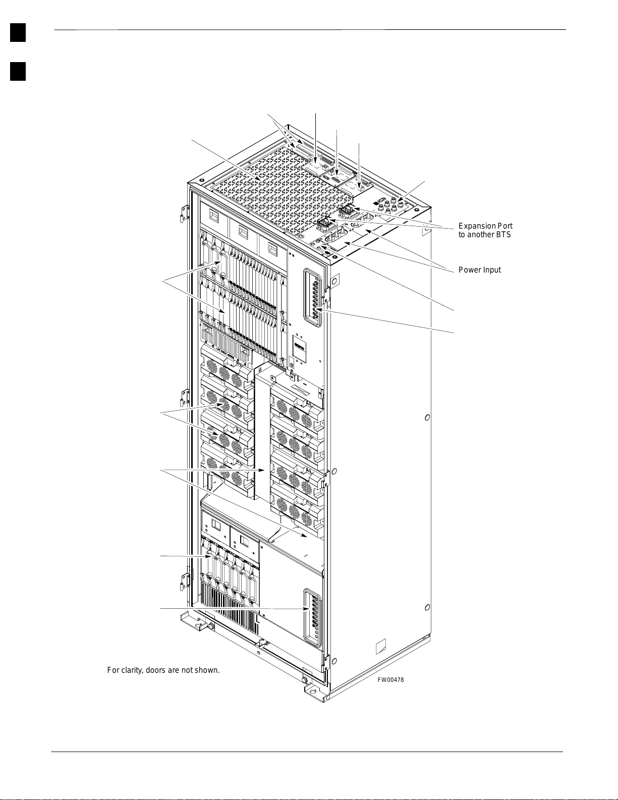
Figure 1-5: –48 V SC 4812T BTS Expansion Frame
Alarms
Span I/O A
C–CCP Cage
LPA Cage
Exhaust Region
Site I/O
Span I/O B
TX Out (1 – 6)
Expansion Port
to another BTS
Power Input
Connection
LAN
Breakers
Combiner
Section
Power
Conversion
Shelf
Breakers
For clarity, doors are not shown.
FW00478
1-18
SC 4812T CDMA BTS Optimization/ATP
May 2000
Page 43

Frame Module Location & Identification
1
Figure 1-6: +27 V SC 4812T Starter Frame I/O Plate
ALARM
ALARM B
ALARM A
RGD
CONNECTORS
SPAN I/O A
SITE I/OSPAN I/O
REAR
SPAN I/O ASPAN I/O B
SITE I/O
RECEIVE ANTENNA
CONNECTORS
SPAN I/O
SPAN I/O B
LOW FREQUENCY
RECEIVER / HSO
1A
1B
LFR/
HSO
2A
2B
RX
3A
3B
4A
4B
LIVE TERMINALSLIVE TERMINALS +27 VDC
5A
5B
6B
6A
GND
4
1
TRANSMIT
ANTENNA
5
2
TX OUT
6
3
CONNECTORS
POWER INPUT
FRONT
CAUTION
EXP I/O
GPS
GPS IN LAN CONNECTIONS
RF EXPANSION PORT
LAN
OUT
AB
LAN
IN
AB
FW00215
(TO ANOTHER BTS)
May 2000
SC 4812T CDMA BTS Optimization/ATP
1-19
Page 44
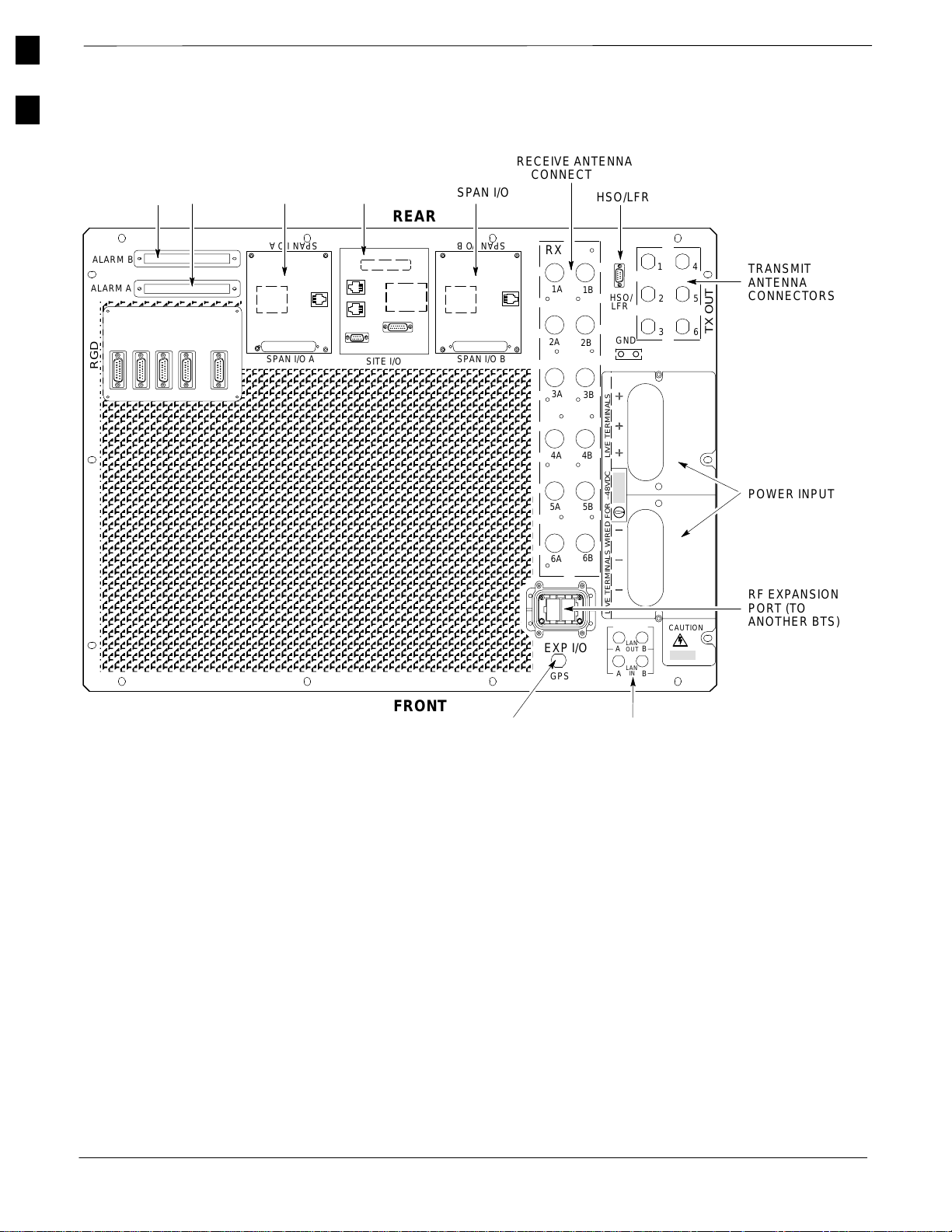
1
Frame Module Location & Identification – continued
Figure 1-7: –48 V SC 4812T Starter Frame I/O Plate
RECEIVE ANTENNA
CONNECTORS
HSO/LFR
RX
1A
1B
2A
2B
3A
3B
4A
4B
4
1
HSO/
LFR
GND
3
2
LIVE TERMINALSLIVE TERMINALS WIRED FOR –48VDC
1
5
2
TX OUT
6
3
TRANSMIT
ANTENNA
CONNECTORS
ALARM B
ALARM A
RGD
ALARM
CONNECTORS
SPAN I/O
SPAN I/O A
SITE I/O
SPAN I/O
REAR
SITE I/O
SITE I/O
SPAN I/O B
SPAN I/O ASPAN I/O B
FRONT
GPS IN
5A
6A
A
EXP I/O
GPS
5B
3
6B
2
RX
1
B
LAN
OUT
AB
LAN
IN
AB
LAN
CONNECTIONS
CAUTION
FW00479
POWER INPUT
RF EXPANSION
PORT (TO
ANOTHER BTS)
1-20
SC 4812T CDMA BTS Optimization/ATP
May 2000
Page 45

Frame Module Location & Identification – continued
Figure 1-8: +27 V SC 4812T Expansion Frame I/O Plate
SITE I/O LFR/HSO
REAR
SITE I/O
SPAN I/O B
AB
EXP IN
ALARM B
ALARM A
RGD
SPAN I/O SPAN I/O
SPAN I/O ASPAN I/O B
SPAN I/O A
4
1
LFR/
2
3
GND
5
6
HSO
LIVE TERMINALSLIVE TERMINALS +27 VDC
1
TRANSMIT
ANTENNA
CONNECTORS
TX OUT
EXP IN
HOUSING
FRONT
AB
EXP OUT
LAN
OUT
AB
GPS
LAN
IN
AB
CAUTION
FW00082
POWER
INPUT
EXP OUT
HOUSING (ADDED
ONLY WHEN
USING SECOND
EXPANSION
FRAME)
LAN
May 2000
SC 4812T CDMA BTS Optimization/ATP
1-21
Page 46

1
Frame Module Location & Identification – continued
Figure 1-9: –48 V SC 4812T Expansion Frame I/O Plate
RF FILTER PORTS NOT USED
IN EXPANSION FRAME
ALARM B
ALARM A
RGD
SPAN I/O SPAN I/O
SITE I/O
REAR
SITE I/O
SITE I/O
SPAN I/O B
SPAN I/O ASPAN I/O B
SPAN I/O A
FRONT
HSO/LFR
1
HSO/
2
LFR
3
GND
AB
EXP IN
A
EXP OUT
B
GPS
3
2
LIVE TERMINALS
1
3
2
1
LIVE TERMINALS WIRED FOR –48 VDC
LAN
OUT
AB
LAN
IN
AB
4
5
6
CAUTION
FW00480
TRANSMIT
ANTENNA
CONNECTORS
TX OUT
EXP IN
HOUSING
POWER
INPUT
EXP OUT
HOUSING (ADDED
ONLY WHEN
USING SECOND
EXPANSION
FRAME)
LAN
1-22
SC 4812T CDMA BTS Optimization/ATP
May 2000
Page 47

Frame Module Location & Identification – continued
Figure 1-10: SC 4812T C–CCP Shelf
1
PS–1
19 mm Filler Panel
CSM–1
HSO/LFR
PS–2
CSM–2
PS–3
CCD–2 CCD–1
AMR–1
GLI2–1GLI2–2
AMR–2
38 mm Filler Panel
MCC24–2
MCC24–1
MCC24–8
MCC24–7
MCC24–4
MCC24–3
MCC24–9
MCC24–10
MCC24–6
MCC24–5
MCC24–11
MCC24–12
BBX2–1
BBX2–2
BBX2–7
BBX2–8
BBX2–3
BBX2–4
BBX2–9
BBX2–10
BBX2–5
BBX2–6
BBX2–11
BBX2–12
BBX2–RSwitch
MPC/EMPC–1MPC/EMPC–2
CIO
NOTE: MCCs may be
MCC24s or MCC8Es.
FW00295
May 2000
SC 4812T CDMA BTS Optimization/ATP
1-23
Page 48

1
Frame Module Location & Identification – continued
Figure 1-11: +27 V SC 4812T LPA Configuration – 4 Carrier with 2:1 Combiners
FAN
MODULE
(TYPICAL)
FILTERS /
COMBINERS
(2 TO 1 COMBINER
SHOWN)
LPA1A
LPA1B
LPA1C
LPA1D
123
456
LPA3A
LPA3B
LPA3C
LPA2A
LPA2B
LPA2C
LPA2D
LPA4A
LPA4B
LPA4C
FW00296
4–CARRIER CONFIGURATION
CARRIER
1
123
456
3
CARRIER
2
4
LPA3D
LPA4D
Note
No adjacent carriers may exist within the same TX filter
combiner. “Adjacent” is defined as fc1 and fc2 being
1.25 MHz apart (center–to–center). “Non–adjacent” is
defined as fc1 and fc2 being >2.50 MHz apart
(center–to–center).
1-24
SC 4812T CDMA BTS Optimization/ATP
May 2000
Page 49

Frame Module Location & Identification – continued
Figure 1-12: –48 V SC 4812T LPA Configuration – 4 Carrier, 3–Sector with 2:1 Combiners
1
FAN
MODULE
(TYPICAL)
FILTERS /
COMBINERS
(2 TO 1 COMBINER
SHOWN)
LPA1A
LPA1B
LPA1C
LPA1D
LPA3A
LPA3B
LPA3C
LPA3D
3
LPA2A
LPA2B
LPA2C
LPA2D
LPA4A
LPA4B
LPA4C
LPA4D
6
FW00481
–48 Volt
SC 4812T
4
1
5
2
4–CARRIER CONFIGURATION
CARRIER CARRIER
4
1
3 4
1
5
2
Sector Configuration
Note
No adjacent carriers may exist within the same TX filter
combiner. “Adjacent” is defined as fc1 and fc2 being
2
1.25 MHz apart (center–to–center). “Non–adjacent” is
defined as fc1 and fc2 being >2.50 MHz apart
(center–to–center).
3
6
There are a number of ways to configure the BTS frame. Table 1-1
outlines the basic requirements. When carrier capacity is greater than
two, a 2:1 or 4:1 cavity combiner must be used. For one or two carriers,
bandpass filters or cavity combiners may be used, depending on
sectorization and channel sequencing.
May 2000
SC 4812T CDMA BTS Optimization/ATP
1-25
Page 50

1
Frame Module Location & Identification – continued
Table 1-1: BTS Sector Configuration
Number
of carriers
1 3 or 6 N/A Bandpass Filter, Cavity Combiner
2 6 Non–adjacent Cavity Combiner (2:1 Only)
2 6 Adjacent Not supported in single frame
2 3 Non–adjacent Cavity Combiner (2:1 or 4:1)
2 3 Adjacent Bandpass Filter
3,4 3 Non–adjacent Cavity Combiner (2:1 or 4:1)
3,4 3 Adjacent Cavity Combiner (2:1 Only)
Number
of sectors
Channel
spacing
Filter requirements
(2:1 or 4:1)
1-26
SC 4812T CDMA BTS Optimization/ATP
May 2000
Page 51

Frame Module Location & Identification – continued
7
Table 1-2: Sector Configurations
Config Ref. No. Description
3–Sector/2–ADJACENT Carriers – The configuration below maps TX with optional 2:1 cavity
combiners for 3 sectors/2 carriers for adjacent channels. Note that 2:1 cavity combiners are used (6
total).
1
2
3
4
5
6
TX1 TX2 TX3 TX4 TX5 TX6 Carrier#
BBX2–1 BBX2–2 BBX2–3 N/A N/A N/A 1
N/A N/A N/A BBX2–4 BBX2–5 BBX2–6 2
6–Sector/2–NON–ADJACENT Carriers – The configuration below maps TX with 2:1 cavity
combiners for 6 sectors/2 carriers for non–adjacent channels.
TX1 TX2 TX3 TX4 TX5 TX6 Carrier#
BBX2–1 BBX2–2 BBX2–3 BBX2–4 BBX2–5 BBX2–6 1
BBX2–7 BBX2–8 BBX2–9 BBX2–10 BBX2–11 BBX2–12 2
3–Sector/2–NON–ADJACENT Carriers – The configuration below maps TX with 2:1 cavity
combiners for 3 sectors/2 carriers for non–adjacent channels.
TX1 TX2 TX3 TX4 TX5 TX6 Carrier#
BBX2–1 BBX2–2 BBX2–3 N/A N/A N/A 1
BBX2–7 BBX2–8 BBX2–9 N/A N/A N/A 2
3–Sector/4–ADJACENT Carriers – The configuration below maps TX with 2:1 cavity combiners
for 3 sector/4 carriers for adjacent channels.
TX1 TX2 TX3 TX4 TX5 TX6 Carrier#
BBX2–1 BBX2–2 BBX2–3 N/A N/A N/A 1
BBX2–7 BBX2–8 BBX2–9 N/A N/A N/A 2
N/A N/A N/A BBX2–4 BBX2–5 BBX2–6 3
N/A N/A N/A BBX2–10 BBX2–11 BBX2–12 4
3–Sector / 2–ADJACENT Carriers – The configuration below maps TX with bandpass filters for
3 sectors/2 carriers for adjacent channels.
TX1 TX2 TX3 TX4 TX5 TX6 Carrier#
BBX2–1 BBX2–2 BBX2–3 N/A N/A N/A 1
N/A N/A N/A BBX2–7 BBX2–8 BBX2–9 2
3–Sector/3 or 4–NON–ADJACENT Carriers – The configuration below maps TX with 4:1
cavity combiners for 3 sectors/3 or 4 carriers for non–adjacent channels.
TX1 TX2 TX3 TX4 TX5 TX6 Carrier#
BBX2–1 BBX2–2 BBX2–3 N/A N/A N/A 1
BBX2–7 BBX2–8 BBX2–9 N/A N/A N/A 2
BBX2–4 BBX2–5 BBX2–6 N/A N/A N/A 3
BBX2–10 BBX2–11 BBX2–12 N/A N/A N/A 4
6–Sector/1–Carrier – The configuration below maps TX with either bandpass filters or 2:1 cavity
combiners for 6 sector/1 carrier.
TX1 TX2 TX3 TX4 TX5 TX6 Carrier#
BBX2–1 BBX2–2 BBX2–3 BBX2–4 BBX2–5 BBX2–6 1
1
May 2000
SC 4812T CDMA BTS Optimization/ATP
1-27
Page 52

1
Frame Module Location & Identification – continued
Figure 1-13: +27 V SC4812T LPA Configuration with Combiners/Filters
Note: See Table 1-2 Configuration
Reference Numbers 1, 2, 3, 4.
Sector
Numbering
3 Sector
(6 Sector)
C1, S1–3
(C1, S1–3)
C3, S1–3
(C1, S4–6)
LPA 1B
LPA 1D
LPA 3B
LPA 3D
2 to 1 Combiner
3 Sector or 6 Sector
LPA 1A
LPA 2B
LPA 1C
LPA 2D
123
456
LPA 3A
LPA 4B
LPA 3C
LPA 4D
LPA 2A
LPA 2C
LPA 4A
LPA 4C
Sector
Numbering
3 Sector
(6 Sector)
C2, S1–3
(C2, S1–3)
C4, S1–3
(C2, S4–6)
Note: See Table 1-2 Configuration
Reference Number 6.
Sector
Numbering
C1, S1–3 C2, S1–3
C3, S1–3 C4, S1–3
LPA 1B
LPA 1D
LPA 3B
LPA 3D
4 to 1 Combiner
3 Sector
LPA 1A
LPA 1C
123
LPA 3A
LPA 3C
LPA 2A
LPA 2B
LPA 2C
LPA 2D
LPA 4A
LPA 4B
LPA 4C
LPA 4D
Numbering
Sector
Note: See Table 1-2 Configuration
Reference Number 5.
Sector
Numbering
3 Sector
C1, S1–3 C2, S1–3
Dual Bandpass Filter
3 Sector Only
2 Carrier Maximum 1 Carrier Only
LPA 1A
LPA 1B
LPA 1C
LPA 1D LPA 2D
123
456
LPA 2B
LPA 2A
LPA 2C
Sector
Numbering
3 Sector
Note: See Table 1-2 Configuration
Reference Number 7.
Sector
Numbering
6 Sector
C1, S1–3
C1, S4–6
Dual Bandpass Filter
LPA 1A
LPA 1B
LPA 1C
LPA 1D
123
456
LPA 3A
LPA 3B
LPA 3C
LPA 3D
6 Sector
FW00297
1-28
SC 4812T CDMA BTS Optimization/ATP
May 2000
Page 53

Frame Module Location & Identification – continued
Figure 1-14: –48 V SC4812T LPA Configuration with Combiners/Filters
1
Note: See Table 1-2 Configuration
Reference Numbers 1, 2, 3, 4.
Sector
Numbering
3 Sector
(6 Sector)
C1, S1–3
(C1, S1–3)
C3, S1–3
(C1, S4–6)
2 to 1 Combiner
3 Sector or 6 Sector
LPA 1A
LPA 1B
LPA 1C
LPA 1D
LPA 3A
LPA 3B
LPA 3C
LPA 3D
4
LPA 2B
1
LPA 2D
5
LPA 4B
2
LPA 4D
Note: See Table 1-2 Configuration
Reference Number 5.
Sector
Numbering
3 Sector
(6 Sector)
LPA 2A
C2, S1–3
LPA 2C
LPA 4A
LPA 4C
36
(C2, S1–3)
C4, S1–3
(C2, S4–6)
Note: See Table 1-2 Configuration
Reference Number 6.
Sector
Numbering
3 Sector
C1, S1–3 C2, S1–3
C3, S1–3 C4, S1–3
4 to 1 Combiner
LPA 1A
LPA 1B
LPA 1C
LPA 1D
LPA 3A
LPA 3B
LPA 3C
LPA 3D
3 Sector
1
2
LPA 2B
LPA 2D
LPA 4B
LPA 4D
LPA 2A
LPA 2C
LPA 4A
LPA 4C
3
Sector
Numbering
3 Sector
Note: See Table 1-2 Configuration
Reference Number 7.
Sector
Numbering
3 Sector
C1, S1–3 C2, S1–3
Dual Bandpass Filter
3 Sector Only
2 Carrier Maximum
LPA 1A
LPA 1B
LPA 1C
LPA 1D LPA 2D
LPA 2B
4
1
5
2
3
6
LPA 2A
LPA 2C
Sector
Numbering
3 Sector
Sector
Numbering
6 Sector
C1, S1–3
C1, S4–6
Dual Bandpass Filter
6 Sector
1 Carrier Only
LPA 1A
LPA 1B
LPA 1C
LPA 1D
LPA 3A
LPA 3B
LPA 3C
LPA 3D
4
1
5
2
3
6
REF FW00482
May 2000
SC 4812T CDMA BTS Optimization/ATP
1-29
Page 54

1
Frame Module Location & Identification – continued
Figure 1-15: –48 V BTS Power Conversion Shelf
REAR
FRONT
AMR
PS–4
FAN
MODULE
PWR/ALM
PS–5
PS–6
REAR
FRONT
PS–7
FAN
MODULE
PWR/ALM
PS–8
PS–9
1A
30
1B
1C
30
1D
2A
30
2B
2C
L
30
2D
P
3A
3B
30
A
3C
30
3D
4A
30
4B
4C
4D
30
FW00501
1-30
SC 4812T CDMA BTS Optimization/ATP
May 2000
Page 55

Frame Module Location & Identification – continued
Figure 1-16: CDMA (COBRA) RFDS Layout
FRONT VIEW
POWER SUPPLY
CASU 1
CASU 2
ON/OFF ROCKER
SWITCH
MMI PORT AND
PWR/ALARM LED
1
FWTIC
(FOR SC 6XX SERIES BTS)
SUA
LEDS
MMI
ESN LABEL
(FOR SC XXXX SERIES BTS)
Cobra RFDS Field Replaceable Unit (FRU)
(shown removed from external housing)
CHASSIS GND
ESN LABEL
ELECTRICAL GND
Cobra RFDS external housing
(Shown With Cover off)
Cobra RFDS RF connector
panel detail
(shown from rear)
FW00138
POWER
CONNECTOR
May 2000
AMR–A
(RS–485 SERIAL)
AMR–B
(RS–485 SERIAL)
SC 4812T CDMA BTS Optimization/ATP
1-31
Page 56

1
Frame Module Location & Identification – continued
Notes
1-32
SC 4812T CDMA BTS Optimization/ATP
May 2000
Page 57

Chapter 2: Preliminary Operations
Table of Contents
Preliminary Operations: Overview 2-1. . . . . . . . . . . . . . . . . . . . . . . . . . . . . . . . . . .
Introduction 2-1. . . . . . . . . . . . . . . . . . . . . . . . . . . . . . . . . . . . . . . . . . . . . .
Cell Site Types 2-1. . . . . . . . . . . . . . . . . . . . . . . . . . . . . . . . . . . . . . . . . . . .
CDF 2-1. . . . . . . . . . . . . . . . . . . . . . . . . . . . . . . . . . . . . . . . . . . . . . . . . . . .
Site Equipage Verification 2-1. . . . . . . . . . . . . . . . . . . . . . . . . . . . . . . . . . .
Initial Installation of Boards/Modules 2-1. . . . . . . . . . . . . . . . . . . . . . . . . .
Setting Frame C–CCP Shelf Configuration Switch 2-3. . . . . . . . . . . . . . .
Pre–Power–up Tests 2-4. . . . . . . . . . . . . . . . . . . . . . . . . . . . . . . . . . . . . . . . . . . . . .
Objective 2-4. . . . . . . . . . . . . . . . . . . . . . . . . . . . . . . . . . . . . . . . . . . . . . . .
Test Equipment 2-4. . . . . . . . . . . . . . . . . . . . . . . . . . . . . . . . . . . . . . . . . . .
Cabling Inspection 2-4. . . . . . . . . . . . . . . . . . . . . . . . . . . . . . . . . . . . . . . . .
DC Power Pre-test (BTS Frame) 2-5. . . . . . . . . . . . . . . . . . . . . . . . . . . . . .
DC Power Pre-test (RFDS) 2-11. . . . . . . . . . . . . . . . . . . . . . . . . . . . . . . . . .
2
Initial Power–up Tests 2-12. . . . . . . . . . . . . . . . . . . . . . . . . . . . . . . . . . . . . . . . . . . .
Power-up Procedures 2-12. . . . . . . . . . . . . . . . . . . . . . . . . . . . . . . . . . . . . . .
Common Power Supply Verification 2-13. . . . . . . . . . . . . . . . . . . . . . . . . . .
Initial Power-up (RFDS) 2-14. . . . . . . . . . . . . . . . . . . . . . . . . . . . . . . . . . . .
Initial Power-up (BTS) 2-14. . . . . . . . . . . . . . . . . . . . . . . . . . . . . . . . . . . . .
May 2000
SC 4812T CDMA BTS Optimization/ATP
Page 58

Table of Contents – continued
Notes
2
SC 4812T CDMA BTS Optimization/ATP
May 2000
Page 59

Preliminary Operations: Overview
Introduction
Cell Site Types
CDF
This section first verifies proper frame equipage. This includes verifying
module placement, jumper, and dual in–line package (DIP) switch
settings against the site-specific documentation supplied for each BTS
application. Next, pre-power up and initial power-up procedures are
presented.
Sites are configured as Omni with a maximum of 4 carriers, 3–sectored
with a maximum of 4 carriers, and 6–sectored with a maximum of 2
carriers. Each type has unique characteristics and must be optimized
accordingly. For more information on the differences in site types, please
refer to the BTS/Modem Frame Hardware Installation manual.
The Cell-site Data File (CDF) contains site type and equipage data
information and passes it directly to the LMF during optimization. The
number of modem frames, C–CCP shelves, BBX2 boards,
MCC24/MCC8E boards (per cage), and linear power amplifier
assignments are some of the equipage data included in the CDF.
IMPORTANT
*
Be sure that the correct bts–#.cdf and cbsc–#.cdf files are
used for the BTS. These should be the CDF files that are
provided for the BTS by the CBSC. Failure to use the
correct CDF files can cause system errors. Failure to use
the correct CDF files to log into a live (traffic carrying)
site can shut down the site.
2
Site Equipage Verification
Initial Installation of
Boards/Modules
May 2000
Review the site documentation. Match the site engineering equipage data
to the actual boards and modules shipped to the site. Physically inspect
and verify the equipment provided for the BTS or Modem frame and
ancillary equipment frame.
CAUTION
Always wear a conductive, high impedance wrist strap
while handling any circuit card/module to prevent damage
by ESD. After removal, the card/module should be placed
on a conductive surface or back into the anti–static
shipping bag.
Follow the procedure in Table 2-1 to verify the initial installation of
boards/modules.
. . . continued on next page
SC 4812T CDMA BTS Optimization/ATP
2-1
Page 60

Preliminary Operations: Overview – continued
Table 2-1: Initial Installation of Boards/Modules
Step Action
2
1 Refer to the site documentation and install all boards and modules into the appropriate shelves as
required. Verify they are NOT SEATED at this time.
NOTE
On 800 MHz systems, the Switch Card has a configuration switch that must match the site
configuration (see Figure 2-1).
2 As the actual site hardware is installed, record the serial number of each module on a “Serial Number
Checklist” in the site logbook.
Figure 2-1: Switch Card
Switch Card
BTS
MF
Configuration
Switch
1234
ON
3 Sector
6 Sector
SHIELDS
J1
J2
J3
J4
J5
NOTE: CONFIGURA TION SWITCH ON
800 MHZ SWITCH CARD ONLY.
SHOWN FOR 3 SECTOR BTS.
SWITCH 1 CHOOSES BTS OR MF.
SWITCH 4 CHOOSES 3–SECTOR OR
6 SECTOR. SWITCHES 2 & 3 ARE NOT
USED.
FW00379
2-2
SC 4812T CDMA BTS Optimization/ATP
68P64114A36–O
May 2000
Page 61

Preliminary Operations: Overview – continued
Setting Frame C–CCP Shelf
Configuration Switch
The backplane switch settings behind the fan module nearest the breaker
panel should be set as shown in Figure 2-2.
The switch setting must be verified and set before power is applied to the
BTS equipment.
Figure 2-2: Backplane DIP Switch Settings – SC 4812T
ON
OFF
ON
OFF
RIGHT / LEFT
BOTTOM / TOP
MODEM_FRAME_ID_1
EXPANSION
FRAME 1
SETTING
MODEM_FRAME_ID_0
EXPANSION
FRAME 2
SETTING
ON
OFF
REAR
PWR/ALM
FRONT
Power Supply
Power Supply
19 mm Filter Panel
FAN
MODULE
Power Supply
RIGHT / LEFT
BOTTOM / TOP
MODULE
REAR
PWR/ALM
FRONT
GLI2GLI2
MCC24–3
MCC24–2
MCC24–1
AMR / MACH
STARTER
FRAME
SETTING
MODEM_FRAME_ID_1
MODEM_FRAME_ID_0
FAN
BBX2–1
BBX2–2
BBX2–3
BBX2–4
BBX2–5
MCC24–6
MCC24–5
MCC24–4
BBX2–6
FAN MODULE
MPCMPC
BBX2–R
2
REMOVED
RIGHT / LEFT
BOTTOM / TOP
MODEM_FRAME_ID_1
MODEM_FRAME_ID_0
HSO
CSM
CSM
BBX2–7
AMR / MACH
CCD CCD
39 mm Filter Panel
MCC24–9
MCC24–8
MCC24–7
MCC24–11
MCC24–12
MCC24–10
BBX2–8
SC 4812T C–CCP SHELF
BBX2–9
BBX2–10
BBX2–11
CIO
Switch
BBX2–12
FW00151REF
May 2000
SC 4812T CDMA BTS Optimization/ATP
2-3
Page 62

Pre–Power–up Tests
Objective
2
Test Equipment
This procedure checks for any electrical short circuits and verifies the
operation and tolerances of the cellsite and BTS power supply units prior
to applying power for the first time.
The following test equipment is required to complete the pre–power–up
tests:
Digital Multimeter (DMM)
CAUTION
Always wear a conductive, high impedance wrist strap
while handling the any circuit card/module to prevent
damage by ESD.
Cabling Inspection
Using the site-specific documentation generated by Motorola Systems
Engineering, verify that the following cable systems are properly
connected:
Receive RF cabling – up to 12 RX cables
Transmit RF cabling – up to six TX cables
GPS
LFR
IMPORTANT
*
For positive power applications (+27 V):
The positive power cable is red.
The negative power cable (ground) is black.
For negative power applications (–48 V):
The negative power cable is red or blue.
The positive power cable (ground) is black.
In all cases, the black power cable is at ground potential.
2-4
SC 4812T CDMA BTS Optimization/ATP
May 2000
Page 63

Pre–Power–up Tests – continued
IMPORTANT
! CAUTION
DC Power Pre-test (BTS Frame)
Before applying any power to the BTS frame, follow the procedure in
Table 2-2 while referring to Figure 2-3 and Figure 2-4 for +27 V
systems or to Figure 2-5 and Figure 2-6 for –48 V systems to verify
there are no shorts in the BTS frame DC distribution system.
Table 2-2: DC Power Pre–test (BTS Frame)
Step Action
1 Physically verify that all DC power sources supplying power to the frame are OFF or disabled.
2 On each frame:
Unseat all circuit boards (except CCD and CIO cards) in the C–CCP shelf and LPA shelves, but
leave them in their associated slots.
Set C–CCP shelf breakers to the OFF position by pulling out power distribution breakers (labeled
C–CCP 1, 2, 3 on the +27 V BTS C–CCP power distribution panel and labeled POWER
1,4,5,2,6,7,3,8,9 on the –48 V C–CCP power distribution panel).
Set LPA breakers to the OFF position by pulling out the LPA breakers (8 breakers, labeled 1A–1B
through 4C–4D – located on the C–CCP power distribution panel in the +27 V BTS or on the power
conversion shelf power distribution panel in the –48 V BTS).
2
3 Verify that the resistance from the power (+ or –) feed terminals with respect to the ground terminal on
the top of the frame measures >
500 Ω (see Figure 2-3).
If reading is < 500 Ω, a short may exist somewhere in the DC distribution path supplied by the
breaker. Isolate the problem before proceeding. A reading > 3 M
missing) bleeder resistor (installed across the filter capacitors behind the breaker panel).
4 Set the C–CCP (POWER) breakers to the ON position by pushing them IN one at a time. Repeat
Step 3 after turning on each breaker.
Ω could indicate an open (or
* IMPORTANT
If the ohmmeter stays at 0 Ω after inserting any board/module, a short probably exists in that
board/module. Replace the suspect board/module and repeat the test. If test still fails, isolate the
problem before proceeding.
5 Insert and lock the DC/DC converter modules for the C–CCP shelf and into their associated slots one
at a time. Repeat Step 3 after inserting each module.
A typical response is that the ohmmeter steadily climbs in resistance as capacitors charge, finally
indicating approximately 500
Verify the correct power/converter modules by observing the locking/retracting tabs appear as follows:
–
–
STPN4009
(in +27 V BTS C–CCP shelf)
PWR CONV CDMA RCVR
STPN4045A
(in –48 V BTS C–CCP shelf)
PWR CONV CDMA RCVR
Ω.
May 2000
6 Insert and lock all remaining circuit boards and modules into their associated slots in the C–CCP shelf.
Repeat Step 3 after inserting and locking each board or module.
A typical response is that the ohmmeter steadily climbs in resistance as capacitors charge, stopping
at approximately 500
Ω..
. . . continued on next page
SC 4812T CDMA BTS Optimization/ATP
2-5
Page 64

Pre–Power–up Tests – continued
indicating approximately 500
Table 2-2: DC Power Pre–test (BTS Frame)
Step Action
2
7 Set the LPA breakers ON by pushing them IN one at a time. Repeat Step 3 after turning on each
breaker.
A typical response is that the ohmmeter will steadily climb in resistance as capacitors charge,
stopping at approximately 500
8 In the –48 V BTS, insert and lock the DC/DC LPA converter modules into their associated slots one at
a time. Repeat Step 3 after inserting each module.
Ω..
A typical response is that the ohmmeter steadily climbs in resistance as capacitors charge, finally
Ω.
! CAUTION
Verify the correct power/converter modules by observing the locking/retracting tabs appear as follows:
STPN4044A
–
(in –48 V BTS power conversion shelf)
PWR CONV LPA
9 Seat all LPA and associated LPA fan modules into their associated slots in the shelves one at a time.
Repeat Step 3 after seating each LPA and associated LPA fan module.
A typical response is that the ohmmeter will steadily climb in resistance as capacitors charge,
stopping at approximately 500
Ω..
2-6
SC 4812T CDMA BTS Optimization/ATP
May 2000
Page 65

Pre–Power–up Tests – continued
Figure 2-3: +27 V BTS DC Distribution Pre-test
LPA
BREAKERS
C–CCP
BREAKERS
TOP OF FRAME
LIVE TERMINALSLIVE TERMINALS +27 VDC
30
1A
1C
2A
2C
L
P
3A
A
3C
4A
4C
1
1B
30
1D
30
2B
30
2D
30
3B
CAUTION
GND
POWER INPUT
30
3D
30
4B
4D
30
50
HSO
3
6
TX OUT
LFR/
2
5
1
4
FW00298
2
C
C
50
2
C
P
3
50
BREAKER PANEL
Breakering:
Two LPAs on each trunking backplane breakered together
Designed for peak LPA current of 15 amps (30 amp breakers)
Unused TX paths do not need to be terminated
Single feed for C–CCP
Dual feed for LPA
. . . continued on next page
May 2000
SC 4812T CDMA BTS Optimization/ATP
2-7
Page 66

Pre–Power–up Tests – continued
Figure 2-4: +27 V SC 4812T BTS Starter Frame
RGD (Needed for
Expansion only)
2
Exhaust Region
C–CCP Cage
Span I/O A
Site I/O
Span I/O B
RX In (1A – 6A
and 1B – 6B)
TX Out (1 – 6)
Power Input
Connection
Expansion I/O
Housing
LPA Cage
Combiner
Section
Breakers
Front Cosmetic
Panel
2-8
For clarity, doors are not shown.
SC 4812T CDMA BTS Optimization/ATP
FW00214
May 2000
Page 67

Pre–Power–up Tests – continued
Figure 2-5: –48 V BTS DC Distribution Pre-test
O
W
R
CAUTION
TOP OF FRAME
LIVE TERMINALSLIVE TERMINALS WIRED FOR –48 VDC
2
2
1
3
1
3
GND
HSO/
LFR
1
2
3
4
5
6
2
TX OUT
1
30
4
40
5
40
P
2
30
6
40
E
7
40
30
3
8
40
9
40
POWER INPUT
1A
30
1B
1C
30
1D
2A
30
2B
2C
L
P
A
3A
3C
4A
30
2D
30
3B
30
3D
30
4B
LPA
BREAKER
C–CCP BREAKER
Breakering:
Two LPAs on each trunking backplane breakered together
Designed for peak LPA current of 15 amps (30 amp breakers)
Unused TX paths do not need to be terminated
Single feed for C–CCP
Dual feed for LPA
4C
4D
30
FW00483
May 2000
SC 4812T CDMA BTS Optimization/ATP
2-9
Page 68

Pre–Power–up Tests – continued
Figure 2-6: –48 V SC 4812T BTS Starter Frame
Alarms
RGD (Needed for
2
Exhaust Region
C–CCP Cage
Expansion only)
Span I/O A
Site I/O
Span I/O B
RX In (1A – 6A
and 1B – 6B)
TX Out (1 – 6)
Power Input
Connection
Expansion I/O
Housing
LPA Cage
Combiner
Section
Power
Conversion
Shelf
Breakers
Front Cosmetic
Panel
2-10
For clarity, doors are not shown.
FW00477
SC 4812T CDMA BTS Optimization/ATP
Breakers
May 2000
Page 69

Pre–Power–up Tests – continued
DC Power Pre-test (RFDS)
Before applying power to the RFDS, follow the steps in Table 2-3, while
referring to Figure 2-7, to verify there are no shorts in the RFDS DC
distribution system, backplanes, or modules/boards. As of the date of
this publication, the RFDS is not used with the –48 V BTS.
2
IMPORTANT
*
Visual inspection of card placement and equipage for each
frame vs. site documentation must be completed, as
covered in Table 2-1, on page 2-2, before proceeding with
this test.
Table 2-3: DC Power Pre-test (RFDS)
Step Action
1 Physically verify that all DC/DC converters supplying the RFDS are OFF or disabled.
2 Set the input power rocker switch P1 to the OFF position (see Figure 2-7).
3 Verify the initial resistance from the power (+ or –) feed terminal with respect to ground terminal
measures >
5 kΩ , then slowly begins to increase.
If the initial reading is < 5 kΩ and remains constant, a short exists somewhere in the DC
distribution path supplied by the breaker. Isolate the problem before proceeding.
4 Set the input power rocker switch P1 to the ON position.
Repeat Step 3.
Figure 2-7: DC Distribution Pre-test (COBRA RFDS Detail)
INPUT POWER
SWITCH (P1)
May 2000
FRONT OF COBRA RFDS
(cut away view shown for clarity)
NOTE:
Set the input power switch ON while measuring the
resistance from the DC power – with respect to the
power + terminal on the rear of the COBRA RFDS.
SC 4812T CDMA BTS Optimization/ATP
RFDS REAR
INTERCONNECT PANEL
“–” CONNECTOR
CONNECTOR (MADE
UP OF A HOUSING
AND TWO PINS)
“+” CONNECTOR
PIN
PIN
FW00139
2-11
Page 70

Initial Power–up Tests
Power-up Procedures
2
WARNING
Potentially lethal voltage and current levels are routed to
the BTS equipment. This test must be performed with a
second person present, acting in a safety role. Remove all
rings, jewelry, and wrist watches prior to beginning this
test.
DC Input Power
In the tests to follow, power will first be verified at the input to each
BTS frame. After power is verified, cards and modules within the frame
itself will be powered up and verified one at a time.
Before applying any power, verify the correct power feed and return
cables are connected between the power supply breakers and the power
connectors at the top of each BTS frame. Verify correct cable position
referring to Figure 2-3 on page 2-7 for +27 V systems and Figure 2-5 on
page 2-9 for –48 V systems.
CAUTION
Always wear a conductive, high impedance wrist strap
while handling any circuit card/module to prevent damage
by ESD. Extreme care should be taken during the removal
and installation of any card/module. After removal, the
card/module should be placed on a conductive surface or
back into the anti–static bag in which it was shipped.
IMPORTANT
*
For positive power applications (+27 V):
The positive power cable is red.
The negative power cable (ground) is black.
For negative power applications (–48 V):
The negative power cable is red or blue.
The positive power cable (ground) is black.
In all cases, the black power cable is at ground potential.
Motorola recommends that the DC input power cable used to connect the
frame to the main DC power source conforms to the guidelines outlined
in Table 2-4.
. . . continued on next page
2-12
SC 4812T CDMA BTS Optimization/ATP
May 2000
Page 71

Initial Power–up Tests – continued
30.38 m (100 ft) 107 mm2 (AWG #4/0)
54.864 m (180 ft) 185 mm2 (350 kcmil)
Greater that 54.864 m (180 ft) Not recommended
Table 2-4: DC Input Power Cable Guidelines
Maximum Cable Length Wire Size
2
IMPORTANT
*
Common Power Supply
Verification
The procedure in Table 2-5 must be performed on any BTS frame
connected to a common power supply at the site after the common power
supply has been installed and verified per the power supply OEM
suggested procedures.
Perform the following steps to verify the power input is within
specification before powering up the individual cards/modules with the
frames themselves.
Table 2-5: Common Power Supply Verification
Step Action
1 Physically verify that all DC power sources supplying the frame are OFF or disabled.
2 On the RFDS (for +27 V systems only), set the input power switch P1 to the OFF position (see
Figure 2-7).
If Anderson SB350 style power connectors are used, make
sure the connector adapters are securely attached to each of
the BTS power feeds and returns. Also, make sure the
cables have been properly installed into each connector.
3 On each frame:
Unseat all circuit boards (except CCD and CIO cards) in the C–CCP shelf and Linear Power
Amplifier (LPA) shelves, but leave them in their associated slots.
Set breakers to the OFF position by pulling out C–CCP and LPA breakers (see Figure 2-3 on
page 2-7 or Figure 2-5 on page 2-9 for breaker panel layout if required).
– C–CCP shelf breakers are labeled CCCP–1, 2, 3 in the +27 V BTS and labeled POWER
1,4,5,2,6,7,3,8,9 in the –48 V BTS.
– LPA breakers are labeled 1A–1B through 4C–4D.
4 Inspect input cables, verify correct input power polarity via decal on top of frame (+27 Vdc or
–48 Vdc).
5 Apply power to BTS frames, one at a time, by setting the appropriate breaker in the power supply that
supplies the frame to the ON position.
6 After power is applied to each frame, use a digital voltmeter to verify power supply output voltages at
nominal.
May 2000
the top of each BTS frame are within specifications: +27.0 Vdc or –48 Vdc
SC 4812T CDMA BTS Optimization/ATP
2-13
Page 72

Initial Power–up Tests – continued
Initial Power-up (RFDS)
The procedure in Table 2-6 must be performed on the RFDS after input
2
power from the common power supply has been verified. Perform the
following steps to apply initial power to the cards/modules within the
frame itself, verifying that each is operating within specification.
IMPORTANT
*
Visual inspection of card placement and equipage for each
frame vs. site documentation must be completed, as
covered in Table 2-1, on page 2-2, before proceeding with
this test.
Table 2-6: Initial Power-up (RFDS)
Step Action
1 On the RFDS, set the input power rocker switch (P1) to the ON position (see Figure 2-7).
2 Verify power supply output voltages (at the top of BTS frame), using a digital voltmeter, are within
specifications: +27.0 V nominal.
Initial Power-up (BTS)
The procedure must be performed on each frame after input power from
the common power supply has been verified. Follow the steps in
Table 2-7 to apply initial power to the cards/modules within the frame
itself, verifying that each is operating within specification.
Table 2-7: Initial Power–up (BTS)
Step Action
1 At the BTS, set the C–CCP (POWER) power distribution breakers (see Figure 2-3 on page 2-7 or
Figure 2-5 on page 2-9) to the ON position by pushing in the breakers.
2 Insert the C–CCP fan modules. Observe that the fan modules come on line.
3
! CAUTION
Verify the correct power/converter modules by observing the locking/retracting tabs appear as follows:
STPN4009
– (in +27 V BTS C–CCP shelf)
PWR CONV CDMA RCVR
STPN 4045A
– (in –48 V BTS C–CCP shelf)
PWR CONV CDMA RCVR
STPN 4044A
– (in –48 V BTS power conversion shelf)
PWR CONV LPA
Insert and lock the converter/power supplies into their associated slots one at a time.
• If no boards have been inserted, all three PWR/ALM LEDs would indicate RED to notify the user
that there is no load on the power supplies.
– If the LED is RED, do not be alarmed. After Step 4 is performed, the LEDs should turn GREEN;
if not, then a faulty converter/power supply module is indicated and should be replaced before
proceeding.
4 Seat and lock all remaining circuit cards and modules in the C–CCP shelf into their associated slots.
. . . continued on next page
2-14
SC 4812T CDMA BTS Optimization/ATP
May 2000
Page 73

Initial Power–up Tests – continued
Table 2-7: Initial Power–up (BTS)
Step Action
5 Seat the first equipped LPA module pair into the assigned slot in the upper LPA shelf including LPA
fan.
In +27 V systems, observe that the LPA internal fan comes on line.
6 Repeat step 5 for all remaining LPAs.
7 Set the LPA breakers to the ON position (per configuration) by pushing them IN one at a time. See
Figure 1-13 on page 1-28 or Figure 1-14 on page 1-29 for configurations and Figure 2-3 on page 2-7
or Figure 2-5 on page 2-9 for LPA breaker panel layout.
On +27 V frames, engage (push) LPA circuit breakers.
Confirm LEDs on LPAs light.
On –48 V frames, engage (push) LPA PS circuit breakers.
Confirm LPA PS fans start.
Confirm LEDs on –48 V power converter boards light.
Confirm LPA fans start.
2
Confirm LEDs on LPAs light.
8 After all cards/modules have been seated and verified, use a digital voltmeter to verify power supply
output voltages at the top of the frame remain within specifications: +27.0 Vdc or –48 Vdc
9 Repeat Steps 1 through 8 for additional co–located frames (if equipped).
nominal.
May 2000
SC 4812T CDMA BTS Optimization/ATP
2-15
Page 74

Initial Power–up Tests – continued
Notes
2
2-16
SC 4812T CDMA BTS Optimization/ATP
May 2000
Page 75

Chapter 3: Optimization/Calibration
Table of Contents
Optimization/Calibration – Introduction 3-1. . . . . . . . . . . . . . . . . . . . . . . . . . . . . .
Introduction 3-1. . . . . . . . . . . . . . . . . . . . . . . . . . . . . . . . . . . . . . . . . . . . . .
Optimization Process 3-1. . . . . . . . . . . . . . . . . . . . . . . . . . . . . . . . . . . . . . .
Cell Site Types 3-2. . . . . . . . . . . . . . . . . . . . . . . . . . . . . . . . . . . . . . . . . . . .
Cell Site Data File (CDF) 3-2. . . . . . . . . . . . . . . . . . . . . . . . . . . . . . . . . . .
BTS System Software Download 3-3. . . . . . . . . . . . . . . . . . . . . . . . . . . . .
Site Equipage Verification 3-3. . . . . . . . . . . . . . . . . . . . . . . . . . . . . . . . . . .
Isolate Span Lines/Connect LMF 3-4. . . . . . . . . . . . . . . . . . . . . . . . . . . . . . . . . . . .
Isolate BTS from T1/E1 Spans 3-4. . . . . . . . . . . . . . . . . . . . . . . . . . . . . . .
LMF to BTS Connection 3-5. . . . . . . . . . . . . . . . . . . . . . . . . . . . . . . . . . . .
Preparing the LMF 3-6. . . . . . . . . . . . . . . . . . . . . . . . . . . . . . . . . . . . . . . . . . . . . . .
Overview 3-6. . . . . . . . . . . . . . . . . . . . . . . . . . . . . . . . . . . . . . . . . . . . . . . .
Graphical User Interface Overview 3-6. . . . . . . . . . . . . . . . . . . . . . . . . . . .
Logical BTS 3-6. . . . . . . . . . . . . . . . . . . . . . . . . . . . . . . . . . . . . . . . . . . . . .
Program and Binaries Update Procedure 3-9. . . . . . . . . . . . . . . . . . . . . . . .
Copy CDF Files from CBSC 3-9. . . . . . . . . . . . . . . . . . . . . . . . . . . . . . . . .
Creating a Named HyperTerminal Connection for MMI Connection 3-11. .
Folder Structure Overview 3-14. . . . . . . . . . . . . . . . . . . . . . . . . . . . . . . . . . .
Pinging the Processors 3-15. . . . . . . . . . . . . . . . . . . . . . . . . . . . . . . . . . . . . .
Logging into a BTS 3-19. . . . . . . . . . . . . . . . . . . . . . . . . . . . . . . . . . . . . . . .
Logging Out 3-20. . . . . . . . . . . . . . . . . . . . . . . . . . . . . . . . . . . . . . . . . . . . . .
3
May 2000
Download the BTS 3-21. . . . . . . . . . . . . . . . . . . . . . . . . . . . . . . . . . . . . . . . . . . . . . .
Download the BTS – Overview 3-21. . . . . . . . . . . . . . . . . . . . . . . . . . . . . . .
Download Code to Devices 3-22. . . . . . . . . . . . . . . . . . . . . . . . . . . . . . . . . .
Download Code and Data to Non–MGLI2 Devices 3-24. . . . . . . . . . . . . . .
Select CSM Clock Source 3-24. . . . . . . . . . . . . . . . . . . . . . . . . . . . . . . . . . .
Enable CSMs 3-25. . . . . . . . . . . . . . . . . . . . . . . . . . . . . . . . . . . . . . . . . . . . .
Enable MCCs 3-27. . . . . . . . . . . . . . . . . . . . . . . . . . . . . . . . . . . . . . . . . . . . .
Enable Redundant GLIs 3-27. . . . . . . . . . . . . . . . . . . . . . . . . . . . . . . . . . . . .
CSM System Time/GPS and LFR/HSO Verification 3-28. . . . . . . . . . . . . . . . . . . . .
CSM & LFR Background 3-28. . . . . . . . . . . . . . . . . . . . . . . . . . . . . . . . . . .
Low Frequency Receiver/
High Stability Oscillator 3-29. . . . . . . . . . . . . . . . . . . . . . . . . . . . . . . . . . . .
Front Panel LEDs 3-29. . . . . . . . . . . . . . . . . . . . . . . . . . . . . . . . . . . . . . . . .
Null Modem Cable 3-30. . . . . . . . . . . . . . . . . . . . . . . . . . . . . . . . . . . . . . . .
CSM Frequency Verification 3-30. . . . . . . . . . . . . . . . . . . . . . . . . . . . . . . . .
SC 4812T CDMA BTS Optimization/ATP
Page 76

Table of Contents – continued
Test Equipment Setup: GPS & LFR/HSO Verification 3-30. . . . . . . . . . . . .
GPS Initialization/Verification 3-32. . . . . . . . . . . . . . . . . . . . . . . . . . . . . . . .
LFR Initialization/Verification 3-35. . . . . . . . . . . . . . . . . . . . . . . . . . . . . . . .
HSO Initialization/Verification 3-38. . . . . . . . . . . . . . . . . . . . . . . . . . . . . . .
Test Equipment Setup 3-39. . . . . . . . . . . . . . . . . . . . . . . . . . . . . . . . . . . . . . . . . . . . .
Connecting Test Equipment to the BTS 3-39. . . . . . . . . . . . . . . . . . . . . . . .
Supported Test Sets 3-39. . . . . . . . . . . . . . . . . . . . . . . . . . . . . . . . . . . . . . . .
Test Equipment Reference Chart 3-40. . . . . . . . . . . . . . . . . . . . . . . . . . . . . .
3
Test Set Calibration 3-49. . . . . . . . . . . . . . . . . . . . . . . . . . . . . . . . . . . . . . . . . . . . . . .
Equipment Warm-up 3-41. . . . . . . . . . . . . . . . . . . . . . . . . . . . . . . . . . . . . . .
Calibrating Cables 3-41. . . . . . . . . . . . . . . . . . . . . . . . . . . . . . . . . . . . . . . . .
Test Set Calibration Background 3-49. . . . . . . . . . . . . . . . . . . . . . . . . . . . . .
Purpose of Test set Calibration 3-49. . . . . . . . . . . . . . . . . . . . . . . . . . . . . . .
Selecting Test Equipment 3-50. . . . . . . . . . . . . . . . . . . . . . . . . . . . . . . . . . .
Manually Selecting Test Equipment in a Serial Connection Tab 3-50. . . . .
Automatically Selecting Test Equipment in a Serial Connection Tab 3-51. .
Calibrating Test Equipment 3-52. . . . . . . . . . . . . . . . . . . . . . . . . . . . . . . . . .
Calibrating Cables 3-52. . . . . . . . . . . . . . . . . . . . . . . . . . . . . . . . . . . . . . . . .
Calibrating Cables with a CDMA Analyzer 3-53. . . . . . . . . . . . . . . . . . . . .
Calibrating TX Cables Using a Signal Generator and
Spectrum Analyzer 3-54. . . . . . . . . . . . . . . . . . . . . . . . . . . . . . . . . . . . . . . .
Calibrating RX Cables Using a Signal Generator and
Spectrum Analyzer 3-55. . . . . . . . . . . . . . . . . . . . . . . . . . . . . . . . . . . . . . . .
Setting Cable Loss Values 3-57. . . . . . . . . . . . . . . . . . . . . . . . . . . . . . . . . . .
Setting TX Coupler Loss Value 3-58. . . . . . . . . . . . . . . . . . . . . . . . . . . . . . .
Bay Level Offset Calibration 3-59. . . . . . . . . . . . . . . . . . . . . . . . . . . . . . . . . . . . . . .
Introduction to Bay Level Offset Calibration 3-59. . . . . . . . . . . . . . . . . . . .
RF Path Bay Level Offset Calibration 3-59. . . . . . . . . . . . . . . . . . . . . . . . . .
When to Calibrate BLOs 3-59. . . . . . . . . . . . . . . . . . . . . . . . . . . . . . . . . . . .
TX Path Calibration 3-60. . . . . . . . . . . . . . . . . . . . . . . . . . . . . . . . . . . . . . . .
BLO Calibration Data File 3-61. . . . . . . . . . . . . . . . . . . . . . . . . . . . . . . . . .
Test Equipment Setup: RF Path Calibration 3-63. . . . . . . . . . . . . . . . . . . . .
TX Path Calibration 3-64. . . . . . . . . . . . . . . . . . . . . . . . . . . . . . . . . . . . . . . .
Download BLO Procedure 3-66. . . . . . . . . . . . . . . . . . . . . . . . . . . . . . . . . . .
Calibration Audit Introduction 3-66. . . . . . . . . . . . . . . . . . . . . . . . . . . . . . .
Transmit (TX) Path Audit 3-67. . . . . . . . . . . . . . . . . . . . . . . . . . . . . . . . . . .
TX Audit Test 3-67. . . . . . . . . . . . . . . . . . . . . . . . . . . . . . . . . . . . . . . . . . . .
All Cal/Audit Test 3-68. . . . . . . . . . . . . . . . . . . . . . . . . . . . . . . . . . . . . . . . .
Create CAL File 3-70. . . . . . . . . . . . . . . . . . . . . . . . . . . . . . . . . . . . . . . . . . .
RFDS Setup and Calibration 3-71. . . . . . . . . . . . . . . . . . . . . . . . . . . . . . . . . . . . . . .
RFDS Description 3-71. . . . . . . . . . . . . . . . . . . . . . . . . . . . . . . . . . . . . . . . .
RFDS Parameter Settings 3-72. . . . . . . . . . . . . . . . . . . . . . . . . . . . . . . . . . .
RFDS TSU NAM Programming 3-74. . . . . . . . . . . . . . . . . . . . . . . . . . . . . .
Explanation of Parameters used when Programming the TSU NAM 3-74. .
Valid NAM Ranges 3-75. . . . . . . . . . . . . . . . . . . . . . . . . . . . . . . . . . . . . . . .
Set Antenna Map Data 3-76. . . . . . . . . . . . . . . . . . . . . . . . . . . . . . . . . . . . . .
Set RFDS Configuration Data 3-77. . . . . . . . . . . . . . . . . . . . . . . . . . . . . . . .
SC 4812T CDMA BTS Optimization/ATP
May 2000
Page 77

Table of Contents – continued
RFDS Calibration 3-78. . . . . . . . . . . . . . . . . . . . . . . . . . . . . . . . . . . . . . . . .
Program TSU NAM 3-79. . . . . . . . . . . . . . . . . . . . . . . . . . . . . . . . . . . . . . . .
BTS Alarms Testing 3-80. . . . . . . . . . . . . . . . . . . . . . . . . . . . . . . . . . . . . . . . . . . . . .
Alarm Test Overview 3-80. . . . . . . . . . . . . . . . . . . . . . . . . . . . . . . . . . . . . . .
Alarm Reporting Display 3-80. . . . . . . . . . . . . . . . . . . . . . . . . . . . . . . . . . . .
Purpose 3-81. . . . . . . . . . . . . . . . . . . . . . . . . . . . . . . . . . . . . . . . . . . . . . . . .
Test Equipment 3-81. . . . . . . . . . . . . . . . . . . . . . . . . . . . . . . . . . . . . . . . . . .
CDI Alarm Input Verification with Alarms Test Box 3-82. . . . . . . . . . . . . .
CDI Alarm Input Verification without Alarms Test Box 3-85. . . . . . . . . . .
Pin and Signal Information for Alarm Connectors 3-86. . . . . . . . . . . . . . . .
3
May 2000
SC 4812T CDMA BTS Optimization/ATP
Page 78

Table of Contents – continued
Notes
3
SC 4812T CDMA BTS Optimization/ATP
May 2000
Page 79

Optimization/Calibration – Introduction
Introduction
This section describes procedures for downloading system operating
software, CSM reference verification/optimization, set up and calibration
of the supported test equipment, transmit/receive path verification, and
using the RFDS.
IMPORTANT
*
Optimization Process
After a BTS is physically installed and the preliminary operations
(power up) have been completed, the LMF is used to calibrate and
optimize the BTS. Motorola recommends that the optimization be
accomplished as follows:
1. Download MGLI2–1 with code and data and then enable MGLI2–1.
2. Use the status function and verify that all of the installed devices of
the following types respond with status information: CSM, BBX2,
GLI2, and MCC (and TSU if RFDS is installed). If a device is
installed and powered up but is not responding and is colored gray in
the BTS display, the device is not listed in the CDF file. The CDF
file will have to be corrected before the device can be accessed by
the LMF.
3. Download code and data to all devices of the following types:
– CSM
– BBX2
– GLI2 (other than MGLI2–1)
– MCC
4. Download the RFDS TSIC (if installed).
5. Verify the operation of the GPS and HSO signals.
6. Enable the following devices (in the order listed):
– Secondary CSM
– Primary CSM
– All MCCs
7. Connect the required test equipment for a full optimization.
8. Select the test equipment.
9. Calibrate the TX and RX test cables if they have not previously been
calibrated using the CDMA LMF that is going to be used for the
optimization/calibration. The cable calibration values can also be
entered manually.
Before using the LMF, use an editor to view the
”CAVEATS” section in the ”readme.txt” file in the c:\wlmf
folder for any applicable information.
3
. . . continued on next page
May 2000
SC 4812T CDMA BTS Optimization/ATP
3-1
Page 80

Optimization/Calibration – Introduction – continued
10. Select all of the BBXs and all of the MCCs and use the full
optimization function. The full optimization function performs TX
calibration, BLO download, TX audit, all TX tests, and all RX tests
for all selected devices.
11. If the TX calibration fails, repeat the full optimization for any failed
paths.
12. If the TX calibration fails again, correct the problem that caused the
failure and repeat the full optimization for the failed path.
3
Cell Site Types
13. If the TX calibration and audit portion of the full optimization passes
for a path but some of the TX or RX tests fail, correct the problem
that caused the failure and run the individual tests as required until
all TX and RX tests have passed for all paths.
Sites are configured as Omni/Omni or Sector/Sector (TX/RX). Each type
has unique characteristics and must be optimized accordingly.
NOTE
Cell Site Data File (CDF)
For more information on the differences in site types,
please refer to the applicable BTS/Modem Frame Hardware
Installation and Functional Hardware Description
manuals.
The CDF contains information that defines the BTS and data used to
download files to the devices. A CDF file must be placed in the
applicable BTS folder before the LMF can be used to log into that BTS.
CDF files are normally obtained from the CBSC using a floppy disk. A
file transfer protocol (ftp) method can be used if the LMF computer has
that capability.
The CDF includes the following information:
Download instructions and protocol
Site specific equipage information
C–CCP shelf allocation plan
– BBX2 equipage (based on cell–site type) including redundancy
– CSM equipage including redundancy
– Multi Channel Card (MCC24 or MCC8E) channel element
allocation plan. This plan indicates how the C–CCP shelf is
configured, and how the paging, synchronization, traffic, and access
channel elements (and associated gain values) are assigned among
the (up to 12) MCC24s or MCC8Es in the shelf.
3-2
CSM equipage including redundancy
SC 4812T CDMA BTS Optimization/ATP
. . . continued on next page
May 2000
Page 81

Optimization/Calibration – Introduction – continued
Effective Rated Power (ERP) table for all TX channels to antennas
respectively. Motorola System Engineering specifies the ERP of a
transmit antenna based on site geography, antenna placement, and
government regulations. Working from this ERP requirement, the
antenna gain, (dependent on the units of measurement specified) and
antenna feed line loss can be combined to determine the required
power at the top of the BTS frame. The corresponding BBX2 output
level required to achieve that power level on any channel/sector can
also be determined.
NOTE
Refer to the CDMA LMF Operator’s Guide, 68P64114A21,
for additional information on the layout of the LMF
directory structure (including CDF file locations and
formats).
BTS System Software
Download
BTS system software must be successfully downloaded to the BTS
processor boards before optimization can be performed. BTS operating
code is loaded from the LMF computer terminal.
3
Site Equipage Verification
IMPORTANT
*
The CDF is normally obtained from the CBSC on a DOS formatted
diskette, or through a file transfer protocol (ftp) if the LMF computer has
ftp capability. Refer to the CDMA LMF Operator’s Guide, or the LMF
Help screen, for the procedure.
If you have not already done so, use an editor to view the CDF, and
review the site documentation. Verify the site engineering equipage data
in the CDF matches the actual site hardware using a CDF conversion
table.
Before using the LMF for optimization/ATP, the correct
bts–#.cdf and cbsc–#.cdf files for the BTS must be
obtained from the CBSC and put in a bts–# folder in the
LMF. Failure to use the correct CDF files can cause wrong
results. Failure to use the correct CDF files to log into a
live (traffic carrying) site can shut down the site.
CAUTION
Always wear a conductive, high impedance wrist strap
while handling any circuit card/module to prevent damage
by ESD. Extreme care should be taken during the removal
and installation of any card/module. After removal, the
card/module should be placed on a conductive surface or
back into the anti–static bag in which it was shipped.
May 2000
SC 4812T CDMA BTS Optimization/ATP
3-3
Page 82

Isolate Span Lines/Connect LMF
Isolate BTS from T1/E1 Spans
IMPORTANT
*
At active sites, the OMC/CBSC must disable the BTS and
place it out of service (OOS). DO NOT remove the 50–pin
TELCO cable connected to the BTS frame site I/O board
J1 connector until the OMC/CBSC has disabled the BTS!
3
Each frame is equipped with one Site I/O and two Span I/O boards. The
Span I/O J1 connector provides connection of 25 pairs of wire. 8 pairs
are used to support up to four 4–wire span lines. 17 pairs are connected
to signal ground.
Before connecting the LMF to the frame LAN, the OMC/CBSC must
disable the BTS and place it OOS to allow the LMF to control the
CDMA BTS. This prevents the CBSC from inadvertently sending
control information to the CDMA BTS during LMF based tests. Refer to
Figure 3-1 and Figure 3-2 as required.
Table 3-1: T1/E1 Span Isolation
Step Action
1 From the OMC/CBSC, disable the BTS and place it OOS. Refer to SC OMC–R/CBSC System
Operator Procedures.
– The T1/E1 span 50–pin TELCO cable connected to the BTS frame SPAN I/O board J1 connector
can be removed from both Span I/O boards, if equipped, to isolate the spans.
* IMPORTANT
Verify that you remove the SPAN cable, not the “MODEM/TELCO” connector.
Figure 3-1: Span I/O Board T1 Span Isolation
SPAN A CONNECTOR
(TELCO) INTERFACE
TO SPAN LINES
RS–232 9–PIN SUB D
CONNECTOR SERIAL
PORT FOR EXTERNAL
DIAL UP MODEM
CONNECTION (IF USED)
TOP OF frame
(Site I/O and Span I/O boards)
50–PIN TELCO
CONNECTORS
REMOVED
FW00299
SPAN B CONNECTOR
(TELCO) INTERFACE
TO SPAN LINES
3-4
SC 4812T CDMA BTS Optimization/ATP
. . . continued on next page
May 2000
Page 83

Isolate Span Lines/Connect LMF – continued
LMF to BTS Connection
The LMF is connected to the LAN A or B connector located on the left
side of the frame’s lower air intake grill, behind the LAN Cable Access
door (see Figure 3-2).
Table 3-2: LMF to BTS Connection
Step Action
1 To gain access to the connectors on the BTS, open the LAN Cable Access door, then pull apart the
Velcro tape covering the BNC “T” connector (see Figure 3-2).
2 Connect the LMF to the LAN A BNC connector via PCMCIA Ethernet Adapter with an unshielded
twisted–pair (UTP) Adapter and 10BaseT/10Base2 converter (powered by an external AC/DC
transformer).
NOTE
– Xircom Model PE3–10B2 or equivalent can also be used to interface the LMF Ethernet
connection to the frame connected to the PC parallel port, powered by an external AC/DC
transformer. In this case, the BNC cable must not exceed 91 cm (3 ft) in length.
* IMPORTANT
– The LAN shield is isolated from chassis ground. The LAN shield (exposed portion of BNC
connector) must not touch the chassis during optimization.
Figure 3-2: LMF Connection Detail
NOTE:
Open LAN CABLE ACCESS
door. Pull apart Velcro tape and
gain access to the LAN A or LAN
B LMF BNC connector.
3
LMF COMPUTER
TERMINAL WITH
MOUSE
May 2000
LMF BNC “T” CONNECTIONS
ON LEFT SIDE OF FRAME
(ETHERNET “A” SHOWN;
ETHERNET “B” COVERED
WITH VELCRO TAPE)
PCMCIA ETHERNET
ADPATER & ETHERNET
UTP ADAPTER
10BASET/10BASE2
CONVERTER
DIRECTLY TO BNC T
CONNECTS
UNIVERSAL TWISTED
PAIR (UTP) CABLE (RJ11
CONNECTORS)
115 VAC POWER
CONNECTION
SC 4812T CDMA BTS Optimization/ATP
FW00140
3-5
Page 84

Preparing the LMF
Overview
Software and files for installation and updating of the LMF are provided
on CD ROM disks. The following installation items must be available:
LMF Program on CD ROM
LMF Binaries on CD ROM
Configuration Data File (CDF) for each supported BTS (on diskette or
3
Graphical User Interface
Overview
available from the CBSC)
CBSC File for each supported BTS (on diskette or available from the
CBSC)
The following section provides information and instructions for
installing and updating the LMF software and files.
The LMF uses a graphical user interface (GUI), which works in the
following way:
Logical BTS
Select the device or devices.
Select the action to apply to the selected device(s).
While action is in progress, a status report window displays the action
taking place and other status information.
The status report window indicates when the the action is complete
and displays other pertinent information.
Clicking the OK button closes the status report window.
The BTS software implements the logical BTS capability, also known as
virtual BTS. Previously, all BTS frames co–located at a single site had to
be identified in the network with separate and distinct BTS ID numbers.
In the Logical BTS feature, all frames located at a single BTS site are
identified with unique Frame ID numbers (Frame ID Numbers 1, 101,
201, 301) under a single (site) BTS ID number. A logical BTS can
consist of up to four SC 4812T frames.When the LMF is connected to
frame 1 of a logical BTS, you can access all devices in all of the frames
that make up the logical BTS. A logical BTS requires a CDF file that
includes equipage information for all of the logical BTS frames and their
devices and a CBSC file that includes channel data for all of the logical
BTS fames.
. . . continued on next page
3-6
SC 4812T CDMA BTS Optimization/ATP
May 2000
Page 85

Preparing the LMF – continued
Logical BTS Numbering
The first frame of a logical BTS has a –1 suffix (e.g., BTS–812–1).
Other frames of the logical BTS are numbered with suffixes, –101, –201,
and –301 (e. g. BTS–812–201). When you log into a BTS, a FRAME
tab is displayed for each frame. If there is only one frame for the BTS,
there is only one tab (e.g., FRAME–282–1) for BTS–282. If a logical
BTS has more than one frame, there is a separate FRAME tab for each
frame (e.g. FRAME–438–1, FRAME–438–101, and FRAME–438–201
for a BTS–438 that has three frames). If an RFDS is included in the
CDF file, an RFDS tab (e.g., RFDS–438–1) is displayed. Figure 3-3
shows frame configurations available under the Logical BTS feature.
This figure also shows the Inter–frame spans between the different
frames at the BTS site.
Actions (e.g., ATP tests) can be initiated for selected devices in one or
more frames of a logical BTS. Refer to the Select devices help screen for
information on how to select devices.
C–CCP Shelf Card/Module Device ID Numbers
3
All cards/modules/boards in the frames at a single site, assigned to a
single BTS number, are also identified with unique Device ID numbers
dependent upon the Frame ID number in which they are located. Refer to
Table 3-3 and Table 3-4 for specific C–CCP Shelf Device ID numbers.
Table 3-3: C–CCP Shelf/Cage Card/Module Device ID Numbers (Top Shelf)
Frame
#
Power
Power
Power
(PS–1)
(PS–2)
1 – – – 1 1 1 2 3 4 5 6 1 2 3 4 5 6 R1 –
101 – – – 101 101 101 102 103 104 105 106 101 102 103 104 105 106 R101 –
201 – – – 201 201 201 202 203 204 205 206 201 202 203 204 205 206 R201 –
301 – – – 301 301 301 302 303 304 305 306 301 302 303 304 305 306 R301 –
(PS–3)
AMR–1GLI2
–1
Card/Module ID Number (Left to Right)
MCC2 BBX2 BBX2–RMPC/
Table 3-4: C–CCP Shelf/Cage Card/Module Device ID Numbers (Bottom Shelf)
Frame
#
HSO/
CSM–1CSM–2CCDACCD
LFR
B
Card/Module ID Number (Left to Right)
AMR–2GLI2–
2
MCC2 BBX2 SW MPC/
EMPC
–1
EMPC
–2
1 – 1 2 – – – 2 2 7 8 9 10 11 12 7 8 9 10 11 12 – –
101 – 101 102 – – – 102 102 107 108 109 110 111 112 107 108 109 110 111 112 – –
201 – 201 202 – – – 202 102 207 208 209 210 211 212 207 208 209 210 211 212 – –
301 – 301 302 – – – 302 102 307 308 309 310 311 312 307 308 309 310 311 312 – –
. . . continued on next page
May 2000
SC 4812T CDMA BTS Optimization/ATP
3-7
Page 86

Preparing the LMF – continued
Figure 3-3: Typical Logical BTS Configurations
Two Frame Configuration Three Frame Configuration
BTSSPAN
1
BTSSPAN 110
AB
BTSSPAN
1
A
BTSSPAN 110 BTSSPAN 211
AA A
B
B
3
Frame
201
Frame
1
BTSSPAN 310
A
Frame
301
Frame
101
Frame
201
Frame
1
BTSSPAN
1
Frame
101
Frame
Four Frame Configuration
BTSSPAN 110
B
1
BTSSPAN 211
Frame
101
BBAA
A
FW00485REF
3-8
SC 4812T CDMA BTS Optimization/ATP
May 2000
Page 87

Preparing the LMF – continued
Program and Binaries Update Procedure
Follow the procedure in Table 3-5 to update the LMF program and
binaries.
NOTE
First Time Installations:
– Install Java Runtime Environment (First)
– Install LMF Software (Second)
– Install BTS Binaries (Third)
– Install/Create BTS Folders (Fourth)
NOTE
If applicable, a separate CD ROM of BTS Binaries may be
available for binary updates.
3
Table 3-5: CD ROM Installation
Step Action
1 Insert the LMF Program CD ROM into the LMF CD ROM drive.
– If the Setup screen is displayed, follow the instructions provided.
– If the Setup screen is not displayed, proceed to step 2.
2 Click on the Start button.
3 Select Run.
4 In the Open box, enter d:\autorun and click on the OK button.
NOTE
If applicable, replace the letter d with the correct CD ROM drive letter.
5 Follow the instructions displayed in the Setup screen.
Copy CDF Files from CBSC
Before the LMF can execute the optimization/ATP procedures for the
BTS, the correct bts-#.cdf and cbsc-#.cdf files must be
obtained from the CBSC and put in a bts-# folder in the LMF
notebook. This requires copying the CBSC CDF files to a DOS
formatted diskette, and using the diskette to install the CDF file in the
LMF.
. . . continued on next page
May 2000
SC 4812T CDMA BTS Optimization/ATP
3-9
Page 88

Preparing the LMF – continued
Follow the procedure in Table 3-6 to obtain the CDF files from the
CBSC and copy the files to a diskette. For any further information, refer
to the CDMA LMF Operator’s Guide (Motorola part number
68P64114A21) or the LMF Help screen..
NOTE
If the LMF has ftp capability, the ftp method can be used to
copy the CDF files from the CBSC.
3
On Sun OS workstations, the unix2dos command can be
used in place of the cp command (e.g., unix2dos
bts–248.cdf bts–248.cdf). This should be done using a
copy of the CBSC CDF file so the original CBSC CDF file
is not changed to DOS format.
IMPORTANT
*
Table 3-6: Copying CBSC CDF Files to the LMF
Step Action
AT THE CBSC:
1 Login to the CBSC workstation.
2 Insert a DOS formatted diskette in the workstation drive.
When copying CDF files, comply with the following to
prevent BTS login problems with the LMF:
– The numbers used in the bts–#.cdf and cbsc–#.cdf
filenames must correspond to the locally assigned numbers
for each BTS and its controlling CBSC.
– The generic cbsc–1.cdf file supplied with the LMF work
with locally numbered BTS CDF files. Using this file does
not provide a valid optimization unless the generic file is
edited to replace default parameters (e.g., channel numbers)
with the operational parameters used locally.
3-10
3 Type eject –q and press the <Enter> key.
4 Type mount and press the <Enter> key.
NOTE
Look for the “floppy/no_name” message on the last line displayed.
If the eject command was previously entered, floppy/no_name will be appended with a number.
Use the explicit floppy/no_name reference displayed when performing step 7.
. . . continued on next page
SC 4812T CDMA BTS Optimization/ATP
May 2000
Page 89

Preparing the LMF – continued
Table 3-6: Copying CBSC CDF Files to the LMF
ActionStep
5 Change to the directory containing the file by typing cd <directoryname> (ex. cd bts–248) and
pressing <Enter>.
6 Type ls <Enter> to display the list of files in the directory.
7 With Solaris versions of Unix, create DOS–formatted versions of the bts–#.cdf and cbsc–#.cdf
files on the diskette by entering the following command:
unix2dos <source filename> /floppy/no_name/<target filename>
(e.g., unix2dos bts–248.cdf /floppy/no_name/bts–248.cdf).
NOTE
Other versions of Unix do not support the unix2dos and dos2unix commands. In these cases,
use the Unix cp (copy) command. The copied files will be difficult to read with a DOS or
Windows text editor because Unix files do not contain line feed characters. Editing copied CDF
files on the LMF computer is, therefore, not recommended.
Using cp, multiple files can be copied in one operation by separating each filename to be copied
with a space and ensuring the destination directory (floppy/no_name) is listed at the end of the
command string following a space (e.g., cp bts–248.cdf cbsc–6.cdf /floppy/na_name)
3
8 Repeat steps 5 through 7 for each bts–# that must be supported by the LMF.
9 When all required files have been copied to the diskette, type eject and press the <Enter> key.
10 Remove the diskette from the CBSC.
AT THE LMF:
11 Start the Windows operating system.
12 Insert the diskette into the LMF.
13 Using Windows Explorer (or equivalent program), create a corresponding bts–# folder in the
wlmf\cdma directory for each bts–#.cdf/cbsc–#.cdf file pair copied from the CBSC.
14 Use Windows Explorer (or equivalent program) to transfer the cbsc–#.cdf and bts–#.cdf files from
the diskette to the corresponding wlmf\cdma\bts–# folders created in step 13.
Creating a Named
HyperTerminal Connection for
MMI Connection
Confirming or changing the configuration data of certain BTS Field
Replaceable Units (FRUs) requires establishing an MMI communication
session between the LMF and the FRU. Using features of the Windows
operating system, the connection properties for an MMI session can be
saved on the LMF computer as a named Windows HyperTerminal
connection. This eliminates the need for setting up connection
parameters each time an MMI session is required to support
optimization.
. . . continued on next page
May 2000
SC 4812T CDMA BTS Optimization/ATP
3-11
Page 90

Preparing the LMF – continued
Once the named connection is saved, a shortcut for it can be created on
the Windows desktop. Double clicking the shortcut icon will start the
connection without the need to negotiate multiple menu levels.
Follow the procedure in Table 3-7 to establish a named HyperTerminal
connection and create a WIndows desktop shortcut for it.
3
Table 3-7: Creating a Named Hyperlink Connection for MMI Connection
Step Action
1 From the Windows Start menu, select:
Programs>Accessories
2 Perform one of the following:
NOTE
There are differences between Windows NT and Windows
98 in the menus and screens for creating a HyperTerminal
connection. In the following procedure, items applicable
to:
– Windows NT will be identified with Win NT
– Windows 98 will be identified with Win 98
For Win NT, select Hyperterminal and then click on HyperTerminal
For Win 98, select Communications, double click the Hyperterminal folder, and then double click
on the Hyperterm.exe icon in the window that opens.
NOTE
If a Location Information Window appears, enter the required information, then click Close.
(This is required the first time, even if a modem is not to be used.)
If a You need to install a modem..... message appears, click NO.
3 When the Connection Description box opens:
– Type a name for the connection being defined (e.g., MMI Session) in the Name: window.
– Highlight any icon preferred for the named connection in the Icon: chooser window, and
– Click OK.
NOTE
For LMF configurations where COM1 is used by another interface such as test equipment and a
physical port is available for COM2, select COM2 to prevent conflicts.
4
From the Connect using: pick list in the Connect To box displayed, select the RS–232 port to be used
for the connection (e.g., COM1 or COM2 – Win NT – or Direct to Com 1 or Direct to Com 2 – Win
98), and click OK.
3-12
SC 4812T CDMA BTS Optimization/ATP
. . . continued on next page
May 2000
Page 91

Preparing the LMF – continued
Table 3-7: Creating a Named Hyperlink Connection for MMI Connection
Step Action
5 In the Port Settings tab of the COM# Properties window displayed, configure the RS–232 port
settings as follows:
Bits per second: 9600
Data bits: 8
Parity: None
Stop bits: 1
Flow control: None
6 Click OK.
7 Save the defined connection by selecting:
File>Save
8 Close the HyperTerminal window by selecting:
File>Exit
9 Click Yes to disconnect when prompted.
10 Perform one of the following:
If the Hyperterminal folder window is still open (Win 98) proceed to step 12
From the Windows Start menu, select Programs > Accessories
11 Perform one of the following:
For Win NT, select Hyperterminal and release any pressed mouse buttons.
For Win 98, select Communications and double click the Hyperterminal folder.
12 Highlight the newly created connection icon by moving the cursor over it (Win NT) or clicking on it
(Win 98).
3
13 Right click and drag the highlighted connection icon to the Windows desktop and release the right
mouse button.
14 From the pop–up menu displayed, select Create Shortcut(s) Here.
15 If desired, reposition the shortcut icon for the new connection by dragging it to another location on the
Windows desktop.
May 2000
SC 4812T CDMA BTS Optimization/ATP
3-13
Page 92

Preparing the LMF – continued
Folder Structure Overview
The LMF uses a wlmf folder that contains all of the essential data for
installing and maintaining the BTS. The list that follows outlines the
folder structure for the LMF. Except for the bts–nnn folders, these
folders are created as part of the the LMF installation. Refer to the
CDMA LMF Operator’s Guide for a complete description of the folder
structure.
3
Figure 3-4: LMF Folder Structure
(C:)
wlmf
folder
cdma
folder
BTS–nnn
required for each BTS where bts–nnn is the
unique BTS number; for example, bts–163)
loads
folders (A separate folder is
folder
version folder (A separate folder is
required for each different version; for
example, a folder name 2.8.1.1.1.5)
code
folder
data
folder
3-14
SC 4812T CDMA BTS Optimization/ATP
May 2000
Page 93

Preparing the LMF – continued
Pinging the Processors
For proper operation, the integrity of the Ethernet LAN A and B links
must be be verified. Figure 3-5 represents a typical BTS Ethernet
configuration. The drawing depicts one (of two identical) links, A and B.
Ping is a program that routes request packets to the LAN network
modules to obtain a response from the specified “targeted” BTS.
Figure 3-5: BTS LAN Interconnect Diagram
OUT
IN
50Ω
B
SIGNAL
GROUND
LMF CONNECTOR
C–CCP
CAGE
AB
A
IN
OUT
BTS
(master)
A
B
CHASSIS
GROUND
SIGNAL
GROUND
50Ω
SIGNAL
GROUND
C–CCP
CAGE
AB
IN
B
A
IN
A
OUT
B
BTS
(expansion)
OUT
FW00141
CHASSIS
GROUND
SIGNAL
GROUND
3
50Ω
May 2000
Follow the procedure in Table 3-8 and refer to Figure 3-6 or Figure 3-7,
as required, to ping each processor (on both LAN A and LAN B) and
verify LAN redundancy is operating correctly.
CAUTION
Always wear a conductive, high impedance wrist strap
while handling any circuit card/module to prevent damage
by ESD.
IMPORTANT
*
The Ethernet LAN A and B cables must be installed on
each frame/enclosure before performing this test. All other
processor board LAN connections are made via the
backplanes.
. . . continued on next page
SC 4812T CDMA BTS Optimization/ATP
3-15
Page 94

Preparing the LMF – continued
Table 3-8: Pinging the Processors
Step Action
1 If you have not already done so, connect the LMF to the BTS (see Table 3-2 on page 3-5).
2 From the Windows desktop, click the Start button and select Run.
3 In the Open box, type ping and the MGLI IP address (for example, ping 128.0.0.2).
NOTE
3
128.0.0.2 is the default IP address for MGLI–1 in field BTS units. 128.0.0.1 is the default IP address
for MGLI–2.
4 Click on the OK button.
5 If the connection is successful, text similar to the following is displayed:
Reply from 128 128.0.0.2: bytes=32 time=3ms TTL=255
If there is no response the following is displayed:
Request timed out
If the MGLI fails to respond, reset and perform the ping process again. If the MGLI still fails to
respond, typical problems are shorted BNC to inter-frame cabling, open cables, crossed A and B link
cables, missing 50–Ohm terminators, or the MGLI itself.
3-16
SC 4812T CDMA BTS Optimization/ATP
May 2000
Page 95

Preparing the LMF – continued
Figure 3-6: +27 V SC 4812T Starter Frame I/O Plate
REAR
ALARM B
ALARM A
RGD
SPAN I/O A
SITE I/O
TOP VIEW
SPAN I/O B
FRONT
1
1A
2A
RX
3A
4A
5A
6A
EXP I/O
GPS
1B
LFR/
HSO
2B
3B
4B
LIVE TERMINALSLIVE TERMINALS +27 VDC
5B
6B
GND
LAN
OUT
AB
LAN
IN
AB
2
3
CAUTION
FW00081
ETHERNET CONNECTORS
WITH 50–OHM TERMINAT ORS
4
5
6
TX OUT
3
May 2000
SC 4812T CDMA BTS Optimization/ATP
3-17
Page 96

Preparing the LMF – continued
Figure 3-7: –48 V SC 4812T Starter Frame I/O Plate
REAR
SITE I/O
SITE I/O
SPAN I/O B
RX
2A
5A
4
1
1A
1B
HSO/
LFR
GND
2B
3A
3B
1
2
4A
4B
LIVE TERMINALSLIVE TERMINALS –48 VDC
3
5B
1
6B
6A
RX
2
5
2
TX OUT
6
3
SPAN I/O ASPAN I/O B
ALARM B
ALARM A
3
RGD
SPAN I/O A
FRONT
3
A
EXP I/O
GPS
B
AB
AB
LAN
OUT
LAN
CAUTION
IN
FW00479
REF
ETHERNET CONNECTORS
WITH 50–OHM TERMINAT ORS
3-18
SC 4812T CDMA BTS Optimization/ATP
May 2000
Page 97
Preparing the LMF – continued
Logging into a BTS
Logging into a BTS establishes a communications link between the BTS
and the CDMA LMF. You may be logged into one or more BTS’s at a
time, but only one LMF may be logged into each BTS.
IMPORTANT
*
Before attempting to log into the BTS, confirm the LMF is properly
connected to the BTS (see Figure 3-2). Follow the procedure in
Table 3-9 to log into a BTS.
Prerequisites
Before attempting to login to a BTS, ensure the following have been
completed:
Be sure that the correct bts–#.cdf and cbsc–#.cdf file is
used for the BTS. These should be the CDF files that are
provided for the BTS by the CBSC. Failure to use the
correct CDF files can result in wrong results. Failure to
use the correct CDF files to log into a live (traffic
carrying) site can shut down the site.
A bts-nnn folder with the correct CDF file and CBSC file exists.
The LMF is correctly installed and prepared, and the LMF computer
was connected to the BTS before starting the Windows operating
system and LMF software. If necessary, restart the computer after
connecting it to the BTS (see Table 3-2 and Figure 3-2).
Table 3-9: BTS Login Procedure
3
Step Action
1 Click on the Login tab (if not displayed).
2 If no base stations can be seen, double click on CDMA (in the Available base Stations pick list).
3 Click on the desired BTS number.
4 Click on the Network Login tab (if not already in the forefront).
5 Enter correct IP address (normally 128.0.0.2) for a field BTS, if not correctly displayed in the IP
Address box.
NOTE
128.0.0.2 is the default IP address for MGLI–1 in field BTS units. 128.0.0.1 is the default IP
address for MGLI–2.
6 Type in the correct IP Port number (normally 9216) if not correctly displayed in the IP Port box.
7 Change the Multi-Channel Preselector (from the Multi-Channel Preselector pick list), normally
MPC, corresponding to your BTS configuration, if required.
8 Click on the Use a Tower Top Amplifier, if applicable.
May 2000
SC 4812T CDMA BTS Optimization/ATP
. . . continued on next page
3-19
Page 98

Preparing the LMF – continued
Table 3-9: BTS Login Procedure
ActionStep
9 Click on Login .
A BTS tab with the BTS is displayed.
NOTE
If you attempt to login to a BTS that is already logged on, all devices will be gray.
3
Logging Out
There may be instances where the BTS initiates a logout due to a system error (i.e., a device
failure).
If the MGLI is OOS_ROM (blue), it must be downloaded with code before other devices can be
seen.
Follow the procedure in Table 3-10 to logout of a BTS.
Prerequisites
The LMF is logged into the BTS.
Table 3-10: Logout Procedure
Step Action
1 Click on the Select menu.
2 Click on Logout from the Select menu list.
A Confirm Logout pop–up message appears.
3 Click on Yes (or press the <Enter> key) to confirm logout and return to the Login tab.
NOTE
The Select menu will only logout of the displayed BTS. You may also logout of all BTS login
sessions and exit the LMF by using the File>Exit menu item.
3-20
SC 4812T CDMA BTS Optimization/ATP
May 2000
Page 99

Download the BTS
Download the BTS – Overview
Before a BTS can operate, each equipped device must contain device
initialization (ROM) code. ROM code is loaded in all devices during
manufacture or factory repair. Device application (RAM) code and data
must be downloaded to each equipped device by the user before the BTS
can be made fully functional for the site where it is installed.
ROM Code
Downloading ROM code to BTS devices from the LMF is NOT routine
maintenance nor a normal part of the optimization process. It is only
done in unusual situations where the resident ROM code in the device
does not match the release level of the site operating software (e.g.,
Release 8.x ROM code and Release 9.x software) AND the CBSC cannot
communicate with the BTS to perform the download. If you must
download ROM code, refer to Appendix H.
Before ROM code can be downloaded from the LMF, the correct ROM
code file for each device to be loaded must exist on the LMF computer.
ROM code must be manually selected for download.
RAM Code
Before RAM code can be downloaded from the CDMA LMF, the correct
RAM code file for each device must exist on the LMF computer. RAM
code can be automatically or manually selected depending on the Device
menu item chosen and where the RAM code file for the device is stored
in the CDMA LMF file structure. The RAM code file is selected
automatically if the file is in the \lmf\cdma\loads\n.n.n.n\code folder
(where n.n.n.n is the version number of the download code). The RAM
code file in the code folder must have the correct hardware bin number.
3
May 2000
RAM code can be downloaded to a device that is in any state. After the
download is started, the device being downloaded changes to OOS-ROM
(blue). When the download is completed successfully, the device
changes to OOS-RAM (yellow). When code is downloaded to an MGLI,
the LMF automatically also downloads data, and then enables the MGLI.
When enabled, the MGLI changes to INS (green).
For non–MGLI devices, data must be downloaded after RAM code is
downloaded. To download data, the device state must be OOS–RAM
(yellow).
SC 4812T CDMA BTS Optimization/ATP
3-21
Page 100

Download the BTS – continued
Download Code to Devices
Code can be downloaded to a device that is in any state. After the
download starts, the device being downloaded changes to
OOS_ROM (blue). If the download is completed successfully, the device
changes to OOS_RAM with code loaded (yellow). Prior to downloading
a device, a code file must exist. The code file is selected automatically if
the code file is in the /lmf/cdma/n.n.n.n/code folder (where n.n.n.n is the
version number of the download code that matches the “NextLoad”
3
parameter in the CDF file). The code file in the code folder must have
the correct hardware bin number. Code can be automatically or manually
selected.
The following are the devices to be downloaded:
Span Configuration
– Master Group Line Interface (MGLI2)
– Slave Group Line Interface (SGLI2)
Clock Synchronization Module (CSM)
Multi Channel Card (MCC24 or MCC8E)
Broadband Transceiver (BBX2)
Test Subscriber Interface Card (TSIC) – if RFDS is installed
IMPORTANT
*
Follow the procedure in Table 3-11 to download the firmware
application code for the MGLI2. The download code action downloads
data and also enables the MGLI2.
Prerequisite
Prior to performing this procedure, ensure a code file exists for each of
the devices to be downloaded.
The MGLI must be successfully downloaded with code and
data, and put INS before downloading any other device.
The download code process for an MGLI automatically
downloads data and enables the MGLI before downloading
other devices. The other devices can be downloaded in any
order.
. . . continued on next page
3-22
SC 4812T CDMA BTS Optimization/ATP
May 2000
 Loading...