

Page 1

Nokia Customer Care
Service Manual
RM-704 (Nokia C2-00)
Mobile Terminal
Part No: (Issue 1)
COMPANY CONFIDENTIAL
Copyright © 2011 Nokia. All rights reserved.
Page 2
Amendment Record Sheet
Amendment No Date Inserted By Comments
Original issue 05/2011 Jeff Zhao
RM-704
Amendment Record Sheet
Page ii COMPANY CONFIDENTIAL Issue 1
Copyright © 2011 Nokia. All rights reserved.
Page 3

RM-704
Copyright
Copyright
Copyright © 2011 Nokia. All rights reserved.
Reproduction, transfer, distribution or storage of part or all of the contents in this document in any form
without the prior written permission of Nokia is prohibited.
Nokia, Nokia Connecting People, and Nokia X and Y are trademarks or registered trademarks of Nokia
Corporation. Other product and company names mentioned herein may be trademarks or tradenames of
their respective owners.
Nokia operates a policy of continuous development. Nokia reserves the right to make changes and
improvements to any of the products described in this document without prior notice.
Under no circumstances shall Nokia be responsible for any loss of data or income or any special, incidental,
consequential or indirect damages howsoever caused.
The contents of this document are provided "as is". Except as required by applicable law, no warranties of
any kind, either express or implied, including, but not limited to, the implied warranties of merchantability
and fitness for a particular purpose, are made in relation to the accuracy, reliability or contents of this
document. Nokia reserves the right to revise this document or withdraw it at any time without prior notice.
The availability of particular products may vary by region.
IMPORTANT
This document is intended for use by qualified service personnel only.
Issue 1 COMPANY CONFIDENTIAL Page iii
Copyright © 2011 Nokia. All rights reserved.
Page 4

RM-704
Warnings and cautions
Warnings and cautions
Warnings
•
IF THE DEVICE CAN BE INSTALLED IN A VEHICLE, CARE MUST BE TAKEN ON INSTALLATION IN VEHICLES FITTED
WITH ELECTRONIC ENGINE MANAGEMENT SYSTEMS AND ANTI-SKID BRAKING SYSTEMS. UNDER CERTAIN FAULT
CONDITIONS, EMITTED RF ENERGY CAN AFFECT THEIR OPERATION. IF NECESSARY, CONSULT THE VEHICLE DEALER/
MANUFACTURER TO DETERMINE THE IMMUNITY OF VEHICLE ELECTRONIC SYSTEMS TO RF ENERGY.
•
THE PRODUCT MUST NOT BE OPERATED IN AREAS LIKELY TO CONTAIN POTENTIALLY EXPLOSIVE ATMOSPHERES,
FOR EXAMPLE, PETROL STATIONS (SERVICE STATIONS), BLASTING AREAS ETC.
•
OPERATION OF ANY RADIO TRANSMITTING EQUIPMENT, INCLUDING CELLULAR TELEPHONES, MAY INTERFERE
WITH THE FUNCTIONALITY OF INADEQUATELY PROTECTED MEDICAL DEVICES. CONSULT A PHYSICIAN OR THE
MANUFACTURER OF THE MEDICAL DEVICE IF YOU HAVE ANY QUESTIONS. OTHER ELECTRONIC EQUIPMENT MAY
ALSO BE SUBJECT TO INTERFERENCE.
•
BEFORE MAKING ANY TEST CONNECTIONS, MAKE SURE YOU HAVE SWITCHED OFF ALL EQUIPMENT.
Cautions
•
Servicing and alignment must be undertaken by qualified personnel only.
•
Ensure all work is carried out at an anti-static workstation and that an anti-static wrist strap is worn.
•
Ensure solder, wire, or foreign matter does not enter the telephone as damage may result.
•
Use only approved components as specified in the parts list.
•
Ensure all components, modules, screws and insulators are correctly re-fitted after servicing and
alignment.
•
Ensure all cables and wires are repositioned correctly.
•
Never test a mobile phone WCDMA transmitter with full Tx power, if there is no possibility to perform the
measurements in a good performance RF-shielded room. Even low power WCDMA transmitters may disturb
nearby WCDMA networks and cause problems to 3G cellular phone communication in a wide area.
•
During testing never activate the GSM or WCDMA transmitter without a proper antenna load, otherwise
GSM or WCDMA PA may be damaged.
Page iv COMPANY CONFIDENTIAL Issue 1
Copyright © 2011 Nokia. All rights reserved.
Page 5

RM-704
For your safety
For your safety
QUALIFIED SERVICE
Only qualified personnel may install or repair phone equipment.
ACCESSORIES AND BATTERIES
Use only approved accessories and batteries. Do not connect incompatible products.
CONNECTING TO OTHER DEVICES
When connecting to any other device, read its user’s guide for detailed safety instructions. Do not connect
incompatible products.
Issue 1 COMPANY CONFIDENTIAL Page v
Copyright © 2011 Nokia. All rights reserved.
Page 6

RM-704
Care and maintenance
Care and maintenance
This product is of superior design and craftsmanship and should be treated with care. The suggestions below
will help you to fulfil any warranty obligations and to enjoy this product for many years.
•
Keep the phone and all its parts and accessories out of the reach of small children.
•
Keep the phone dry. Precipitation, humidity and all types of liquids or moisture can contain minerals that
will corrode electronic circuits.
•
Do not use or store the phone in dusty, dirty areas. Its moving parts can be damaged.
•
Do not store the phone in hot areas. High temperatures can shorten the life of electronic devices, damage
batteries, and warp or melt certain plastics.
•
Do not store the phone in cold areas. When it warms up (to its normal temperature), moisture can form
inside, which may damage electronic circuit boards.
•
Do not drop, knock or shake the phone. Rough handling can break internal circuit boards.
•
Do not use harsh chemicals, cleaning solvents, or strong detergents to clean the phone.
•
Do not paint the phone. Paint can clog the moving parts and prevent proper operation.
•
Use only the supplied or an approved replacement antenna. Unauthorised antennas, modifications or
attachments could damage the phone and may violate regulations governing radio devices.
All of the above suggestions apply equally to the product, battery, charger or any accessory.
Page vi COMPANY CONFIDENTIAL Issue 1
Copyright © 2011 Nokia. All rights reserved.
Page 7

RM-704
ESD protection
ESD protection
Nokia requires that service points have sufficient ESD protection (against static electricity) when servicing
the phone.
Any product of which the covers are removed must be handled with ESD protection. The SIM card can be
replaced without ESD protection if the product is otherwise ready for use.
To replace the covers ESD protection must be applied.
All electronic parts of the product are susceptible to ESD. Resistors, too, can be damaged by static electricity
discharge.
All ESD sensitive parts must be packed in metallized protective bags during shipping and handling outside
any ESD Protected Area (EPA).
Every repair action involving opening the product or handling the product components must be done under
ESD protection.
ESD protected spare part packages MUST NOT be opened/closed out of an ESD Protected Area.
For more information and local requirements about ESD protection and ESD Protected Area, contact your local
Nokia After Market Services representative.
Issue 1 COMPANY CONFIDENTIAL Page vii
Copyright © 2011 Nokia. All rights reserved.
Page 8

RM-704
Battery information
Battery information
Note: A new battery's full performance is achieved only after two or three complete charge and
discharge cycles!
The battery can be charged and discharged hundreds of times but it will eventually wear out. When the
operating time (talk-time and standby time) is noticeably shorter than normal, it is time to buy a new battery.
Use only batteries approved by the phone manufacturer and recharge the battery only with the chargers
approved by the manufacturer. Unplug the charger when not in use. Do not leave the battery connected to
a charger for longer than a week, since overcharging may shorten its lifetime. If left unused a fully charged
battery will discharge itself over time.
Temperature extremes can affect the ability of your battery to charge.
For good operation times with Ni-Cd/NiMh batteries, discharge the battery from time to time by leaving the
product switched on until it turns itself off (or by using the battery discharge facility of any approved accessory
available for the product). Do not attempt to discharge the battery by any other means.
Use the battery only for its intended purpose.
Never use any charger or battery which is damaged.
Do not short-circuit the battery. Accidental short-circuiting can occur when a metallic object (coin, clip or
pen) causes direct connection of the + and - terminals of the battery (metal strips on the battery) for example
when you carry a spare battery in your pocket or purse. Short-circuiting the terminals may damage the battery
or the connecting object.
Leaving the battery in hot or cold places, such as in a closed car in summer or winter conditions, will reduce
the capacity and lifetime of the battery. Always try to keep the battery between 15°C and 25°C (59°F and 77°
F). A phone with a hot or cold battery may temporarily not work, even when the battery is fully charged.
Batteries' performance is particularly limited in temperatures well below freezing.
Do not dispose of batteries in a fire!
Dispose of batteries according to local regulations (e.g. recycling). Do not dispose as household waste.
Page viii COMPANY CONFIDENTIAL Issue 1
Copyright © 2011 Nokia. All rights reserved.
Page 9

RM-704
Company policy
Company policy
Our policy is of continuous development; details of all technical modifications will be included with service
bulletins.
While every endeavour has been made to ensure the accuracy of this document, some errors may exist. If
any errors are found by the reader, NOKIA MOBILE PHONES Business Group should be notified in writing/email.
Please state:
•
Title of the Document + Issue Number/Date of publication
•
Latest Amendment Number (if applicable)
•
Page(s) and/or Figure(s) in error
Please send to:
NOKIA CORPORATION
Nokia Mobile Phones Business Group
Nokia Customer Care
PO Box 86
FIN-24101 SALO
Finland
E-mail: Service.Manuals@nokia.com
Issue 1 COMPANY CONFIDENTIAL Page ix
Copyright © 2011 Nokia. All rights reserved.
Page 10

RM-704
Company policy
(This page left intentionally blank.)
Page x COMPANY CONFIDENTIAL Issue 1
Copyright © 2011 Nokia. All rights reserved.
Page 11

RM-704
Nokia C2-00 Service Manual Structure
Nokia C2-00 Service Manual Structure
1 General Information
2 Service Tools and Service Concepts
3 BB Troubleshooting and Manual Tuning Guide
4 RF Troubleshooting
5 System Module
Glossary
Issue 1 COMPANY CONFIDENTIAL Page xi
Copyright © 2011 Nokia. All rights reserved.
Page 12

RM-704
Nokia C2-00 Service Manual Structure
(This page left intentionally blank.)
Page xii COMPANY CONFIDENTIAL Issue 1
Copyright © 2011 Nokia. All rights reserved.
Page 13

Nokia Customer Care
1 — General Information
Issue 1 COMPANY CONFIDENTIAL Page 1 – 1
Copyright © 2011 Nokia. All rights reserved.
Page 14

RM-704
General Information
(This page left intentionally blank.)
Page 1 – 2 COMPANY CONFIDENTIAL Issue 1
Copyright © 2011 Nokia. All rights reserved.
Page 15

RM-704
General Information
Table of Contents
Product selection................................................................................................................................................... 1–5
Phone features ...................................................................................................................................................... 1–5
Accessories............................................................................................................................................................. 1–6
Technical specifications........................................................................................................................................ 1–7
Transceiver general specifications ................................................................................................................. 1–7
Battery endurance............................................................................................................................................ 1–7
List of Figures
Figure 1 RM-704 (Nokia C2-00) product picture................................................................................................. 1–5
Issue 1 COMPANY CONFIDENTIAL Page 1 – 3
Copyright © 2011 Nokia. All rights reserved.
Page 16

RM-704
General Information
(This page left intentionally blank.)
Page 1 – 4 COMPANY CONFIDENTIAL Issue 1
Copyright © 2011 Nokia. All rights reserved.
Page 17
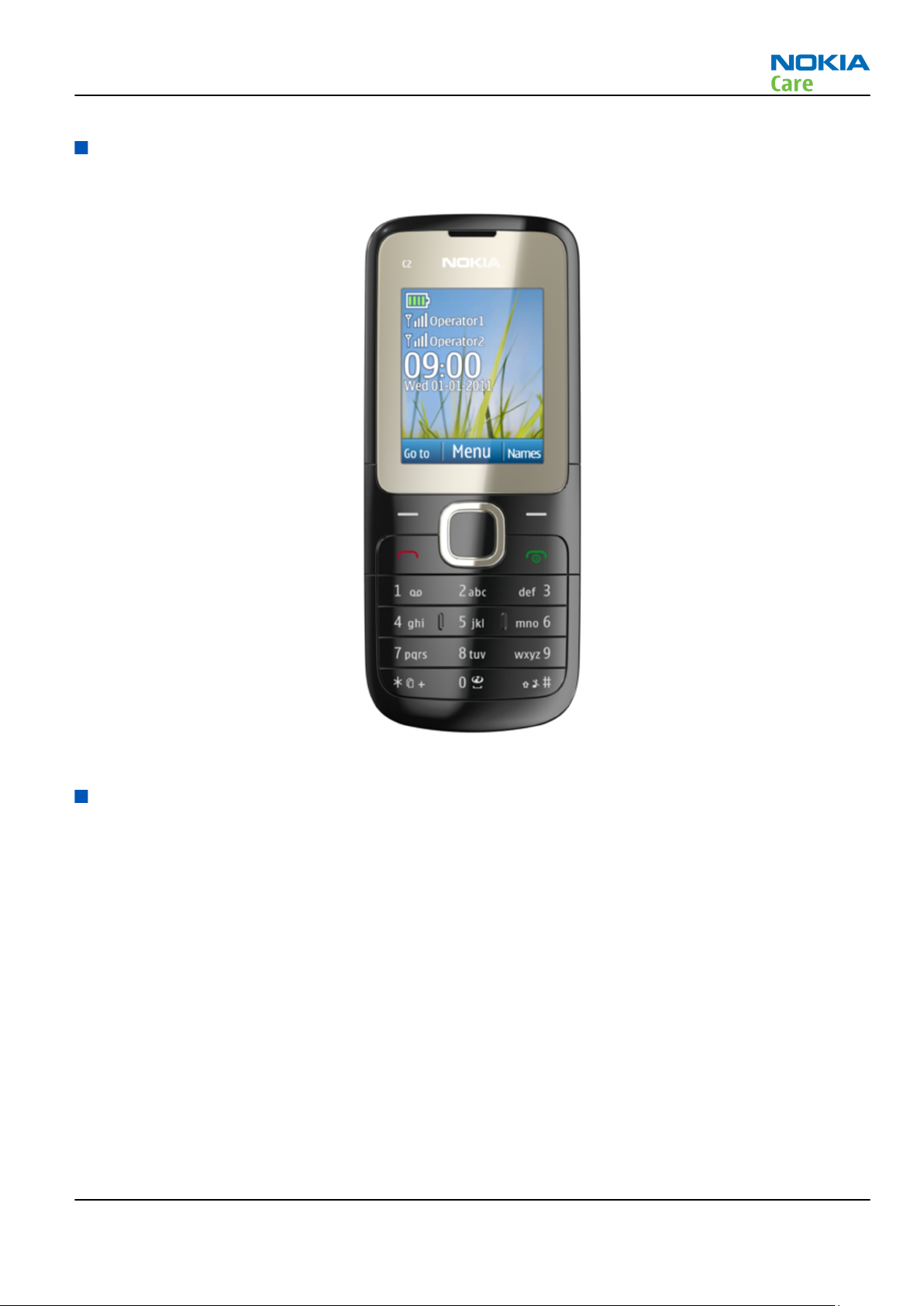
RM-704
General Information
Product selection
RM-704 (Nokia C2–00) is a GSM Quad-band phone, supporting EGSM 900/1800 bands.
Figure 1 RM-704 (Nokia C2-00) product picture
Phone features
Hardware features
•
One internal SIM slot under battery
•
One external SIM slot, hot-swap enabled
•
HW16, Dual-band variants: EGSM 900/1800 & GSM900/1800 – Edge down link only
•
Combo 32 MB Flash, 16 MB SDRAM
•
Codecs supported: FR, EFR, HR, AMR
•
SIM support: 3volt, 1.8volt
•
128x160 TFT display (ACF)
•
microSD card slot, hot-swap supported
•
VGA Camera
•
Long battery life time (BL-5C; 1020mAh)
•
Nokia AV connector
•
Stereo FM Radio & Radio recording, RDS
Issue 1 COMPANY CONFIDENTIAL Page 1 – 5
Copyright © 2011 Nokia. All rights reserved.
Page 18
•
Bluetooth
•
BTHCost4.0
•
3in1 speaker
•
Clapton microphone
•
Speaker loudness: 103db
•
3.5mm audio jack
•
Micro USB
SW features (S40 SPR10.4)
•
Smart Dual SIM, swap external SIM without rebooting
•
UI: D5, Entry S40 UI, connect UI, 3soft keys, 5way Navi™ key
•
Full MP3 player
•
Bluetooth connectivity
•
Stereo FM radio and recording
•
MP3 ringing tones
•
Java MIDP 2.1
•
OMA DRM 2.0
•
WAP 2.0
•
MMS 1.3
•
SyncML 1.2
•
Native Email Client
•
Nokia Xpress Audio messaging
•
Theme 3.0
•
Organizer with local calendar
•
Expense manager
•
Advanced calculator
•
Converter II
•
FOTA/NSU
RM-704
General Information
Applications
•
Nokia Cherry 2.5
•
Ovi Life Tool 1.7
•
Nokia Messaging service 2.0
Accessories
In-box:
•
Phone: Nokia C2–00
•
Battery: BL-5C
•
Chargers: AC-3 (China use AC-8C and CA-100C)
•
Headset: WH-102
For out-box accessories, please refer to enhancement list document.
Page 1 – 6 COMPANY CONFIDENTIAL Issue 1
Copyright © 2011 Nokia. All rights reserved.
Page 19
RM-704
General Information
Technical specifications
Transceiver general specifications
Unit Dimensions (L x W x T)
Transceiver with BL-5C
1020 mAh Li Lion
battery pack
(mm)
108 x 45 x 14.65 74.1 67.9
Weight (g)
Battery endurance
Battery Talk time Stand-by time
BL-5C with
1020 mAh Li
Lion standard
battery
Note: Variation in operation time will occur depending on SIM card, network settings and usage.
Talk time is increased by up to 30% if half rate is active and reduced by 5% if enhanced full rate is
active.
Best Talk Time ECTEL Talk Time Best Stand-by Time ECTEL Stand-by Time
11.5 hours 5.7 hours 570 hours 460 hours
Volume (cm3)
Issue 1 COMPANY CONFIDENTIAL Page 1 – 7
Copyright © 2011 Nokia. All rights reserved.
Page 20

RM-704
General Information
(This page left intentionally blank.)
Page 1 – 8 COMPANY CONFIDENTIAL Issue 1
Copyright © 2011 Nokia. All rights reserved.
Page 21

Nokia Customer Care
2 — Service Tools and Service
Concepts
Issue 1 COMPANY CONFIDENTIAL Page 2 – 1
Copyright © 2011 Nokia. All rights reserved.
Page 22
RM-704
Service Tools and Service Concepts
(This page left intentionally blank.)
Page 2 – 2 COMPANY CONFIDENTIAL Issue 1
Copyright © 2011 Nokia. All rights reserved.
Page 23

RM-704
Service Tools and Service Concepts
Table of Contents
Service tools........................................................................................................................................................... 2–5
Product specific tools....................................................................................................................................... 2–5
SS-255........................................................................................................................................................... 2–5
SS-256........................................................................................................................................................... 2–5
SS-257........................................................................................................................................................... 2–5
General tools..................................................................................................................................................... 2–5
CU-4............................................................................................................................................................... 2–6
FPS-21........................................................................................................................................................... 2–7
MJ-300 .......................................................................................................................................................... 2–8
PK-1............................................................................................................................................................... 2–8
RJ-230 ........................................................................................................................................................... 2–8
SRT-6............................................................................................................................................................. 2–8
SS-227........................................................................................................................................................... 2–9
SS-93............................................................................................................................................................. 2–9
SX-4............................................................................................................................................................... 2–9
Cables................................................................................................................................................................. 2–9
CA-101 .......................................................................................................................................................... 2–9
CA-128RS ................................................................................................................................................... 2–10
CA-31D ....................................................................................................................................................... 2–10
CA-89DS ..................................................................................................................................................... 2–10
CA-99PS...................................................................................................................................................... 2–10
PCS-1.......................................................................................................................................................... 2–11
XRS-6.......................................................................................................................................................... 2–11
Service concepts ................................................................................................................................................. 2–12
POS (Point of Sale) flash concept ................................................................................................................. 2–12
Flashing, certificate restore and product code change............................................................................. 2–13
Flashing, certificate restore, product code change and EM calibration................................................... 2–14
BB and RF tuning........................................................................................................................................... 2–15
List of Figures
Figure 2 POS flash concept ................................................................................................................................ 2–12
Figure 3 Flashing, certificate restore and product code change................................................................... 2–13
Figure 4 Flashing, certificate restore, product code change and EM calibration......................................... 2–14
Figure 5 BB and RF tuning ................................................................................................................................. 2–15
Issue 1 COMPANY CONFIDENTIAL Page 2 – 3
Copyright © 2011 Nokia. All rights reserved.
Page 24

RM-704
Service Tools and Service Concepts
(This page left intentionally blank.)
Page 2 – 4 COMPANY CONFIDENTIAL Issue 1
Copyright © 2011 Nokia. All rights reserved.
Page 25
RM-704
Service Tools and Service Concepts
Service tools
Product specific tools
The table below gives a short overview of service devices that can be used for testing, error analysis, and
repair of product RM-704. For the correct use of the service devices, and the best effort of workbench setup,
please refer to various concepts.
SS-255 Protection plate SS-255 is designed as protection plate working with SS-256 for OKI
soldering machine.
SS-256 Blowing nozzle SS-256 is a blowing nozzle which can be used with protection plates
for different soldering machines.
SS-257 Protection plate SS-257 is designed as protection plate working with SS-256 for Martin
soldering machine.
General tools
The table below gives a short overview of service devices that can be used for testing, error analysis, and
repair of product RM-704. For the correct use of the service devices, and the best effort of workbench setup,
please refer to various concepts.
Issue 1 COMPANY CONFIDENTIAL Page 2 – 5
Copyright © 2011 Nokia. All rights reserved.
Page 26
RM-704
Service Tools and Service Concepts
CU-4 Control unit CU-4 is a general service tool used with a module jig and/or a flash
adapter. It requires an external 12 V power supply.
The unit has the following features:
•
Software controlled via USB
•
EM calibration function
•
Forwards FBUS/Flashbus traffic to/from terminal
•
Forwards USB traffic to/from terminal
•
Software controlled BSI values
•
Regulated VBATT voltage
•
2 x USB2.0 connector (Hub)
•
FBUS and USB connections supported
When using CU-4, note the special order of connecting cables and
other service equipment:
Instructions
1 Connect a service tool (jig, flash adapter) to CU-4.
2 Connect CU-4 to your PC with a USB cable.
3 Connect supply voltage (12 V)
4 Connect an FBUS cable (if necessary).
5 Start service software.
Note: Service software enables CU-4 regulators via USB when
it is started.
Reconnecting the power supply requires a service software
restart.
Page 2 – 6 COMPANY CONFIDENTIAL Issue 1
Copyright © 2011 Nokia. All rights reserved.
Page 27
RM-704
Service Tools and Service Concepts
FPS-21 Flash prommer
FPS-21 sales package:
•
FPS-21 prommer
•
AC-35 power supply
•
CA-31D USB cable
FPS-21 interfaces:
Front
•
Service cable connector
Provides Flashbus, USB and VBAT connections to a mobile device.
•
SmartCard socket
A SmartCard is needed to allow DCT-4 generation mobile device
programming.
Rear
•
DC power input
For connecting the external power supply (AC-35).
•
Two USB A type ports (USB1/USB3)
Can be used, for example, for connecting external storage memory
devices or mobile devices
•
One USB B type device connector (USB2)
For connecting a PC.
•
Phone connector
Service cable connection for connecting Flashbus/FLA.
•
Ethernet RJ45 type socket (LAN)
For connecting the FPS-21 to LAN.
Inside
•
Four SD card memory slots
For internal storage memory.
Note: In order to access the SD memory card slots inside
FPS-21, the prommer needs to be opened by removing the
front panel, rear panel and heatsink from the prommer body.
Issue 1 COMPANY CONFIDENTIAL Page 2 – 7
Copyright © 2011 Nokia. All rights reserved.
Page 28
RM-704
Service Tools and Service Concepts
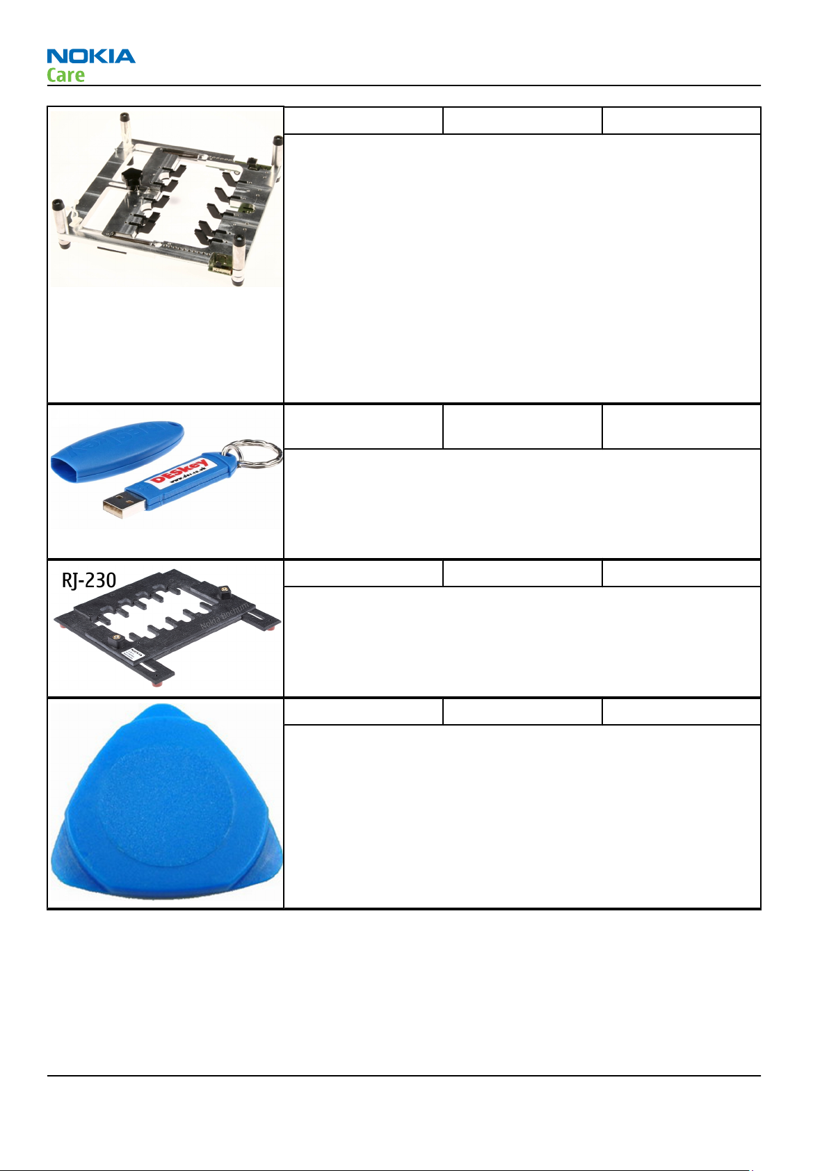
MJ-300 Module jig Module jig MJ-300 can be used for flashing via USB and RF, battery and
system testing.
The main functions are:
•
Powering with external power
•
CU-4 interface adapter to phone (requires SS-227)
•
WLAN/BT/GPS RF-interfaces with probes
•
GSM/WCDMA RF-interfaces with probes
•
BSI mode selector (Tabby and Lynx interface, selected with battery
cable)
•
VBATT interface (Tabby and Lynx interface, selected with battery
cable)
•
CA-128RS cable is used together with this jig for RF testing
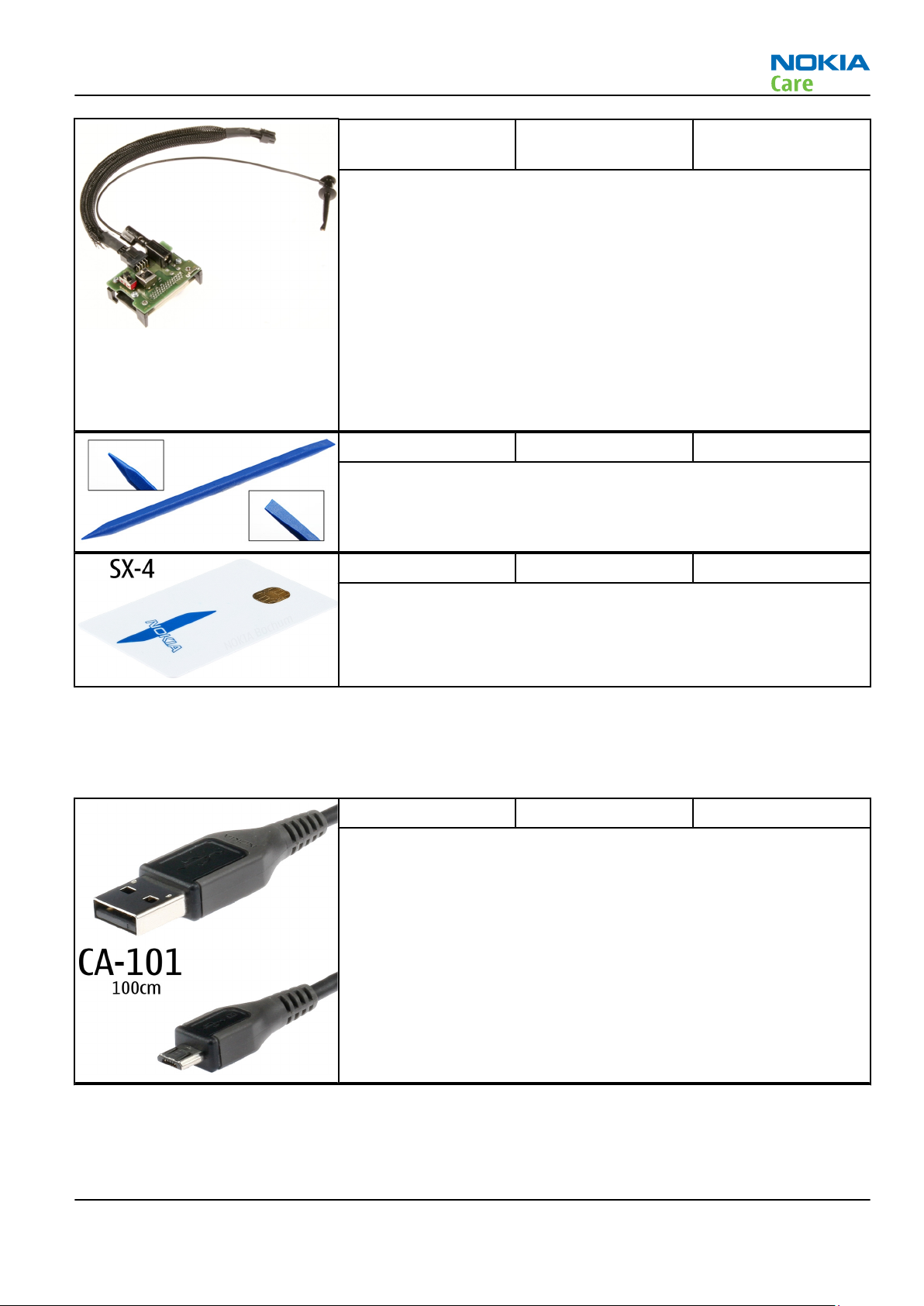
PK-1 Software protection
key
PK-1 is a hardware protection key with a USB interface. It has the same
functionality as the PKD-1 series dongle.
PK-1 is meant for use with a PC that does not have a series interface.
To use this USB dongle for security service functions please register
the dongle in the same way as the PKD-1 series dongle.
RJ-230 Soldering jig
RJ-230 is a soldering jig used for soldering and as a rework jig for the
engine module.
SRT-6 Opening tool SRT-6 is used to open phone covers.
Note: The SRT-6 is included in the Nokia Standard Toolkit.
Page 2 – 8 COMPANY CONFIDENTIAL Issue 1
Copyright © 2011 Nokia. All rights reserved.
Page 29
RM-704
Service Tools and Service Concepts
SS-227 Interface for CU-4
control unit
SS-227 is designed for regional Central Services to be able to use CU-4
with MJ-300 module jig. With SS-227, CU-4 can be used for battery
testing.
The main functions of SS-227 are:
•
CU-4 interface adapter to MJ-300
•
BSI mode selector (Lynx and Tabby mode selection)
•
VBATT interface
All functions are performed in the CU-4. Calibration voltages and
currents e.g. are protected and monitored by the CU-4 interface
software (protection for over-current, overvoltage and reverse
voltage).
SS-93 Opening tool SS-93 is used for opening JAE connectors.
Note: The SS-93 is included in Nokia Standard Toolkit.
SX-4 Smart card SX-4 is a BB5 security device used to protect critical features in tuning
and testing.
SX-4 is also needed together with FPS-21 when DCT-4 phones are
flashed.
Cables
The table below gives a short overview of service devices that can be used for testing, error analysis, and
repair of product RM-704. For the correct use of the service devices, and the best effort of workbench setup,
please refer to various concepts.
CA-101 Micro USB cable The CA-101 is a USB-to-microUSB data cable that allows connections
between the PC and the phone.
Issue 1 COMPANY CONFIDENTIAL Page 2 – 9
Copyright © 2011 Nokia. All rights reserved.
Page 30
RM-704
Service Tools and Service Concepts
CA-128RS RF tuning cable Product-specific adapter cable for RF tuning.
CA-31D USB cable The CA-31D USB cable is used to connect FPS-21 to a PC. It is included
in the FPS-21 sales package.
CA-89DS Cable Provides VBAT and Flashbus connections to mobile device
programming adapters.
CA-99PS Adapter CA-99PS adapter, 3.5 jack to 5.5 plug.
Page 2 – 10 COMPANY CONFIDENTIAL Issue 1
Copyright © 2011 Nokia. All rights reserved.
Page 31

RM-704
Service Tools and Service Concepts
PCS-1 Power cable The PCS-1 power cable (DC) is used with a docking station, a module
jig or a control unit to supply a controlled voltage.
XRS-6 RF cable The RF cable is used to connect, for example, a module repair jig to
the RF measurement equipment.
SMA to N-Connector approximately 610 mm.
Attenuation for:
•
GSM850/900: 0.3+-0.1 dB
•
GSM1800/1900: 0.5+-0.1 dB
•
WCDMA/WLAN: 0.6+-0.1dB
Issue 1 COMPANY CONFIDENTIAL Page 2 – 11
Copyright © 2011 Nokia. All rights reserved.
Page 32

Service concepts
POS (Point of Sale) flash concept
RM-704
Service Tools and Service Concepts
Figure 2 POS flash concept
Type Description
Product specific tools
BL-5C Battery
Other tools
PC with Care Suite
Cables
CA-101 Micro USB cable
Page 2 – 12 COMPANY CONFIDENTIAL Issue 1
Copyright © 2011 Nokia. All rights reserved.
Page 33

RM-704
Service Tools and Service Concepts
Flashing, certificate restore and product code change
Figure 3 Flashing, certificate restore and product code change
Type Description
Product specific devices
BL–5C Battery
Other devices
FPS-21 Flash prommer box
AC-35 Power supply
PK-1 SW security device
SX-4 Smart card
PC with service software (Phoenix)
Cables
CA-101 Micro USB cable
USB cable
Issue 1 COMPANY CONFIDENTIAL Page 2 – 13
Copyright © 2011 Nokia. All rights reserved.
Page 34

Service Tools and Service Concepts
Flashing, certificate restore, product code change and EM calibration
RM-704
Figure 4 Flashing, certificate restore, product code change and EM calibration
Type Description
Product specific tools
MJ-300 Module jig
Other tools
CU-4 Control unit
FPS-21 Flash prommer box
PK-1 SW security device
SX-4 Smart card
PC with service software (Phoenix)
Cables
CA-101 Micro USB cable
CA-89DS Service cable
CA-99PS Adapter
PCS-1 Power cable
USB cable
Page 2 – 14 COMPANY CONFIDENTIAL Issue 1
Copyright © 2011 Nokia. All rights reserved.
Page 35

RM-704
Service Tools and Service Concepts
BB and RF tuning
Figure 5 BB and RF tuning
Type Description
Phone specific devices
MJ–300 Module jig
Other devices
CU-4 Control unit
SS-227 CU-4 interface part
FPS-21 Flash prommer box
PK-1 SW security device
SX-4 Smart card
PC with service software (Care Suite)
Measurement equipment
Cables
CA-101 Micro USB cable
PCS-1 DC power cable
XRS-6 RF cable
USB cable
GPIB control cable
CA-128RS Product specific RF adapter cable
Issue 1 COMPANY CONFIDENTIAL Page 2 – 15
Copyright © 2011 Nokia. All rights reserved.
Page 36

RM-704
Service Tools and Service Concepts
(This page left intentionally blank.)
Page 2 – 16 COMPANY CONFIDENTIAL Issue 1
Copyright © 2011 Nokia. All rights reserved.
Page 37

Nokia Customer Care
3 — BB Troubleshooting and
Manual Tuning Guide
Issue 1 COMPANY CONFIDENTIAL Page 3 – 1
Copyright © 2011 Nokia. All rights reserved.
Page 38

RM-704
BB Troubleshooting and Manual Tuning Guide
(This page left intentionally blank.)
Page 3 – 2 COMPANY CONFIDENTIAL Issue 1
Copyright © 2011 Nokia. All rights reserved.
Page 39

RM-704
BB Troubleshooting and Manual Tuning Guide
Table of Contents
Baseband Troubleshooting .................................................................................................................................. 3–5
Introduction to BB Troubleshooting ................................................................................................................... 3–5
Non re-workable Baseband Components ........................................................................................................... 3–5
Baseband main troubleshooting......................................................................................................................... 3–5
........................................................................................................................................................................... 3–5
Phone does not power on............................................................................................................................... 3–6
Power supply troubleshooting ....................................................................................................................... 3–6
Clocking system troubleshooting ................................................................................................................... 3–9
Flash programming troubleshootin............................................................................................................ 3–11
Main memory troubleshooting.................................................................................................................... 3–12
Charging troubleshooting ............................................................................................................................ 3–13
SIM card troubleshooting ............................................................................................................................. 3–15
Dual SIM troubleshooting............................................................................................................................. 3–17
USB troubleshooting..................................................................................................................................... 3–18
User interface troubleshooting......................................................................................................................... 3–20
Keyboard troubleshooting ........................................................................................................................... 3–20
Display troubleshooting ............................................................................................................................... 3–21
Backlight troubleshooting............................................................................................................................ 3–22
Camera interface troubleshooting ................................................................................................................... 3–23
Camera troubleshooting instructions ......................................................................................................... 3–23
No valid data from Camera interface IC ..................................................................................................... 3–25
Audio troubleshooting....................................................................................................................................... 3–26
Audio troubleshooting test instructions..................................................................................................... 3–26
Internal microphone troubleshooting........................................................................................................ 3–27
Internal earpiece troubleshooting .............................................................................................................. 3–29
IHF speaker troubleshooting........................................................................................................................ 3–30
External microphone troubleshooting........................................................................................................ 3–31
Headset speaker troubleshooting ............................................................................................................... 3–32
FM radio troubleshooting.................................................................................................................................. 3–33
FM radio troubleshooting............................................................................................................................. 3–33
Memory card troubleshooting .......................................................................................................................... 3–35
Cannot detect memory card......................................................................................................................... 3–35
Baseband manual tuning guide........................................................................................................................ 3–35
Certificate restoring BB5............................................................................................................................... 3–35
Energy management calibration................................................................................................................. 3–39
List of Figures
Figure 6 Baseband test point locations .............................................................................................................. 3–5
Listing 1: High current when battery is inserted, I>500mA; ............................................................................ 3–7
Figure 8 High current when battery inserted..................................................................................................... 3–7
Figure 9 IR picture showing component overheat ............................................................................................ 3–7
Listing 2: High current after pressing power-on key, 100mA<I<500mA......................................................... 3–8
Figure 11 High current after pressing power-on key ........................................................................................ 3–8
Figure 12 No current when pressing power on key .......................................................................................... 3–9
Figure 13 26 MHz Clock does not work ............................................................................................................ 3–10
Figure 14 32 KHz RTC clock does not work ...................................................................................................... 3–11
Figure 15 Cannot identify charger.................................................................................................................... 3–14
Figure 16 No charging current.......................................................................................................................... 3–15
Figure 17 Cannot identify SIM card................................................................................................................... 3–15
Issue 1 COMPANY CONFIDENTIAL Page 3 – 3
Copyright © 2011 Nokia. All rights reserved.
Page 40

RM-704
BB Troubleshooting and Manual Tuning Guide
Figure 18 SIM voltages, no ATR......................................................................................................................... 3–16
Figure 19 SIM voltages, normal startup at 3V ................................................................................................. 3–16
Figure 20 SIM 1 troubleshooting flow.............................................................................................................. 3–17
Figure 21 SIM 2 troubleshooting flow.............................................................................................................. 3–18
Figure 22 Pin 3 of V2202.................................................................................................................................... 3–20
Figure 23 Blank display troubleshooting flow ................................................................................................ 3–22
Figure 24 No backlight troubleshooting flow ................................................................................................. 3–23
Figure 25 Interface signals between D3100 and N3000 ................................................................................ 3–24
Figure 26 Camera interface IC troubleshooting guide ................................................................................... 3–25
Figure 27 Phoenix audio test window............................................................................................................. 3–26
Figure 28 PWB audio test point........................................................................................................................ 3–27
Figure 29 Test arrangement for microphone.................................................................................................. 3–28
Figure 30 Internal microphone troubleshooting flow ................................................................................... 3–28
Figure 31 Test arrangement for earpiece........................................................................................................ 3–29
Figure 32 Internal earpiece troubleshooting flow ......................................................................................... 3–30
Figure 33 Test arrangement for IHF speaker................................................................................................... 3–31
Figure 34 IHF speaker troubleshooting flow................................................................................................... 3–31
Figure 35 Test arrangement for external microphone................................................................................... 3–32
Figure 36 external microphone troubleshooting flow................................................................................... 3–32
Figure 37 Test arrangement for headset speaker........................................................................................... 3–33
Page 3 – 4 COMPANY CONFIDENTIAL Issue 1
Copyright © 2011 Nokia. All rights reserved.
Page 41

RM-704
BB Troubleshooting and Manual Tuning Guide
Baseband Troubleshooting
The following sections contains guidelines how to identify and correct basic baseband related faults. Access
to normal LAB equipment (power-supply, digital multi-meter and oscilloscope) is a prerequisite for following
the guidelines. Due to the small size of the components and test-points, access to a microscope or magnifying
glass is recommended.
Introduction to BB Troubleshooting
Initial baseband troubleshooting normally involves the measurements of various power supply voltages and
control signals. The location on the most important test-points is indicated in the following figure:
Figure 6 Baseband test point locations
Non re-workable Baseband Components
The XGold 213 V2.1S GSM controller IC D3100 is non-reworkable. This means that if failure diagnostics leads
to the conclusion of defective D3100, the PWB has to be swapped with a working unit.
Baseband main troubleshooting
The following sections will contain in-depth trouble-shooting guides for various areas of the baseband circuit.
It is assumed that a battery simulator containing a valid BSI resistance is used to supply the phone, or a valid
battery is used.
Issue 1 COMPANY CONFIDENTIAL Page 3 – 5
Copyright © 2011 Nokia. All rights reserved.
Page 42

Phone does not power on
Troubleshooting flow
RM-704
BB Troubleshooting and Manual Tuning Guide
Power supply troubleshooting
High current
If the phone draws excessively high current upon power on or insertion of battery, it means that VBAT or a
LDO output is shorted.
Page 3 – 6 COMPANY CONFIDENTIAL Issue 1
Copyright © 2011 Nokia. All rights reserved.
Page 43

RM-704
BB Troubleshooting and Manual Tuning Guide
Listing 1: High current when battery is inserted, I>500mA;
Refer to the following picture:
Figure 8 High current when battery inserted
Figure 9 IR picture showing component overheat
Issue 1 COMPANY CONFIDENTIAL Page 3 – 7
Copyright © 2011 Nokia. All rights reserved.
Page 44

BB Troubleshooting and Manual Tuning Guide
Listing 2: High current after pressing power-on key, 100mA<I<500mA.
RM-704
Figure 11 High current after pressing power-on key
Page 3 – 8 COMPANY CONFIDENTIAL Issue 1
Copyright © 2011 Nokia. All rights reserved.
Page 45

RM-704
BB Troubleshooting and Manual Tuning Guide
No current when pressing power on key
Figure 12 No current when pressing power on key
Clocking system troubleshooting
26 MHz clock does not work
If the 26 MHz crystal does not work, it may be due to B7100 malfunction or a soldering defect.
Issue 1 COMPANY CONFIDENTIAL Page 3 – 9
Copyright © 2011 Nokia. All rights reserved.
Page 46

RM-704
BB Troubleshooting and Manual Tuning Guide
Figure 13 26 MHz Clock does not work
32 KHz RTC clock does not work
If the 32 KHz crystal does not work, it may be due to B3000 malfunction, matching capacitor or B3000
soldering defect.
Page 3 – 10 COMPANY CONFIDENTIAL Issue 1
Copyright © 2011 Nokia. All rights reserved.
Page 47

RM-704
BB Troubleshooting and Manual Tuning Guide
Figure 14 32 KHz RTC clock does not work
Flash programming troubleshootin
Context
Flash programming can be done via the USB test points or the USB connector. If there is a connectivity issue
(open/short circuit) under BGA chip, it may also cause programming failure. It is assumed that the integrity
of the USB connection is verified prior to flashing troubleshooting.
The Phoenix tool can give some useful information about the failure as indicated in the following
programming troubleshooting flow.
Issue 1 COMPANY CONFIDENTIAL Page 3 – 11
Copyright © 2011 Nokia. All rights reserved.
Page 48

Troubleshooting flow
RM-704
BB Troubleshooting and Manual Tuning Guide
Main memory troubleshooting
Context
Possible issues happen on the main memory could be: image corruption, soldering issue or flash chip
damaged.
Page 3 – 12 COMPANY CONFIDENTIAL Issue 1
Copyright © 2011 Nokia. All rights reserved.
Page 49

RM-704
BB Troubleshooting and Manual Tuning Guide
Troubleshooting flow
Charging troubleshooting
Can not identify charger
When inserting the wall adaptor into the phone, the phone will detect a valid voltage if charger output
voltage is 4.6 – 9.3V. But if something is wrong with the voltage detect/measurement circuit, then the phone
cannot correctly identify the charger.
Issue 1 COMPANY CONFIDENTIAL Page 3 – 13
Copyright © 2011 Nokia. All rights reserved.
Page 50

RM-704
BB Troubleshooting and Manual Tuning Guide
Figure 15 Cannot identify charger
No charging current (cannot charge battery fully in expected time)
When the phone is in constant current or constant voltage charge state, the average charging current is
controlled by phone SW. The current is feed into battery though the V2204 transistor, the phone measures
charging current by sampling the voltage over resistor R2208. If there is something wrong at this path, the
charging current may be out of specification. It is assumed that phone can detect the presence of the charger,
otherwise please refer to the above section.
Page 3 – 14 COMPANY CONFIDENTIAL Issue 1
Copyright © 2011 Nokia. All rights reserved.
Page 51

RM-704
BB Troubleshooting and Manual Tuning Guide
Figure 16 No charging current
SIM card troubleshooting
Cannot identify SIM card
The hardware of the SIM interface from XGOLD213 (D3100) to the SIM connector (X2750) can be tested without
a SIM card. When the phone is switched on, the phone first checks for a 1.8V SIM card, and then for a 3V SIM
card. The phone will try this several times, where after it will display “Insert SIM card”.
Figure 17 Cannot identify SIM card
Issue 1 COMPANY CONFIDENTIAL Page 3 – 15
Copyright © 2011 Nokia. All rights reserved.
Page 52

RM-704
BB Troubleshooting and Manual Tuning Guide
Figure 18 SIM voltages, no ATR
SIM card rejected
The error “SIM card rejected” means that the ATR message received from SIM card is corrupted, e.g. data
signal levels are wrong. The first data is always ATR and it is sent from card to phone. For reference a picture
with normal SIM power-up is shown below.
Figure 19 SIM voltages, normal startup at 3V
Page 3 – 16 COMPANY CONFIDENTIAL Issue 1
Copyright © 2011 Nokia. All rights reserved.
Page 53

RM-704
BB Troubleshooting and Manual Tuning Guide
Dual SIM troubleshooting
Troubleshooting SIM problems on a dual SIM product is very similar to the procedures outlined in the above
section. The presence of the dual SIM IC is detected by the self-test routine, and as such it can be assumed
that presence and interface towards the BB IC is verified if the self-test passes. The troubleshooting guides
will as a consequence focus on dual SIM IC <-> SIM card related problems. It also assumed that troubleshooting
on SIM1 is done using only one SIM card, which is inserted either in slot 1, and troubleshooting on SIM2 is
done using 2 SIM cards, so both slots needs to be occupied.
SIM 1 not recognized
Figure 20 SIM 1 troubleshooting flow
Issue 1 COMPANY CONFIDENTIAL Page 3 – 17
Copyright © 2011 Nokia. All rights reserved.
Page 54

SIM 2 not recognized
RM-704
BB Troubleshooting and Manual Tuning Guide
Figure 21 SIM 2 troubleshooting flow
USB troubleshooting
Context
If the phone cannot be detected by PC when the USB cable is inserted, this means that communication
between phone and PC can not be setup. This may be due to soldering issue or a malfunction in the ESD
protection device.
Page 3 – 18 COMPANY CONFIDENTIAL Issue 1
Copyright © 2011 Nokia. All rights reserved.
Page 55

RM-704
BB Troubleshooting and Manual Tuning Guide
Troubleshooting flow
Issue 1 COMPANY CONFIDENTIAL Page 3 – 19
Copyright © 2011 Nokia. All rights reserved.
Page 56

RM-704
BB Troubleshooting and Manual Tuning Guide
User interface troubleshooting
Keyboard troubleshooting
Context
One or more keys don’t function at all.
Figure 22 Pin 3 of V2202
Page 3 – 20 COMPANY CONFIDENTIAL Issue 1
Copyright © 2011 Nokia. All rights reserved.
Page 57

RM-704
BB Troubleshooting and Manual Tuning Guide
Troubleshooting flow
Display troubleshooting
Blank display
The display doesn’t show any information at all when phone is powered on. XGOLD connects the LCD via the
serial port. If the communication between XGOLD and LCD has problems, the XGOLD may be not be able to
initialize LCD correctly. The XGOLD also feeds 2 power supplies to the LCD: VAUX and 1V8, if these 2 power
supply work abnormally, the LCD also doesn’t work.
Issue 1 COMPANY CONFIDENTIAL Page 3 – 21
Copyright © 2011 Nokia. All rights reserved.
Page 58

RM-704
BB Troubleshooting and Manual Tuning Guide
Figure 23 Blank display troubleshooting flow
Display is corrupt
The display contains missing or fading segments or color presentation is incorrect. Since ACF assembling is
used, it cannot be repaired.
Backlight troubleshooting
No backlight
The backlight is driven by a DC-DC converter. The LCD backlight LED’s and the keypad LED’s are in connected
in serial path. If any component on this serial path is open circuit, there is no backlight.
Page 3 – 22 COMPANY CONFIDENTIAL Issue 1
Copyright © 2011 Nokia. All rights reserved.
Page 59

RM-704
BB Troubleshooting and Manual Tuning Guide
Figure 24 No backlight troubleshooting flow
Camera interface troubleshooting
Camera troubleshooting instructions
Camera troubleshooting involves debugging on two interfaces; the interface between the camera module
itself and the camera interface IC N3000, and debugging on the interface between N3000 and the baseband
IC D3100. Troubleshooting on interface between camera and N3000 is outside the scope of this specification.
In the following troubleshooting guide it is assumed that the integrity of this interface is already verified
and valid signal are present on the inputs of N3000.
Issue 1 COMPANY CONFIDENTIAL Page 3 – 23
Copyright © 2011 Nokia. All rights reserved.
Page 60

RM-704
BB Troubleshooting and Manual Tuning Guide
Figure 25 Interface signals between D3100 and N3000
The above figure shows the interface signals between N3000 and D3100 when the camera is active:
Yellow: Pixel Clock signal J3002
Red: Data bit 0 J3003
Green: Hsync J3005
Blue: Vsync J3006
Actual pixel clock frequency, Vsync and Hsync frequency and data content will depend on the camera used
(resolution, frame-rate) and operating mode (still picture capture, video recording, viewfinder mode).
Page 3 – 24 COMPANY CONFIDENTIAL Issue 1
Copyright © 2011 Nokia. All rights reserved.
Page 61

RM-704
BB Troubleshooting and Manual Tuning Guide
No valid data from Camera interface IC
Figure 26 Camera interface IC troubleshooting guide
Configuration of the camera interface chip IC:
CCP_CLASS_SEL = GND: SMIA Class 0, Strobe pins functions as Clock inputs (ACME VGA module)
CCP_CLASS_SEL = 1.8V: SMIA Class 1, Strobe and Data. (2MP Gandalf module)
Issue 1 COMPANY CONFIDENTIAL Page 3 – 25
Copyright © 2011 Nokia. All rights reserved.
Page 62

Audio troubleshooting
Audio troubleshooting test instructions
Audio troubleshooting using phoenix:
RM-704
BB Troubleshooting and Manual Tuning Guide
Figure 27 Phoenix audio test window
Page 3 – 26 COMPANY CONFIDENTIAL Issue 1
Copyright © 2011 Nokia. All rights reserved.
Page 63

RM-704
BB Troubleshooting and Manual Tuning Guide
Figure 28 PWB audio test point
Internal microphone troubleshooting
Steps:
1 Connect phone with Phoenix.
2 Open “audio test” window from “Testing –> Audio test”, as shown in Figure Phoenix audio test window
above.
3 Select “Hp microphone in Ext speaker out”.
Issue 1 COMPANY CONFIDENTIAL Page 3 – 27
Copyright © 2011 Nokia. All rights reserved.
Page 64

BB Troubleshooting and Manual Tuning Guide
4 Select “Loop” as “On”.
5 Input sound at microphone port, for example 94dB SPL 1kHz.
6 Check if signal is detected at HS_EAR_L/R pads, as shown in Figure “PWB audio test points” above.
Figure 29 Test arrangement for microphone
RM-704
Figure 30 Internal microphone troubleshooting flow
Page 3 – 28 COMPANY CONFIDENTIAL Issue 1
Copyright © 2011 Nokia. All rights reserved.
Page 65

RM-704
BB Troubleshooting and Manual Tuning Guide
Internal earpiece troubleshooting
Steps:
1 Connect phone with Phoenix.
2 Open “audio test” window from “Testing –> Audio test”, as shown in Figure Phoenix audio test window
above.
3 Select “Ext microphone in Hp speaker out”.
4 Select “Loop” as “On”.
5 Input signal to HS_MIC/GND pads, as shown in Figure PWB audio test point above, for example 100mVpp,
1kHz.
6 Check if sound is heard in earpiece.
Figure 31 Test arrangement for earpiece
Issue 1 COMPANY CONFIDENTIAL Page 3 – 29
Copyright © 2011 Nokia. All rights reserved.
Page 66

RM-704
BB Troubleshooting and Manual Tuning Guide
Figure 32 Internal earpiece troubleshooting flow
IHF speaker troubleshooting
Steps:
1 Connect phone with Phoenix.
2 Open “audio test” window from “Testing –> Audio test”, as shown in Figure Phoenix audio test window
above.
3 Select “Ext microphone in IHF speaker out”.
4 Select “Loop” as “On”.
5 Input signal to HS_MIC/GND pads, as shown in Figure PWB audio test point above, for example 100mVpp,
1kHz.
6 6) Check if sound is heard in IHF.
Page 3 – 30 COMPANY CONFIDENTIAL Issue 1
Copyright © 2011 Nokia. All rights reserved.
Page 67

RM-704
BB Troubleshooting and Manual Tuning Guide
Figure 33 Test arrangement for IHF speaker
Figure 34 IHF speaker troubleshooting flow
External microphone troubleshooting
Steps:
1 Connect phone with Phoenix.
2 Open “audio test” window from “Testing –> Audio test”, as shown in Figure Phoenix audio test window
above.
3 Select “Ext microphone in Ext speaker out”.
4 Select “Loop” as “On”.
5 Input sound at microphone port, for example 94dB SPL 1kHz.
6 Check if signal is detected at HS_EAR_L/R pads, shown in Figure PWB audio test points above.
Issue 1 COMPANY CONFIDENTIAL Page 3 – 31
Copyright © 2011 Nokia. All rights reserved.
Page 68

BB Troubleshooting and Manual Tuning Guide
Figure 35 Test arrangement for external microphone
RM-704
Figure 36 external microphone troubleshooting flow
Headset speaker troubleshooting
Steps:
1 Connect phone with Phoenix.
2 Open “audio test” window from “Testing –> Audio test”, as shown in Figure Phoenix audio test window
above.
3 Select “Ext microphone in Ext speaker out”.
4 Select “Loop” as “On”.
5 Input signal to HS_MIC/GND pads, as shown in Figure PWB audio test point above, for example 100mVpp,
1kHz.
6 Check if sound is heard in headset.
Page 3 – 32 COMPANY CONFIDENTIAL Issue 1
Copyright © 2011 Nokia. All rights reserved.
Page 69

RM-704
BB Troubleshooting and Manual Tuning Guide
Figure 37 Test arrangement for headset speaker
FM radio troubleshooting
FM radio troubleshooting
Context
FM radio problems can fall into two categories; not possible to tune into a station when headset cable is
inserted, or it can tune in on a station (Station ID and valid signal strength indicated in display) but there is
no audio. In the latter case please refer to “IHF speaker troubleshooting” or “Headset speaker
troubleshooting” for trouble shooting the downlink audio path and headset detection function. It is assumed
that live FM stations with sufficient signal strength are available on the point of service, and that a dedicated
FM signal generator is not used during troubleshooting.
Issue 1 COMPANY CONFIDENTIAL Page 3 – 33
Copyright © 2011 Nokia. All rights reserved.
Page 70

Troubleshooting flow
RM-704
BB Troubleshooting and Manual Tuning Guide
Page 3 – 34 COMPANY CONFIDENTIAL Issue 1
Copyright © 2011 Nokia. All rights reserved.
Page 71

RM-704
BB Troubleshooting and Manual Tuning Guide
Memory card troubleshooting
Cannot detect memory card
Context
Quantum support SD/MMC card.
Troubleshooting flow
Baseband manual tuning guide
Certificate restoring BB5
Context
This procedure is performed when the Combo Memory is replaced.
Hardware and Software Setup:
Issue 1 COMPANY CONFIDENTIAL Page 3 – 35
Copyright © 2011 Nokia. All rights reserved.
Page 72

RM-704
BB Troubleshooting and Manual Tuning Guide
•
Latest Phoenix Service Software supporting phone model
•
Latest phone model specific Data Package
•
FPS--10 or 21 Flash prommer
•
SX-4 Smart Card with Enabled Certificate Restore feature
•
Phone model specific Module Jig or Generic Module Jig
Refer to the setup in Service Concept.
Steps
1. Connect phone and scan product, read phone information to check communication with phone. Select
Tools –> Certificate Restore BB5 in the menu.
2. Provide Tucson Password and PIN code. Please note that characters are case sensitive.
3. Select OK, Phoenix will read product information from phone.
4. Product code shown on the UI does not matter, because during restoring it will be replaced by the product
code which is the latest one stored in Nokia system.
Page 3 – 36 COMPANY CONFIDENTIAL Issue 1
Copyright © 2011 Nokia. All rights reserved.
Page 73

RM-704
BB Troubleshooting and Manual Tuning Guide
5. It is recommended to perform “Restore” function without selecting “Flash Product” –– option to avoid
possible SW downgrade which causes the phone to die.
6. Information from phone and Smart Card are read and connection to Tucson server is established.
7. Information from Nokia system is retrieved and programmed in the phone.
Issue 1 COMPANY CONFIDENTIAL Page 3 – 37
Copyright © 2011 Nokia. All rights reserved.
Page 74

BB Troubleshooting and Manual Tuning Guide
8. After programming confirmation about successful event is sent to Nokia system.
RM-704
Page 3 – 38 COMPANY CONFIDENTIAL Issue 1
Copyright © 2011 Nokia. All rights reserved.
Page 75

RM-704
BB Troubleshooting and Manual Tuning Guide
Next actions
After a successful rewrite, you must retune the phone completely. (RF and BB)
Energy management calibration
Context
Energy Management calibration is performed to calibrate the settings of the AD converters in several channels
to get an accurate AD conversion result.
Hardware and Software Setup:
•
Latest Phoenix Service Software supporting phone model
•
Latest phone model specific Data Package
•
FPS--10 or 21 Flash prommer
•
Supply 12V DC from an external power supply to CU-4 to power up the phone
•
The phone must be connected to a CU-4 unit with a product-specific Module Jig or generic module jig.
Refer to the setup in Service Concept.
Steps
1. Connect CU-4 with Module Jig, and place the phone module to the Module Jig -> Mode Switch on Flashing
+ EM CALIB.
2. Start Phoenix service software.
3. Choose File -> Scan Product.
4. Choose Tuning -> Energy Management.
5. To show the current values in the phone memory, click Read.
6. Click Tune & Calculate.
Issue 1 COMPANY CONFIDENTIAL Page 3 – 39
Copyright © 2011 Nokia. All rights reserved.
Page 76

RM-704
BB Troubleshooting and Manual Tuning Guide
7. The new calibration values are shown in the calculated column. If the new calibration values seem to be
acceptable click Write to store the new calibration values to the phone permanent memory.
8. Click Read, and confirm that the new calibration values are stored in the phone memory correctly.
9. End the procedure and close the Energy Management window.
Page 3 – 40 COMPANY CONFIDENTIAL Issue 1
Copyright © 2011 Nokia. All rights reserved.
Page 77

Nokia Customer Care
4 — RF Troubleshooting
Issue 1 COMPANY CONFIDENTIAL Page 4 – 1
Copyright © 2011 Nokia. All rights reserved.
Page 78

RM-704
RF Troubleshooting
(This page left intentionally blank.)
Page 4 – 2 COMPANY CONFIDENTIAL Issue 1
Copyright © 2011 Nokia. All rights reserved.
Page 79

RM-704
RF Troubleshooting
Table of Contents
Introduction to RF Troubleshooting.................................................................................................................... 4–5
Non re-workable RF Components........................................................................................................................ 4–5
Maintenance Overview.......................................................................................................................................... 4–5
........................................................................................................................................................................... 4–5
Maintenance step 1.......................................................................................................................................... 4–6
Maintenance step 2.......................................................................................................................................... 4–6
Maintenance step 3.......................................................................................................................................... 4–6
Maintenance step 4.......................................................................................................................................... 4–7
Maintenance working flow................................................................................................................................... 4–7
Overview ........................................................................................................................................................... 4–7
Case 1: All Self Tests Passed ............................................................................................................................ 4–7
Case 2: X-Tal, Antenna detection and FEM ID Self-Test Failed...................................................................... 4–7
Case 3: RF Internal Loopback failure .............................................................................................................. 4–8
Maintenance step 1—Self test ............................................................................................................................. 4–8
Maintenance step 1 — Self test ...................................................................................................................... 4–8
Maintenance step 2 –Debugging and troubleshooting..................................................................................... 4–9
Maintenance step 2 –Debugging and troubleshooting................................................................................ 4–9
Visual inspection check flow........................................................................................................................... 4–9
RF Troubleshooting: X-Tal debug check flow............................................................................................. 4–10
RF Troubleshooting: Antenna detection check flow.................................................................................. 4–11
RF Troubleshooting: AFC troubleshooting.................................................................................................. 4–12
Receiver troubleshooting............................................................................................................................. 4–13
Receiver troubleshooting overview ....................................................................................................... 4–13
RX LB troubleshooting ............................................................................................................................. 4–14
RX HB troubleshooting............................................................................................................................. 4–18
Transmitter troubleshooting ....................................................................................................................... 4–19
Transmitter troubleshooting overview ................................................................................................. 4–19
TX LB troubleshooting ............................................................................................................................. 4–21
TX HB troubleshooting............................................................................................................................. 4–24
Maintenance step 3- Local mode verification and calibration ...................................................................... 4–26
Maintenance step 3- local mode verification and calibration .................................................................. 4–26
Maintenance step 4 –Signalling mode test...................................................................................................... 4–27
Maintenance step 4 –Signalling mode test................................................................................................. 4–27
NOKIA CARE SUITE Testing and Tuning Tool..................................................................................................... 4–27
General ........................................................................................................................................................... 4–27
General ...................................................................................................................................................... 4–27
Preparation.................................................................................................................................................... 4–28
Preparation............................................................................................................................................... 4–28
Installation..................................................................................................................................................... 4–29
Installation................................................................................................................................................ 4–29
Install testing and tuning tool................................................................................................................ 4–29
Launching Care Suite Testing and tuning Tool .......................................................................................... 4–35
You can launch Care Suite in the following ways: ................................................................................ 4–35
Layout........................................................................................................................................................ 4–36
Configuration of testing and tuning tools.................................................................................................. 4–40
Configure connections between phone and PC .................................................................................... 4–40
Preferences ............................................................................................................................................... 4–41
RF tuning........................................................................................................................................................ 4–45
................................................................................................................................................................... 4–45
RF testing ....................................................................................................................................................... 4–48
Issue 1 COMPANY CONFIDENTIAL Page 4 – 3
Copyright © 2011 Nokia. All rights reserved.
Page 80

RM-704
RF Troubleshooting
................................................................................................................................................................... 4–48
EM calibration ................................................................................................................................................ 4–49
................................................................................................................................................................... 4–49
Notes............................................................................................................................................................... 4–49
................................................................................................................................................................... 4–49
Bluetooth Troubleshooting............................................................................................................................... 4–49
Bluetooth functional description................................................................................................................. 4–49
Block diagram................................................................................................................................................ 4–50
Interface signals............................................................................................................................................ 4–51
Component placement ................................................................................................................................. 4–52
Symptom, Problem and Repair Solution..................................................................................................... 4–53
Test Coverage ................................................................................................................................................ 4–54
Test Procedure............................................................................................................................................... 4–54
Bluetooth troubleshootin............................................................................................................................. 4–56
List of Tables
Table 1 Power supply voltages for the X-GOLD213 IC RF sub-system ........................................................... 4–16
Table 2 Bluetooth Signal List............................................................................................................................. 4–51
List of Figures
Figure 38 D3100 is the non-reworkable components on PWB......................................................................... 4–5
Figure 39 RX checkpoints and component overview (measurement point marked with blue) ................ 4–14
Figure 40 X-Gold RX pin volts @ L7100(LB) / L7101(HB) ................................................................................ 4–15
Figure 41 RX LB FEM logic waveform (C1:VC1; C2:VC2; C3:VC3) ...................................................................... 4–16
Figure 42 X-Gold RX pin volts @ L7100(LB) / L7101(HB) ................................................................................ 4–18
Figure 43 TX checkpoints and component overview (measurement point marked with blue) ................ 4–20
Figure 44 X-Gold TX pin volts @ C7108(LB) /C7109 (HB)................................................................................. 4–21
Figure 45 RX LB FEM logic waveform (C1:VC1; C2:VC2; C3:VC3) ...................................................................... 4–22
Figure 46 TX LB VPC logic waveform-PCL5 (C1: VPC; C2: PAEN) ...................................................................... 4–23
Figure 47 TX HB FEM logic waveform (C1:VC1; C2:VC2; C3:VC3)...................................................................... 4–24
Figure 48 TX HB VPC logic waveform-PCL0 (C1: VPC; C2: PAEN)...................................................................... 4–25
Figure 49 Bluetooth block diagram.................................................................................................................. 4–51
Figure 50 Test points in Archie Bluetooth ASIC circuit – BTHCost4.0D (CSR8810)........................................ 4–53
Page 4 – 4 COMPANY CONFIDENTIAL Issue 1
Copyright © 2011 Nokia. All rights reserved.
Page 81

RM-704
RF Troubleshooting
Introduction to RF Troubleshooting
For the RF troubleshooting, generally 2 types of measurements are used: RF measurements and LF
measurements.
RF measurements are done with a spectrum analyzer (or spectrum analyzer alike?) and a high-frequency
probe, e.g. Agilent E4440A. Note that the test jig has some losses, which must be taken into consideration
when calibrating the test system.
LF (low frequency) and DC measurements should be done with a 10:1 probe and an oscilloscope. The probe
used in the following is a 10mW/10pF probe. For the other types of probes the voltages displayed may be
slightly different. Always make sure the measurement setup is calibrated when measuring RF parameters on
the antenna pad. When re-aligning the phone, the loss in the module repair jig should be included.
Most RF semiconductors are static discharge sensitive, i.e. ESD protection must be added during repair
(ground straps and ESD soldering irons). The FEM and the X-GOLD213 are also sensitive to moisture, i.e. these
parts must be pre-baked prior to soldering.
Key components are described in this document but there are also a lot of discrete components (resistors,
inductors and capacitors) where the troubleshooting is done by checking if soldering of the component is
done properly and checking if the component is missing from PWB. Capacitors can be checked for shortcircuiting and resistors for value by means of an Ohm meter. However it should be noted that in-circuit
measurements should be evaluated carefully.
Non re-workable RF Components
The non-reworkable component for the Quantum is the X-GOLD213 (D3100). All other components are reworkable.
Figure 38 D3100 is the non-reworkable components on PWB
Maintenance Overview
When the phone is received at the service centre, it is fully assembled, and it is the objective to identify the
failure area in the phone by doing fast troubleshooting and then locate the failed component(s). Since the
X-Gold213 IC is a non-replaceable component, it should be the primary task to identify whether the failure
is related to this component or not. In case of failure of the X-GOLD213 the current PCB will be replaced by a
new fully mounted PCB. The intention of the troubleshooting procedure is to find the failing component(s).
After this a re-tuning + verification of the phone is needed in order to secure passes of all RF parameters and
no more failures will be present.
Issue 1 COMPANY CONFIDENTIAL Page 4 – 5
Copyright © 2011 Nokia. All rights reserved.
Page 82

RM-704
RF Troubleshooting
Before sending the phone back to the customers a short verification step in normal mode + live network call
will be performed.
The Maintenance steps can be seen in the figure below:
Maintenance step 1
Step 1 is where the phone (MS) is fully assembled, i.e. the RF production connector cannot be used. The
purpose is to perform a quick identification of the failure mode using MS self test. The self-test feature will
not be able to detect the failed component, but in best case it can detect the failure area/functionality. Note
that the self test might not catch all failures.
Purpose of step 1:
•
Fast identification of any failures when phone is assembled;
•
To identify the area of the failures in order to give the operator (Service maintenance operator) further
information where to debug. (Note: Self-test will not be able to specify which component(s) is failing only
which functionality is failing.)
Maintenance step 2
Step 2 is where the phone (MS) is disassembled and the RF production connector can be used, i.e. the antenna
is not mounted. The purpose of this step is to identify the failing component(s) and replace it. In this step
the troubleshooting will be made.
Purpose of step 2:
•
Identify the failure when phone is disassembled;
•
Troubleshooting in order to find the specific failing component(s) and replace it/them.
Maintenance step 3
The Maintenance Step 3 is the local mode verification step. Note that this can be used for both troubleshooting
and verification.
Purpose of step 3:
•
In case of the MS self-test performed in Maintenance Step 1 didn’t show any errors the verification should
identify where the error is located (on functional level);
•
In case a component(s) has been replaced after troubleshooting, this step should verify that the phone
can pass all RF test after recalibration or:
a Identify if the replaced components was the component(s) causing the failure.
a Detect if other failures are present after replacing.
•
To make a final calibration and verification (local mode) to make sure that the phone passes all RF limits
and requirements.
Page 4 – 6 COMPANY CONFIDENTIAL Issue 1
Copyright © 2011 Nokia. All rights reserved.
Page 83

RM-704
RF Troubleshooting
Maintenance step 4
In Maintenance step 4 the phone will be assembled and a short test in signalling mode in order to verify that
the assembled phone with full mechanic and antenna can pass finial UI requirements in Normal Mode, i.e.
Signalling Mode and if the phone is able to do a voice call.
Purpose of step 4:
•
Finial verification step using normal mode of the full assembled phone before sending it back to the
customer;
•
To verify the phone is working in live network.
Maintenance working flow
Overview
The Maintenance step 1 is the maintenance step where all self-tests are performed on the fully assembled
MS. In some case the Self-tests will detect failure i.e. tell the maintenance operator where to debug. However
in other cases the Self-test will not detect any failure however this doesn’t mean that a failure is present. In
order to locate the area of the failure it’s recommended to run verification test (Maintenance step 3) in order
to give the Maintenance operator better hint where to trouble shoot.
Below is the different working flow described depending on outcome of the different Self-tests.
Case 1: All Self Tests Passed
Below is the working flow for the case where all Self-test passed illustrated.
The phone passes all the Self-tests meaning that the Self-Test was not able to detect any failure – however
it must be assumed that a failure is present.
In order to locate the area of the failure, the RF verification in Maintenance step 3 need to be executed. The
verification step will highlight in which area the failure is present and where to start to troubleshoot.
Debugging and troubleshooting are described in the Maintenance Step 2.
After the troubleshooting i.e. finding and replacing the failing components(s) the next step is to re-tune
(calibrate) and do RF verification (Maintenance step 3). This is done in order to secure that all failures have
been removed and no further failures are present. The MS passes needs to pass all RF related test. Finally the
MS is assembled in Maintenance step 4 and verified in normal mode.
Case 2: X-Tal, Antenna detection and FEM ID Self-Test Failed
Below is the working flow illustrated for the case where all Self-test fails the X-Tal, Antenna detection or FEM
ID Self-test in the Maintenance step.
Issue 1 COMPANY CONFIDENTIAL Page 4 – 7
Copyright © 2011 Nokia. All rights reserved.
Page 84

RM-704
RF Troubleshooting
Debug and troubleshooting should be performed in the area of the Self-test failure i.e. if it is the X-tal selftest that fails then do the X-Tal troubleshooting etc. After the troubleshooting i.e. finding and replacing the
failing components(s) the next step is to re-tune (calibrate) and do RF verification (Maintenance step 3). This
is done in order to secure that all failures have been removed and no further failures are present. The MS
passes needs to pass all RF related test. Finally the MS is assembled in Maintenance step 4 and verified in
normal mode.
Case 3: RF Internal Loopback failure
Below is the working flow described in the case where the phone fails at RF internal loop back self-test in
the Maintenance step 1.
The Internal Loop Back Self-test is a special test mode where the TX part of the X-GOLD213 is configured to
transmit on a RX frequency. This signal is weak amplified in the PA of the FEM and by the antenna switch of
the FEM directed to the RX port (not the antenna port as normal operation!) and then looped back to the RX
input of the X-GOLD213. The receiver of the X-GOLD213 is then able to measure how much of the transmitted
output power is looped back.
Since a fail in the RF loopback test can be a failure in the TX or RX (LB or HB) and the RF internal loopback selftest is not able to highlight this, it is recommended to do a verification step in the maintenance step 3 – with
the only purpose to get the info if the failure is in the TX or RX path.
After troubleshooting i.e. finding and replacing the failing components(s) the next step is to re-tune
(calibrate) and do RF verification (Maintenance step 3). This is done in order to secure that all failures have
been removed and no further failures are present. The MS passes needs to pass all RF related test. Finally the
MS is assembled in Maintenance step 4 and verified in normal mode.
Maintenance step 1—Self test
Maintenance step 1 — Self test
Run all self-tests in order to clarify if the Self-Test can detect any failures.
Page 4 – 8 COMPANY CONFIDENTIAL Issue 1
Copyright © 2011 Nokia. All rights reserved.
Page 85

RM-704
RF Troubleshooting
Maintenance step 2 –Debugging and troubleshooting
Maintenance step 2 –Debugging and troubleshooting
In this stage the phone is disassembled. The goal of this step is to identify the failed component(s) either by
visual inspection or by troubleshooting.
Visual inspection check flow
The purpose of the visual inspection is to try by visual to identify the area or component of root cause i.e.
locate burned components (mal colure), destroyed components, misplaced components and other visual
abnormalities.
Issue 1 COMPANY CONFIDENTIAL Page 4 – 9
Copyright © 2011 Nokia. All rights reserved.
Page 86

RM-704
RF Troubleshooting
Page 4 – 10 COMPANY CONFIDENTIAL Issue 1
Copyright © 2011 Nokia. All rights reserved.
Page 87

RM-704
RF Troubleshooting
RF Troubleshooting: X-Tal debug check flow
Issue 1 COMPANY CONFIDENTIAL Page 4 – 11
Copyright © 2011 Nokia. All rights reserved.
Page 88

RF Troubleshooting: Antenna detection check flow
RM-704
RF Troubleshooting
Page 4 – 12 COMPANY CONFIDENTIAL Issue 1
Copyright © 2011 Nokia. All rights reserved.
Page 89

RM-704
RF Troubleshooting
RF Troubleshooting: AFC troubleshooting
Receiver troubleshooting
Receiver troubleshooting overview
If the phone failure identified at maintenance step1&3 is indicating failure at the receiver, RX troubleshooting
must be executed.
Abbreviation and terms:
Specific abbreviations used in RX troubleshooting workflow are described here:
Abbreviation Definition
RXLB_MN C7115, L7100, C7126
RXHB_MN C7114, L7101, C7129
FEM_RxCtl VC1, VC2, VC3,
FEM_RxCtrlRes R7106, R7110, R7113
FEM_RxCtrlCap C7107, C7110, C7132
FEM_BatComp L7707, C7135, C7125, C7117, C7111
Issue 1 COMPANY CONFIDENTIAL Page 4 – 13
Copyright © 2011 Nokia. All rights reserved.
Page 90

RM-704
RF Troubleshooting
Figure 39 RX checkpoints and component overview (measurement point marked with blue)
RX LB troubleshooting
The test signal from GSM tester must be a continuous signal, as the phone has no means of synchronizing to
a GSM burst signal in local mode. To excite the RSSI detector in the same way a modulated GSM signal does,
the test signal must either be GMSK modulated (Pseudo-random bit sequence (PRBS)) or an un-modulated
CW-signal with 67.7kHz offset from center frequency.
Page 4 – 14 COMPANY CONFIDENTIAL Issue 1
Copyright © 2011 Nokia. All rights reserved.
Page 91

RM-704
RF Troubleshooting
Issue 1 COMPANY CONFIDENTIAL Page 4 – 15
Copyright © 2011 Nokia. All rights reserved.
Page 92

RM-704
RF Troubleshooting
Figure 40 X-Gold RX pin volts @ L7100(LB) / L7101(HB)
Figure 41 RX LB FEM logic waveform (C1:VC1; C2:VC2; C3:VC3)
Table 1 Power supply voltages for the X-GOLD213 IC RF sub-system
Name Ball No. Test point Function
VBAT G14 C7134 3.6V typ. Battery voltage, supply
voltage of D2B LDO
VDDRF2 G13 C7106 2.5V D2B output voltage, part of RF
supply
Page 4 – 16 COMPANY CONFIDENTIAL Issue 1
Copyright © 2011 Nokia. All rights reserved.
Page 93

RM-704
RF Troubleshooting
Name Ball No. Test point Function
VRF1 H10 C7121 1.8V DCDC output voltage, supply of
1.3V LDOs
VDDTRX B14 C7124 1.4V Transceiver supply
VDDTDC B12 C7131 1.3V VDD for Time to Digital
Converter of DPLL
VDDMS H13 C7123 1.3V Mixed signal supply
VDDXO E11 C7130 1.3V DCXO supply
VDDMMD A12 NONE 1.3V VDD for Multi Modulus Divider of
DPLL
Issue 1 COMPANY CONFIDENTIAL Page 4 – 17
Copyright © 2011 Nokia. All rights reserved.
Page 94

RX HB troubleshooting
RM-704
RF Troubleshooting
Page 4 – 18 COMPANY CONFIDENTIAL Issue 1
Copyright © 2011 Nokia. All rights reserved.
Page 95

RM-704
RF Troubleshooting
Figure 42 X-Gold RX pin volts @ L7100(LB) / L7101(HB)
Transmitter troubleshooting
Transmitter troubleshooting overview
If the phone failure identified at maintenance step1&3 is transmitter fail, and then the phone should be set
to the TX check mode, and then follow the corresponding workflow below for troubleshooting.
Abbreviation and terms:
Specific abbreviations used in TX troubleshooting workflow are described here:
Abbreviation Definition
TXLB_PI_ATT R7107, R7112, R7105
TXHB_PI_ATT R7104, R7108, R7103
TXLB_H4FILTER C7108, C7120, L7504
TXHB_H2FILTER C7109, C7101, L7106
FEM_TxCtl VC1,VC2, VC3, PAEN
FEM_TxCtrlRes R7106, R7110, R7113,R7100
FEM_TxCtrlCap C7105, C7107, C7110,C7132
FEM_BatComp L7707, C7135, C7125, C7117, C7111
Issue 1 COMPANY CONFIDENTIAL Page 4 – 19
Copyright © 2011 Nokia. All rights reserved.
Page 96

RM-704
RF Troubleshooting
Figure 43 TX checkpoints and component overview (measurement point marked with blue)
Page 4 – 20 COMPANY CONFIDENTIAL Issue 1
Copyright © 2011 Nokia. All rights reserved.
Page 97

RM-704
RF Troubleshooting
TX LB troubleshooting
Issue 1 COMPANY CONFIDENTIAL Page 4 – 21
Copyright © 2011 Nokia. All rights reserved.
Page 98

Figure 44 X-Gold TX pin volts @ C7108(LB) /C7109 (HB)
RM-704
RF Troubleshooting
Figure 45 RX LB FEM logic waveform (C1:VC1; C2:VC2; C3:VC3)
Page 4 – 22 COMPANY CONFIDENTIAL Issue 1
Copyright © 2011 Nokia. All rights reserved.
Page 99

RM-704
RF Troubleshooting
Figure 46 TX LB VPC logic waveform-PCL5 (C1: VPC; C2: PAEN)
Issue 1 COMPANY CONFIDENTIAL Page 4 – 23
Copyright © 2011 Nokia. All rights reserved.
Page 100

TX HB troubleshooting
RM-704
RF Troubleshooting
Page 4 – 24 COMPANY CONFIDENTIAL Issue 1
Copyright © 2011 Nokia. All rights reserved.
 Loading...