

Page 1

Nokia Customer Care
2505 (RM-307)
Mobile Terminal
Baseband Description and
Troubleshooting
Issue 1 04/2007 Company Confidential © 2007 Nokia Corporation
Page 2

2505 (RM-307)
Baseband Description and Troubleshooting
Contents Page
Introduction............................................................................................................... 3
Baseband and Power Management Architecture .................................................... 4
Power Up and Reset ................................................................................................ 5
Power Up .......................................................................................................6
Power Off.......................................................................................................7
Power Consumption and Operation Modes ...................................................7
Power Distribution .................................................................................................... 8
Clock Distribution...................................................................................................... 9
System Clocks .............................................................................................10
TCXO........................................................................................................... 11
SLEEP Crystal Circuit for 32.768 kHz..........................................................12
SBI CLK Interface ........................................................................................14
Flash Programming Error Description.................................................................... 14
Charging Operation ................................................................................................ 15
Battery .........................................................................................................15
Charging Circuitry ........................................................................................15
Charger Detection........................................................................................16
Charge Control ............................................................................................17
Audio ...................................................................................................................... 17
Display and Keyboard ............................................................................................ 18
Accessories ............................................................................................................ 18
Charging ......................................................................................................19
Headset Detection .......................................................................................19
RUIM CARD ........................................................................................................... 19
Test Points – Top ................................................................................................... 20
Troubleshooting...................................................................................................... 22
Mobile Terminal is Dead...............................................................................23
Flash Faults .................................................................................................24
Power Does Not Stay ON or the Mobile Terminal is Jammed ......................25
Charger Faults .............................................................................................26
Audio Faults.................................................................................................27
Display Faults ..............................................................................................31
Keypad Faults..............................................................................................32
Keypad Faults..............................................................................................33
Page 2 © 2007 Nokia Corporation Company Confidential Issue 1 04/2007
Page 3

2505 (RM-307)
Nokia Customer Care Baseband Description and Troubleshooting
Introduction
The mobile terminal using a CDMA single mode engine (Cellular/ 800) with
Qualcomm baseband consists of the following ASICs:
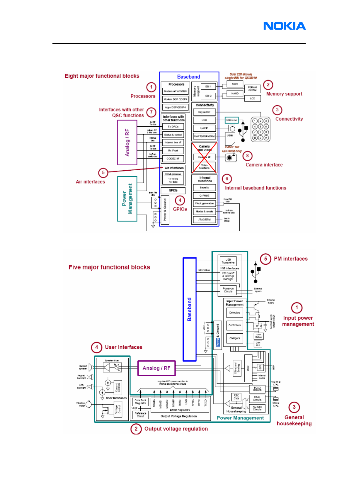
●Qualcomm Single Chip 6010, including RF transmitter and receiver,
Baseband and Power management these three categories
●64Mb Flash memory with 16Mb of Psram memory
The baseband is consisted of an Arm926EJ-S processor, a CDMA processor, two
QDSP4000 processors, Codec, Analog interface for RF and controllers for GPIOs,
UART, EBI, RUIM & peripheral interfaces, all of which are necessary to complete the
entire CDMA baseband system. The ARM926EJ-S is a high-performance, low-power
microprocessor. The features of the ARM microprocessor include a 3-stage pipelined
RISC architecture, both 32-bit ARM and 16-bit THUMB instruction sets, a 32-bit
address bus, and a 32-bit internal data bus. The two low-power, high-performance
QDSP4000 digital signal processor cores, one is for the modem (mDSP) that
dedicated to modem functions and CDMA signal processing, and the other is for
applications (aDSP) such as all vocoder functions, audio application, and CMX.
QSC6010 has two Advanced High-speed Bus (AHB),a fast peripheral bus (FPB), and
two Mobile Station Modem(MSM) bridge. Main AHB bus is controlled by the ARM926
for data and instructions. Second AHB allows mDSP and aDSP to access external
peripherals via DME interfaces. The FPB offloads the Main AHB so that a high
number of slaves does not limit its bus speed. MSM bus bridges support peripherals
that do not have an AHB interface.
The mobile terminal supports standard Nokia 2-wire and 3 wire chargers (AC-3, AC-4,
DC-4). However, the 3-wire chargers are treated as 2-wire chargers. The pulse
width modulation (PWM) controls signal for controlling the 3-wire charger is ignored.
The MSM and PM energy management software control the charging.
BL-4B (700 mAh) lithium-ion battery is used as the main power source.
Issue 1 04/2007 © 2007 Nokia Corporation Company Confidential Page 3
Page 4
2505 (RM-307)
Baseband Description and Troubleshooting
Baseband and Power Management Architecture
Figure 1: Baseband Diagram
Figure 2: Power Management of QSC6010
Page 4 © 2007 Nokia Corporation Company Confidential Issue 1 04/2007
Page 5

2505 (RM-307)
Nokia Customer Care Baseband Description and Troubleshooting
Power Up and Reset
The QSC6010 controls the power up and reset. The baseband can power up in the
following ways:
z Pressing the Power button, which means to ground the KPD_PWR_N
(“PHONE_ON_N” pin in 2505 schematic) pin of the QSC6010
z Connecting the charger to the charger input.
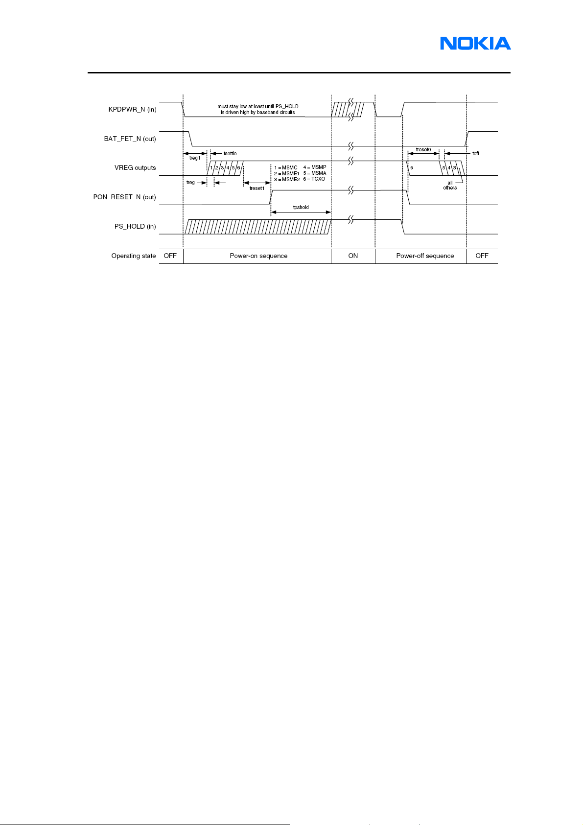
After receiving one of the above signals, the PM will start to enter reset mode. The
watchdog starts, and if the battery voltage is greater than its threshold (3V), a 6ms
delay starts to allow MSM to settle. After this delay elapses, the VERG_MSMC
regulator enables. Then, VERG_MSMP, VERG_MSMA & VERG_TCXO regulators
are enabled in sequence after MSMC. There is a 120us (4 Sleep_Clocks) delays
between each regulator’s turn on. The PON_RESET_N (“RESIN_N” pin in 2505
schematic) line holds low for another 20ms and is sent to MSM. Resets are
generated for the MSM’s internal MCU and its internal DSP, and MSM sends
TCXO_ON (“TCXO_EN” pin in 2505 schematic) signal to PM to enable TCXO. After
PON_RESET_N goes high, MSM holds PS_HOLD at low state for 200ms and then
drives PS_HOLD to high state. This will keep all regulators at on state in order to
complete this power on sequence. KPD_PWR_N key can be released after
PS_HOLD goes high.
The RESOUT_N from QSC6010 is used to reset flash memory during power up and
to put the flash memory in power down during sleep mode. LCD_RS from QSC6010
is used to reset LCD module during power up. All baseband regulators are switched
on when the PM is powered on. The QSC6010’s internal watchdog runs and resets
during normal operation. If the watchdog expires, it will generate a reset signal to
reset to MSM status. Then, QSC6010 drives RESOUT_N and LCD_RS low to reset
flash memory and LCD module.
Figure 3 represents the PM start-up sequence from reset to power-on.
Issue 1 04/2007 © 2007 Nokia Corporation Company Confidential Page 5
Page 6
2505 (RM-307)
Baseband Description and Troubleshooting
Figure 3: Power-on & off sequence and timing
Power Up
The mobile terminal can use the power key or a charger to power up.
Power Key
When the power key is pressed, the PM enters the power-up sequence. Pressing the
power key causes the KPD_PWR_N (PHONE_ON_N pin in 2505 schematic) pin to
GND. The KPD_PWR_N signal is not part of the keypad matrix. The power key is
only connected to the PM. This means that when the power key is pressed, an
interrupt will be generated to the MSM in order to power on the MCU. The MCU
reads the QSC6010’s interrupt register and notifies that it is a KPD_PWR_N interrupt.
The MCU reads the status of the KPD_PWR_N signal using the control bus. If the
KPD_PWR_N signal stays low for a certain time, the MCU accepts this as a valid
power-on state and continues with the software baseband initialization. If the power
key does not indicate a valid power-on situation, the MCU powers off the baseband.
Charger
Charging is controlled by start-up charging circuitry in order to detect and start
charging in cases the main battery is empty and the PM has no supply.
External Supply Source is Detected
If a valid source is applied to VCHG (pin V15 of QSC6010) and the battery voltage of
VPH_PWR exceeds PM’s valid UVLO (2.5V) threshold, the power-on sequence of
PM is initiated and enables its internal regulators. UVLO is the minimum voltage
required for QSC6010 operation. If the entire power-on sequence is successful, the
appropriate interrupt from PM will be sent to the MSM. Once the battery voltage rises
Page 6 © 2007 Nokia Corporation Company Confidential Issue 1 04/2007
Page 7

2505 (RM-307)
Nokia Customer Care Baseband Description and Troubleshooting
above 3.0V (min. MSM operation voltage), code start running on MSM. The MSM
reads PM registers to identify the power source and whether battery charging is
required. If a valid supply voltage is applied while the PM is on, the power-on
sequence is skipped. A charging sequence will then be initiated.
Power Off
While the PS_HOLD signal from the MSM is high, and the PM is in one of its
power-on states. Under this condition, the PM continually monitors three events that
could trigger a power-off sequence:
z
The MSM drives the PS_HOLD signal low responding to the pressing of the
keypad power button.
z Battery voltage drops below power off threshold (Battery voltage < 3.2 V).
z The PM die temperature exceeds its “severe” over-temperature threshold.
Power Consumption and Operation Modes
Power-off Mode
In power-off mode, power (VPH_PWR) is supplied to the PM, RF PA, vibrator, and
keypad backlight LED. During this mode, the current consumption is approximately
8.8 uA.
Sleep Mode
The mobile terminal enters sleep mode only when MSM makes the request to PM
through the SBI bus. PM then enters Power Saving Mode, and the VREG_MSMC
VREG_MSMP regulators remain in power-on stage. The 32.768 kHz crystal is
enabled. TCXO buffers are off. All other functions and regulators are controlled
individually via SBI and are typically disabled for minimum power dissipation.
It exits the Sleep mode either by the expiration of a sleep clock counter in the PM or
by some external interrupt (generated by a charger connection, key press, headset
connection, etc.). The TCXO is shut down in sleep mode and the 32.768 kHz sleep
clock oscillator is used as a reference clock for the baseband.
Active Mode
In active mode, the mobile terminal operates normally. It scans channels, listens to a
base station, transmits and processes information. There are several sub-states
under the active mode. Depending on the mobile terminal’s current state, there are
states such as burst reception, burst transmission, etc.
Issue 1 04/2007 © 2007 Nokia Corporation Company Confidential Page 7
Page 8

2505 (RM-307)
Baseband Description and Troubleshooting
In active mode, this is a normal operating mode for PM. VREG_MSMC,
VREG_MSMP, VREG_MSMA, VREG_RUIM, VREG_RFRX, VREG_RFTX, and
VREG_TCXO regulators are all turned on. TCXO oscillator is enabled, and TCXO
buffers are turned on. All other functions and regulators are controlled individually via
SBI.
Charging Mode
Charging mode can function in parallel with any other operating mode. A BSI resistor
inside the battery pack indicates the battery type/ size. The resistor value
corresponds to a specific battery capacity. The PM measures the battery voltage,
temperature, size, and charging current.
Charger control block inside the PM controls the charging current delivered from the
charger to the battery and mobile terminal. The maximum battery voltage is limited
by turning the PM switch off when the battery voltage reaches 4.2 V. The charging
current is monitored by measuring the voltage drop across a 0.1 ohm resistor.
Power Distribution
In normal operation, the baseband is powered by the mobile terminal‘s battery pack.
The battery pack consists of one lithium-ion cell with a capacity of 820 mAh and
safety and protection circuits.
The PM controls the power distribution to the whole mobile terminal, which includes
the baseband and the RF regulators, but excludes the RF power amplifier (RF PA)
RF power amplifier drains power from the battery directly. The battery provides
power directly to the following parts of the system:
z PM
z RF PA
z Vibrator
z Keyboard , Electric torch light& LCD backlights
The heart of the power distribution is the power control block inside the PM. It
includes all the voltage regulators and feeds the power to the entire system. The PM
handles hardware power-up functions so that the regulators are not powered on and
the power up reset (PURX) is not released if the battery voltage is less than 3 V.
Page 8 © 2007 Nokia Corporation Company Confidential Issue 1 04/2007
Page 9
2505 (RM-307)
Nokia Customer Care Baseband Description and Troubleshooting
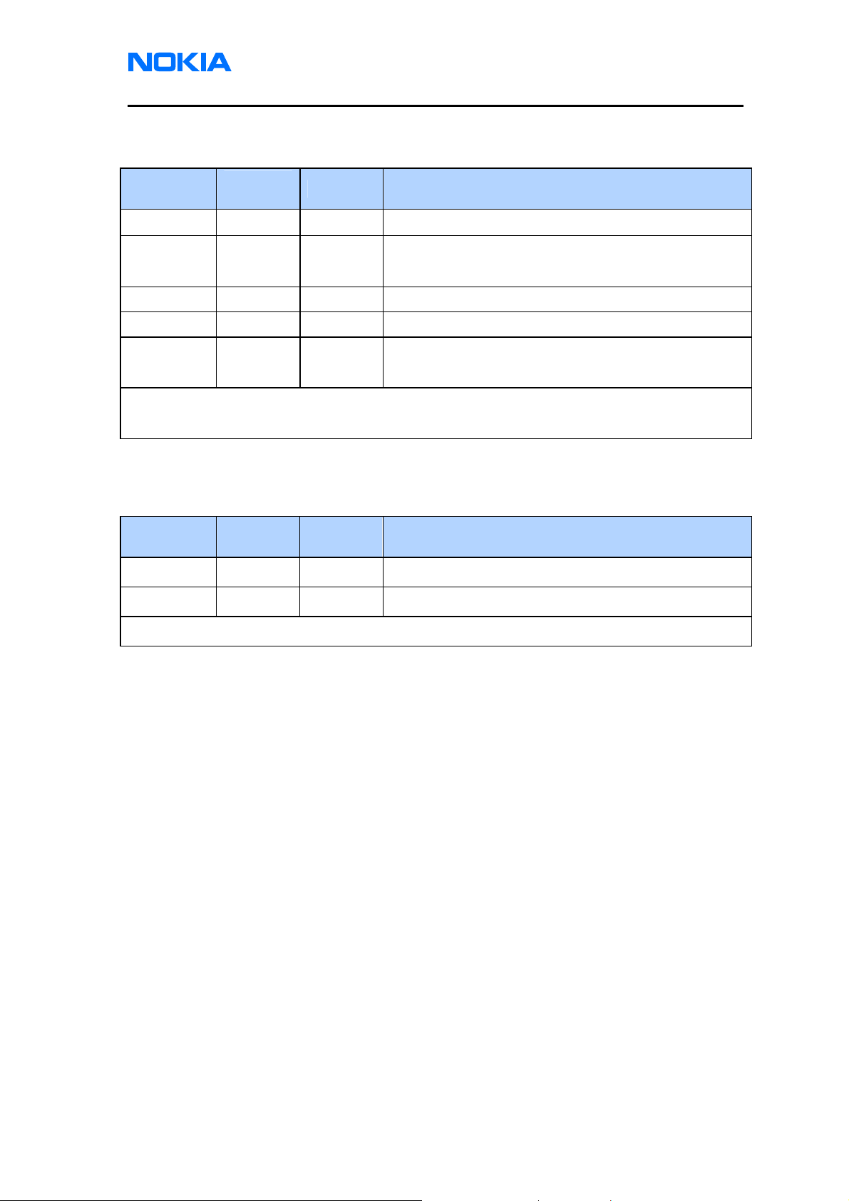
The baseband is powered by the following PM regulators:
Regulator
MSMC 500 mA 1.2 V Always enabled except during power-off mode
MSMA 150 mA 2.60 V
MSMP 300 mA 2.60 V Always enabled except during power-off mode
RUIM 150 mA 3.00 V Enabled only when RUIM card is used
TCXO 50 mA 2.85 V
Note: All output regulators voltage accuracy +/-2%
Table 2 includes the PM regulators for the RF.
Regulator
RFRX 150 mA 2.60 V Enabled when the receiver is on
Rating
Current
Rating
Current
Voltage Notes
Enabled only when the system is powered on (Off
during sleep and power-off modes)
Enabled only when the system is powered on (Off
during sleep and power-off modes)
Table 1: Baseband Regulators
Voltage Notes
RFTX 150 mA 2.60 V Enabled when the transmitter is on
Note: All output regulators voltage accuracy +/-2%
Table 2: RF Regulators
Clock Distribution
The QSC6010 derives its internal clock from two clock inputs, TCXO and
SLEEP_CLK.
The main clock signal for the baseband generates from TCXO
(Temperature-compensated crystal oscillator). The QSC6010’s TCXO clock input
supports the frequency 19.2 MHz +/-2ppm. The SLEEP_CLK provides a 32.768 kHz
+/-20ppm clock source to drive the MSM controller into sleep mode. At this mode,
most of the MSM is powered down and the TCXO is disabled.
Issue 1 04/2007 © 2007 Nokia Corporation Company Confidential Page 9
Page 10
2505 (RM-307)
Baseband Description and Troubleshooting
System Clocks
The PM includes several clock circuits (Figure 4), whose outputs are used for
general housekeeping, MSM and RF functions within the mobile terminal system.
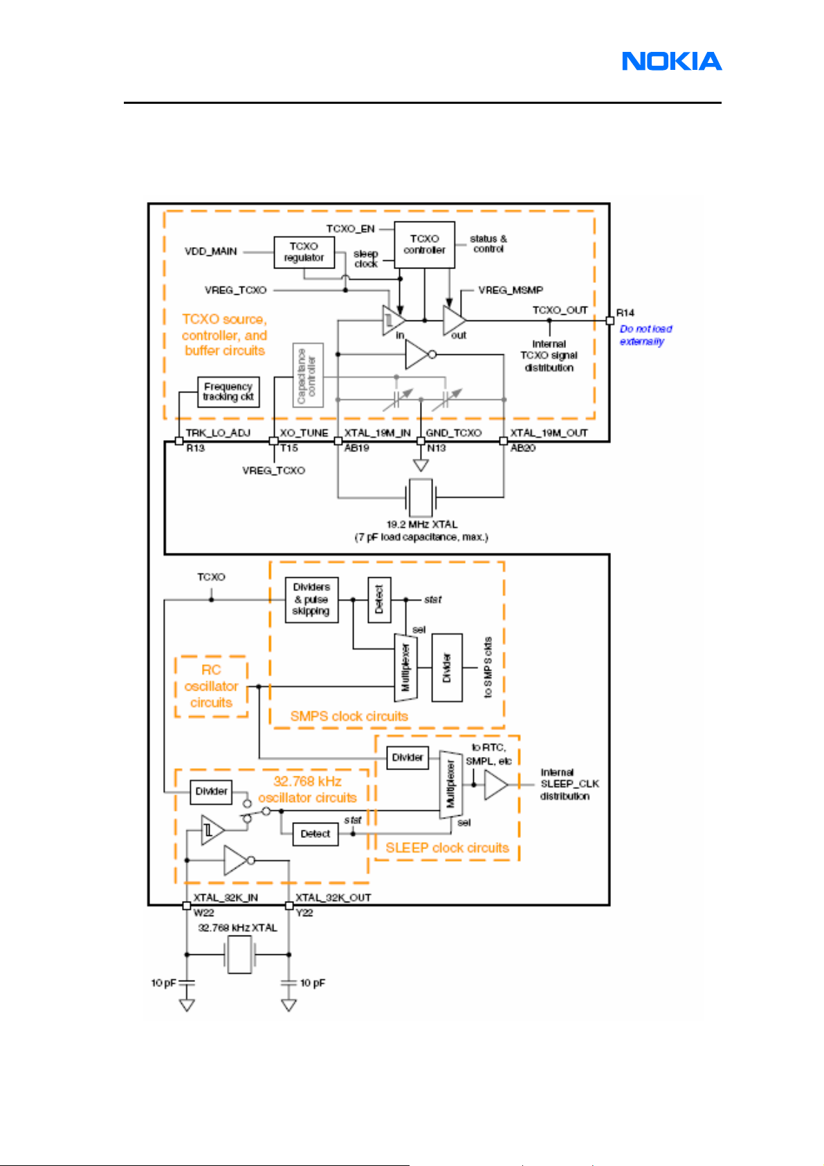
Figure 4: TCXO & SLEEP_XTAL Block Diagram
Page 10 © 2007 Nokia Corporation Company Confidential Issue 1 04/2007
Page 11
2505 (RM-307)
Nokia Customer Care Baseband Description and Troubleshooting
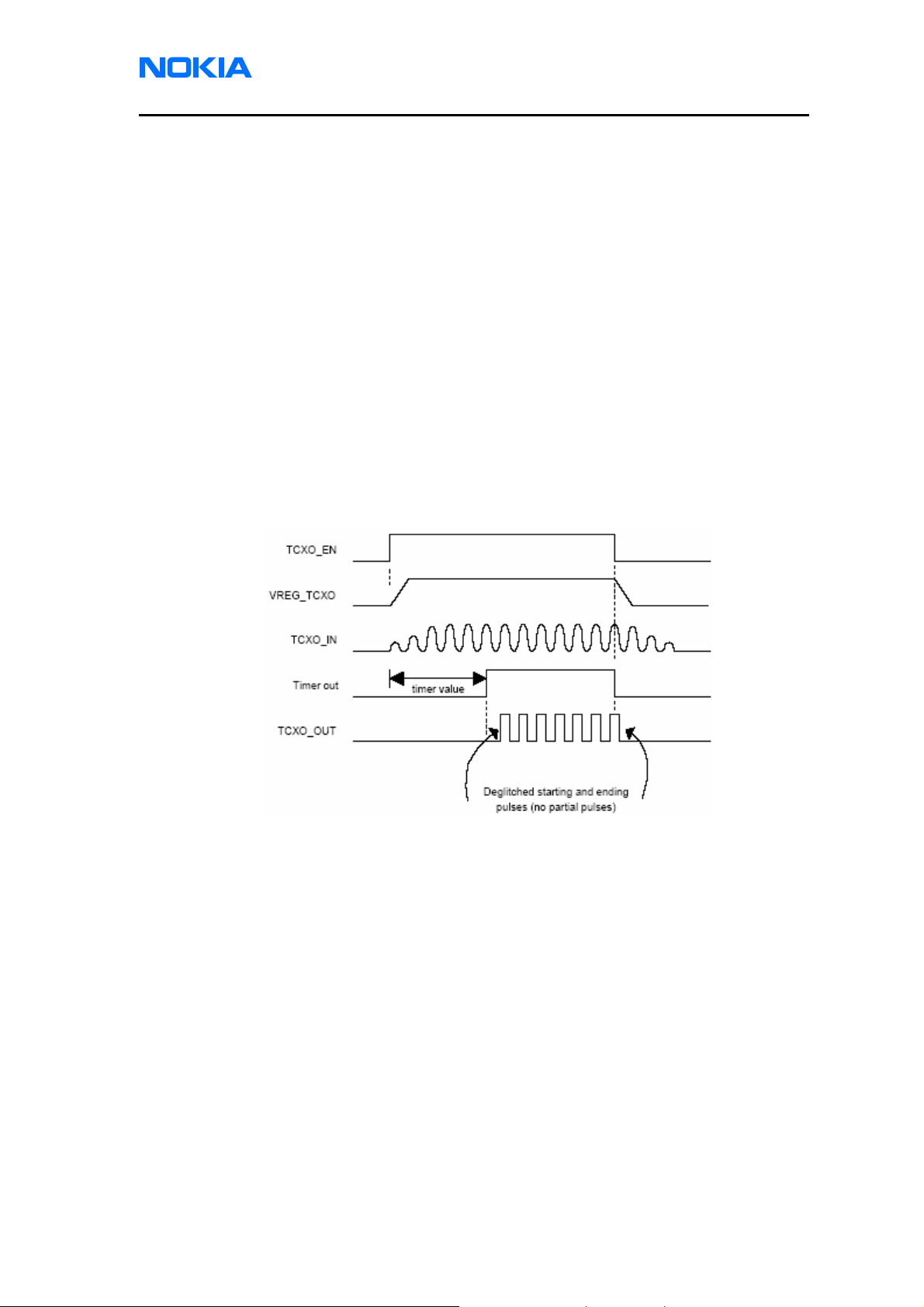
TCXO
The MSM device integrates a phase-locked loop from the TCXO clock input.
The PM optimizes TCXO operation that enables and disables appropriate circuits in
the proper sequence. The controller is enabled by the signal from the MSM.
When the selected transition occurs at TCXO_EN, the controller quickly enables the
TCXO regulator and the input buffer, and begins counting SLEEP_CLK pulses.
Within an initial power on period, the TCXO will be stabilized to its own calibrated
frequency. This initial period, in units of 32.768 kHz clock pulses, is programmed into
a timer within the controller. When the timer expires, the output buffer is enabled. It
synchronizes with the TCXO input such that the TCXO_OUT signal is glitch free,
only valid TCXO pulses are output.
Figure 5: TCXO Enable Timing Diagram
The input buffer (TCXO_IN) accepts sinusoidal or square wave signals at or near
19.2 MHz. The input buffer (TCXO_IN) is powered from the TCXO regulator while
the output buffer is powered by VREG_MSMP.
The regulator of TCXO is turned off after the TCXO_EN signal is removed. Upon
power-up, the PM defaults to this SBI-controlled mode with the TCXO defaulted on.
This assures the MSM will always have a clock available immediately at power-up
even if TCXO_EN is low.
TCXO waveform (19.2MHz +/-2ppm)
Issue 1 04/2007 © 2007 Nokia Corporation Company Confidential Page 11
Page 12

2505 (RM-307)
Baseband Description and Troubleshooting
0
Figure 6: TCXO Timing at 25
P
P
C
SLEEP Crystal Circuit for 32.768 kHz
The 32.768 kHz crystal oscillator is the primary SLEEP clock source when TCXO
clocks are disabled to save power.
Figure 7: Sleep CLK Block Diagram
Page 12 © 2007 Nokia Corporation Company Confidential Issue 1 04/2007
Page 13

2505 (RM-307)
Nokia Customer Care Baseband Description and Troubleshooting
The 32.768 kHz crystal oscillator signal is generated by an external crystal (plus two
shunt capacitors), which is supplemented by a PM internal inverter and buffer.
The crystal oscillator continues to run as long as a valid supply is present, even
when the PM is powered down. This provides a continuous and accurate 32.768 kHz
source. The oscillator halts when power from the external supply and main battery
are removed.
The PM includes a circuit that continually monitors the crystal oscillator signal. If the
crystal stops oscillating, the PM automatically switches to the RC oscillator and
sends an MSM interrupt. Narrow pulses at the SLEEP_CLK output may occur during
this switchover. The crystal oscillator dissipates little power, adjusting its bias current
to the minimum required to maintain oscillation.
SLEEP Clock waveform (32.768KHz +/-20ppm)
0
Figure 8: Sleep_CLK Timing at 25P
P
C
Issue 1 04/2007 © 2007 Nokia Corporation Company Confidential Page 13
Page 14

2505 (RM-307)
Baseband Description and Troubleshooting
SBI CLK Interface
A 9.6 MHz clock signal is used for DBUS, which is used by the MSM to transfer data
between the PM and MSM.
0
Figure 9: MSM to PM SBI Timing at 25P
P
C
The system clock is stopped during sleep mode by disabling the VREG_TCXO.
The TCXO is turned off by the PM regulator, which is from MSM’s TCXO_EN output
signal.
Flash Programming Error Description
This table describes the errors condition during Flash memory downloading to the
mobile terminal.
Description Not Working Properly
Packet Checksum fail ERR: CRC invalid
Erase fail Unable to erase device
Write fail Write unsuccessfully
Figure 10: Flash Programming Error Description
Page 14 © 2007 Nokia Corporation Company Confidential Issue 1 04/2007
Page 15

2505 (RM-307)
Nokia Customer Care Baseband Description and Troubleshooting
Charging Operation
Battery
The 2505 uses a Lithium-Ion cell battery with a capacity of 700 mAh. QSC6010
reads the resistor inside the battery pack on the BSI line to identify the battery size.
Different charging algorithm will be used for different battery sizes. The resistors are
connected to the BSI pin inside the battery connector.
Figure 11: BL-4B battery pack pin order
Charging Circuitry
The PM charge control is dependent on the charger type and the battery size.
External components are needed for electromagnetic compatibility (EMC), and
transient protection of the input to the baseband module. The charger’s DC input is
through the dc-jack connector. This mobile terminal supports AC-3/AC-4 & DC-4
chargers.
Figure 12: Charging Circuitry
Issue 1 04/2007 © 2007 Nokia Corporation Company Confidential Page 15
Page 16

2505 (RM-307)
Baseband Description and Troubleshooting
Charger Detection
Connecting a charger creates a voltage on the VCHG (“VEXT_DC” pin in 2505
schematic) input of the PM. Charging starts when the PM detects the VCHG input
voltage level above 3.3V (Min. working voltage of VCHG pin).
The VCHG signal of PM is generated to indicate the presence of the charger for the
software. The power management (PM) software controls the charger identification/
acceptance. The charger recognition is initiated when the EM software receives
a ”charger connected” interrupt. The algorithm basically consists of the following
three steps:
1. Check that the system current (the collector current of PNP transistor) is within
safety limits.
2. Check the power consumption of PNP transistor is within safety limits.
3. Check that the charger is within the charger window (voltage and current). If the
charger is accepted and identified, the appropriate charging algorithm will be
initiated.
Figure 13: Mobile terminal DC Jack Circuit.
Figure 14: PNP Charging Control Circuit.
Page 16 © 2007 Nokia Corporation Company Confidential Issue 1 04/2007
Page 17

2505 (RM-307)
Nokia Customer Care Baseband Description and Troubleshooting
Charge Control
In active mode, charging is controlled by the PM’s digital part. Charging voltage and
current monitoring are used to limit charging into a safe area. The PM has a
MaxPower protection limit at NPN transistor to cut-off charger.
Cut Off MaxPower = 1000mW
The PM limits the charging voltage to MaxVoltage.
MaxVoltage= 4.25V
The PM limits the total system current (the collector current of PNP transistor) by
limiting the maximum power of NPN transistor charge.
Audio
The audio control and processing is provided by the MSM which contains the audio
codec, the MCU and DSP blocks. These blocks handle and process the audio data
signals. The baseband supports 2 microphone inputs and three receiver (earpiece)/
speaker outputs.
MIC+ & MIC- inputs of 2505 schematic are used for the mobile terminal's internal
microphone. JACK_MIC+ & JACK_MIC- input are used for headsets.
Every microphone input can have either a differential or single-ended AC connection
to the QSC6010 circuit. The internal microphone (MIC+) and external headset
microphone (JACK_MIC) are both differential signals which come from different
sources and are connected to separate inputs at the QSC6010.
The MICBIAS output is used for MIC to provide 1 mA of current at 1.8 +/-0.11Volts
DC.
VDD_MSMP (2.8V) regulated voltage from PM is used for JACK_MIC (external
headset).
RECEIVER+ & RECEIVER- (of QSC6010 output pins) outputs are used for the
mobile terminal's internal receiver (earpiece).
The receiver and external louder speaker are both differential signals that come from
separate outputs at the QSC6010 are connected to different driver.
Issue 1 04/2007 © 2007 Nokia Corporation Company Confidential Page 17
Page 18

2505 (RM-307)
Baseband Description and Troubleshooting
The output power for the differential (RECEIVER) output is typically 35 mW for a
full-scale +3 dBm0 sine wave into a 32 ohm receiver.
The output power for the single-ended (MICROPHONE) output is typically 8.8 mW
for a full-scale +3 dBm0 sine wave into a 32 ohm receiver (earpiece).
The output power for the auxiliary (SPEAKER) output is typically 0.5 mW for a
full-scale +3 dBm0 sine wave into a 600 OHM load.
The 2505 also supports a hands-free speaker.
Display and Keyboard
The mobile terminal uses light-emitting diodes (LEDs) for liquid crystal display (LCD)
and keypad illumination. There is only one white LED for the LCD and the keypad.
VPH_PWR is the signal used to drive this LED driver for the LCD and keyboard.
The mobile terminal uses a color LCD. The interface uses a parallel bus to transfer
the Command/ Data between QSC6010 and LCD.
The panel for 2505 is a 96x65dot matrix FSTN LCD module. It has a FSTN panel
composed of 96 segments and 65 commons. The LCD interface uses parallel bus for
controlled Command/ Data .
Accessories
The 2505 supports the following accessories.
Figure 15: Pop-port bottom connector pin out
The pin out on the 2505 connector is as follows:
• DC Charger Input Æ Blue
• Headset Jack Input Æ Green
You can perform the following in 2505 accessories:
• Charging
• Audio interface headset microphone and receiver (earpiece)
Page 18 © 2007 Nokia Corporation Company Confidential Issue 1 04/2007
Page 19

2505 (RM-307)
Nokia Customer Care Baseband Description and Troubleshooting
Charging
This mobile terminal supports AC-3/AC-4 & DC-4 chargers and be connected
through this interface.
Headset Detection
The mobile terminal supports Nokia standard 2.5mm mono headset. The headset
insertion to the mobile terminal is detected through pin 4 (HS_DET) of the headset
Jack, J580. HS_DET (“JACK_SENSE” pin in 2505 schematic) is low when headset
not inserted. It becomes high when headset is inserted.
Figure 16: Headset Detection Circuit
RUIM CARD
This mobile terminal supports RUIM Card function. Figure 17 shows the timing of
the RUIM’s serial interface.
Figure 17: RUIM Card Serial Timing
Issue 1 04/2007 © 2007 Nokia Corporation Company Confidential Page 19
Page 20

2505 (RM-307)
Baseband Description and Troubleshooting
Test Points – Top
VPH_PWR
AUDIO_OUT_P
AUDIO_OUT_N
VIB_DRV_N VPH_PWR
HPH_L
USB_D+
USB_D-
USB_VBS
PHONE_ON MSM_UART1_TX
MSM_UART1_RXD
VEXT_DC
JACK_MIC+
VPH_PWR
Page 20 © 2007 Nokia Corporation Company Confidential Issue 1 04/2007
Page 21

2505 (RM-307)
Nokia Customer Care Baseband Description and Troubleshooting
ROM_CS_N PA_ ON
GPI053 PA _VMO D
BATT_ID
BATT_ID
CAM_FLASH
VREG_MSMC_S
MIC-
Issue 1 04/2007
BATT_ID
MIC+
© 2007 Nokia Corporation Company Confidential Page 21
Page 22

2505 (RM-307)
Baseband Description and Troubleshooting
Troubleshooting
First, carry out a through visual check of the module. Make sure in particular
that:
• There is no mechanical damage.
• Soldered joints are OK.
• ASIC orientations are OK.
The following hints should help find the cause of the problem when the
circuitry seems to be faulty. Troubleshooting instructions are divided into the
following sections:
• "Mobile Terminal is Dead"
• "Flash Faults"
• "Power Does Not Stay ON or the Mobile Terminal is Jammed"
• "Charger Faults"
• "Audio Faults"
• "Display Faults"
• "Keypad Faults"
Note:
• QSC6010 is underfilled and can not be replaced.
• Memory IC is underfilled and can not be replaced.
• The Shielding Cover can not be reused after removal.
• After using the heat gun, the domesheet needs to be replaced.
Page 22 © 2007 Nokia Corporation Company Confidential Issue 1 04/2007
Page 23

2505 (RM-307)
/
Nokia Customer Care Baseband Description and Troubleshooting
Mobile Terminal is Dead
Mobile
Terminal is
Dead
♦ If current is zero, check L208, Q209, R214
and check the power on sequence. If there is
no power output, Reheat solder joints or
change
Is the mobile
terminal current is
zero or too high?
NO
YES
♦ Make sure all BB regulators are at their respective
voltage levels (VREG_MSMA, VREG_MSMP,
VREG_MSMC, VREG_TCXO). Reheat solder
joints / change if necessary.
Is the current
< 60 mA?
YES
Check RESIN_N
signals. Is it high
(2.8V)?
YES
Check PS_HOLD
signals. Is it high
(2.9V)?
NO
NO
NO
YES
Check the “BSI” line at
J202, C225, R224.
Are they OK?
YES
Reheat solder joints
or change QSC6010
Is flash
programming OK?
YES
NO
NO
Reheat solder joints
change
MSM is defective,
phone can not be
repaired and must
be replaced.
Flash
Faults
Mobile
Terminal is
Jammed
Check ROM_CS_N
(TP56). Is it toggling
after RESIN_N goes
high?
NO
YES
Memory IC is
defective, phone can
not be repaired and
must be replaced.
MSM is defective, phone
can not be repaired and
must be replaced.
Issue 1 04/2007 kia Corporation Compa
© 2007 No ny Confidential Page 23
Page 24

2505 (RM-307)
Y
Y
Baseband Description and Troubleshooting
Flash Faults
Flash
Faults
Measure 19.2MHz
RF CLK at testpoint.
YES
Can the mobile
terminal connect to
PC via UART?
YES
Check ROM_CS_N
(TP56) and WR_N
(R453). Are they
toggling during
programming?
NO
NO
NO
Measure the
19.2MHz CLK
coming from the
ES
MSM is defective, phone can
not be repaired and must be
replaced.
Memory IC is
defective, phone can
not be repaired and
must be replaced.
Is it work?
ES
END
MSM is defective,
phone can not be
repaired and must
be replaced.
NO
Check/ change
VREG_TCXO, Y104
Mobile
NO
Terminal is
Jammed
YES
Memory IC is
defective, phone can
not be repaired and
must be replaced.
Page 24 © 2007 Nokia Corporation Company Confidential Issue 1 04/2007
Page 25

2505 (RM-307)
Y
C
Y
g
Y
g
Nokia Customer Care Baseband Description and Troubleshooting
Power Does Not Stay ON or the Mobile Terminal is Jammed
Mobile
Terminal
Measure VREG_MSMP,
VREG_MSMC,
VREG_MSMA, and
VREG_TCXO voltages.
Are they OK?
YES
Measure 32kHz Sleep
CLK , Is it OK?
YES
Check VPH_PWR, VREG_MSMP,
NO
VREG_MSMC, VREG_MSMA,
and VREG_TCXO capacitors.
Are they OK?
YES
Check “BSI” line
and VPH_PWR line.
ES
NO
Measure the 32 kHz
ES
Reheat solder joints or
e QSC6010
chan
NO
NO
NO
solder joints/ change
TCXO and QSC6010
Reheat solder
Repair capacitors, reheat
joints or
change
QSC6010
hange Y103
Measure 19.2MHz
RF CLK. Is it OK?
YES
Measure RESIN_N.
Is it high (2.8V)?
YES
NO
NO
MSM is defective,
phone can not be
repaired and must
be replaced.
Issue 1 04/2007 © 2007
Measure the
19.2MHz CLK
coming from the
ES
MSM is defective,
phone can not be
repaired and must
be replaced.
Reheat solder joints
or chan
e QSC6010
Nokia Corporation Compa
NO
Check/ reheat solder
joints/ change
VREG_TCXO, Y104
ny Confidential Page 25
Page 26

2505 (RM-307)
r
A
Baseband Description and Troubleshooting
Charger Faults
Charge
Faults
Connect the charger
and make sure the
battery is
connected.
Check the “BSI” line.
Is it about 75k Ohm or
81k Ohm?
YES
Measure voltage
at D205.
Is it >4.5V?
YES
Read MOBILE
TERMINAL_THERM
value. Is it room
temperature?
YES YES
Check/ changeJ202,
NO
C225, R224.
Check/ change DC Jack,
NO
NO NO
L208, D205, C206, R212,
C210 and Q209.
Check RT228 and
R227.
re they OK?
MSM is defective, phone
can not be repaired and
must be replaced.
Replace NTC
or R227
Measure voltage
between pin#1 and pin#3
NO
Change QSC6010
of Q209. Is it >0.7V
YES
Change Q209
Page 26 © 2007
Nokia Corporation Compan Co
y nfidential Issue 1 04/2007
Page 27

2505 (RM-307)
Nokia Customer Care Baseband Description and Troubleshooting
Audio Faults
Audio
Faults 1
Is the onboard
receiver working?
YES
Replace the
NO
receiver
(earpiece). Is it
working now?
NO
Use CCS Service
Software
Audio/Vibra
Æ
TestingÆStereo
Æ
ReceiverÆ Mobile
terminal Receiver Loop Back
Test command
Is the signal coming out of the MSM
on RECEIVER+ and RECEIVER- ?
YES
YES
Retest
Change the
receiver
(earpiece).
NO
Audio
Faults
Page 2
Check/ change C509, C510,
c545. If OK, MSM is
defective, phone can not be
repaired and must be
replaced.
Issue 1 04/2007 © 2007 Nokia Corporation Company Confidential Page 27
Page 28

2505 (RM-307)
g
/
Baseband Description and Troubleshooting
Audio
Faults 2
Is onboard
microphone
working?
YES
Replace the
NO
microphone. Is it
workin
now?
NO
Use CCS Software
Æ
Testing
Æ
Stereo Audio/Vibra
Æ
MicrophoneÆMobile terminal
Microphone Test command
Measure MICBIAS voltage from MIC+
pads. Is it 1.6V~ 1.95V?
YES
Is the signal going to the MSM at
MIC1+ and MIC- at C541?
YES
YES
NO
NO
Retest
change
Check
R538,C573. If OK,
MSM is defective,
phone can not be
repaired and must be
replaced.
Check/ change
C571, C572, R542.
If OK, MSM is
defective, phone can
not be repaired and
must be replaced.
Audio
Retest
Faults
Page 3
Page 28 © 2007 Nokia Corporation Company Confidential Issue 1 04/2007
Page 29

2505 (RM-307)
g
Nokia Customer Care Baseband Description and Troubleshooting
Audio
Faults 3
Is the internal
handsfree speaker
(IHF) working?
YES
Select a ring tone and
NO
measure signals at
L577 and L578. Are the
signals OK?
NO
Measure SPK_N.
Is it OK (2.9V+/-2%)?
YES
Use CCS SoftwareÆTesting
Stereo Audio/Vibra
Æ
SpeakerÆMobile terminal
Speaker control Test command
Æ
YES
Chan
e IHF
MSM is defective,
NO
phone can not be
repaired and must
be replaced.
Check/ change C505,C506 ,
If OK, MSM is defective,
NO
phone can not be repaired
and must be replaced.
Audio
Faults
Page 4
Issue 1 04/2007 © 2007 Nokia Corporation Company Confidential Page 29
Page 30

2505 (RM-307)
V
r
Baseband Description and Troubleshooting
Audio
Faults 4
Is the vibrator
working?
YES
Measure
NO NO
voltage on the
PH_PWR
vibrator. Is it OK?
YES
Use CCS SoftwareÆTestingÆ
Stereo Audio / Vibra
Æ
Vibrator Control Test
Command
Æ
vibrator should
work.
SYE
Reheat solder
joints/ change
battery, CR405,
C408
NO
Check
VPH_PWR
line. Is it OK?
YES
END
Measure the
VIB_DRV_N
signal on the
vibrator. Is the
signal OK?
YES
Change the vibrato
NO
Change the
QSC6010,CR405, C409
Page 30 © 2007 Nokia Corporation Company Confidential Issue 1 04/2007
Page 31

2505 (RM-307)
Nokia Customer Care Baseband Description and Troubleshooting
Display Faults
Issue 1 04/2007 © 2007 Nokia Corporation Company Confidential Page 31
Page 32

2505 (RM-307)
Baseband Description and Troubleshooting
Display
Faults
Page2
Does the display start?
YES
NO
Check U430 pin signals, are
they OK?
YES
Check LCD supply voltage at
J410 pin6. Is it okay?
YES
Check LCD signals:
LCM_CS_N(J410_pin5),
LCM_OE_N(J410_pin4),
LCM_WE_N(J410_pin3),
LCM_RS(J410_pin2). Are the
signals okay?
NO
NO
NO
Chang any bad
component
NO
Check R455,R456,
R457,R458, are
they ok?
YES
Change QSC6010
Phone can not be
repaired and must
be replaced
Change LCD
Module
END
YES
RESET
Page 32 © 2007 Nokia Corporation Company Confidential Issue 1 04/2007
Page 33

2505 (RM-307)
Nokia Customer Care Baseband Description and Troubleshooting
Keypad Faults
Keypad
Faults
Is the power
key working?
YES
Keypad
Faults
Page 2
Measure voltage at
NO NO
Sw9 PIN2 (2.95V).
Is it high?
YES
Measure voltage at
SW9 when power key
is pressed. Is it Low?
NO
Change QSC6010
YES
Change QSC6010
Retest
Issue 1 04/2007 © 2007 Nokia Corporation Company Confidential Page 33
Page 34

2505 (RM-307)
Baseband Description and Troubleshooting
Keypad
Faults
Page 2
Are the UI module
keys working?
NO
YES
END
Measure KEYSENSE(0~4)_N
signals between QSC6010
and keypad at every outer
dome key. Are they 2.9V
+/-0.1V?
YES
Measure
KYPD_(9,11,15,13,17)
signals between
QSC6010 and keypad on
every inner dome Key.
Are they about 0V?
YES
QSC6010 is
defective, phone
can not be repaired
and must be
replace
NO
NO
Make sure there are no shorts
on KEYSENSE(0~4)_N. If OK,
QSC6010 is defective, phone
cab not be repaired and must
be replaced. Otherwise, remove
Make sure there are no
shorts on
KYPD_(9,11,15,13,17). If OK,
QSC6010 is defective,
phone can not be repaired
and must be replaced.
Otherwise, remove the short
Page 34 © 2007 Nokia Corporation Company Confidential Issue 1 04/2007
 Loading...