

Page 1

Nokia Customer Care
2505 (RM-307)
Mobile Terminal
RF Description and
Troubleshooting
Issue 1 04/2007 Company Confidential © 2007 Nokia Corporation
Page 2

2505 (RM-307)
RF Description and Troubleshooting
Contents Page
Component Layout ................................................................................................... 3
Tx Troubleshooting................................................................................................... 5
Tx System Block Diagram .................................................................................5
Tx Introduction...................................................................................................6
Main Tx Component ..........................................................................................6
FTM Setup for Tx Troubleshooting ....................................................................7
Tx DC Test Points..............................................................................................8
Tx RF Test Points..............................................................................................9
Tx DC Test Points............................................................................................10
Tx Path Troubleshooting ................................................................................. 11
Rx Troubleshooting ................................................................................................ 12
Rx System Block Diagram...............................................................................12
Rx Introduction ................................................................................................13
FTM Setup for Rx Troubleshooting..................................................................13
Cell Receiver Check from RF to DVGA...........................................................14
Receiver DC Test Points .................................................................................15
Receiver RF Test Points .................................................................................16
Rx Path Troubleshooting .................................................................................17
Page 2 © 2007 Nokia Corporation Company Confidential Issue 1 04/2007
Page 3
2505 (RM-307)
Nokia Customer Care RF Description and Troubleshooting
Component Layout
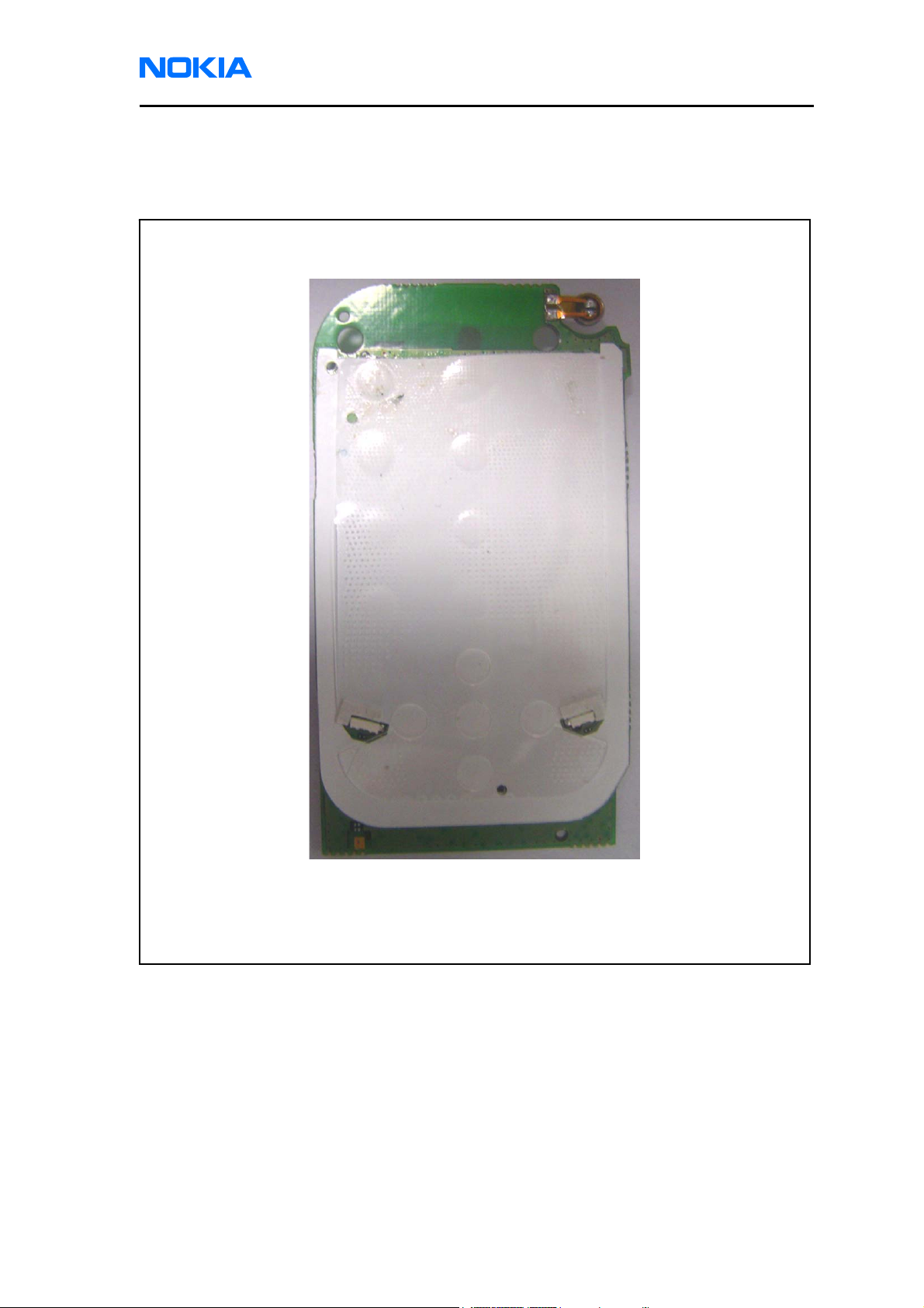
Figure 1 and Figure 2 show the main components of the 2505 mobile terminal.
Figure 1: Component layout (Top)
Issue 1 03/2007 © 2007 Nokia Corporation Company Confidential Page 3
Page 4
2505 (RM-307)
RF Description and Troubleshooting
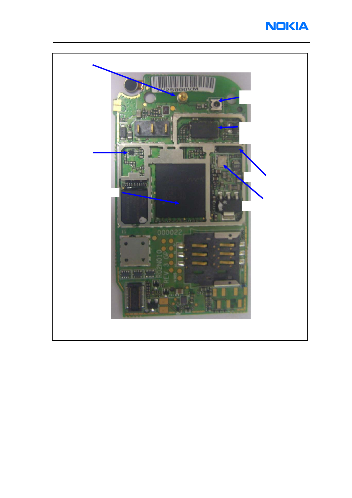
RF Antenna feed point
RF connector
Front end module
(Duplexer/PA/Coupler)
Rx Saw filter
32.768KHz Crystal
QSC6010 single chip
19.2MHz XTAL
Figure 2: Component layout (Bottom)
Page 4 © 2007 Nokia Corporation Company Confidential Issue 1 04/2007
Page 5
2505 (RM-307)
Nokia Customer Care RF Description and Troubleshooting
Tx Troubleshooting
Tx System Block Diagram
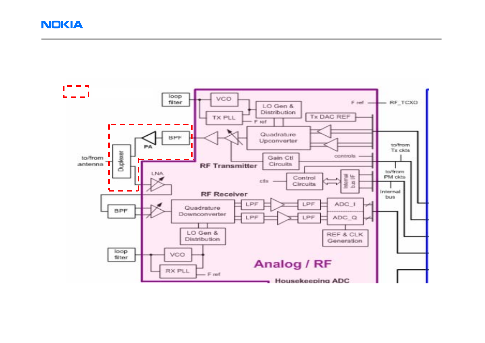
Front End Module
Figure 3: Tx system block diagram
Issue 1 04/2007 © 2007 Nokia Corporation Company Confidential Page 5
Page 6
2505 (RM-3
RF Description and
07)
Troubleshooting
Tx Introduction
The QSC6010 (Figure 3) provides the Zero-IF transmit signal path for Cellular-CDMA transmission. For this chipset, Cellular-CDMA refers
to band classes 0 and 3 as defined by the cdma2000 standard, with mobile station transmitters operating between 824 and 925 MHz. The
transmit signal path includes baseband amplifiers, quadrature upconversion, gain control RF amplification, and an output driver amplifier.
The driver amplifier output is routed to the final stages of the transmit chain – power amplifier, direction coupler, duplexer, and antenna.
Main Tx Component
Front End Module
(Duplexer/PA/Coupler)
QSC6010 Single chip
Page 6
Figure 4: Tx components
© 2007 Nokia Corporation Company Confidential Issue 1 04/2007
Page 7

2505 (RH-104)
Nokia Customer Care RF Description and Troubleshooting
FTM Setup for Tx Troubleshooting
Put PWB on the module jig. Use the following steps to configure FTM for RF
troubleshooting.
1. Connect RF test connector to a spectrum.
2. Set to “FTM mode” in Module Jig.
3. Connect the mobile terminal to a PC via the Module Jig, and connect a
power supply.
4. Open CCS RF Tools software.
5. The FTM dialog box appears.
6. Set “Connect Phone”.
7. Set “Set FTM”.
8. Set “Set Band” to “CDMA800”.
9. Set “Set Channel “to Channel “384”.
10. Set “Set Pa Range R1” to “on”
11. Set “Set TX waveform” to “CDMA”
12. Set “Set TX on/off” to “on”.
13. Set “Set TX AGC” to “90”.
14. Select “ADC Channel” to Channel “4”.
15. Click “Get ADC” bottom to Power detector ADC value.
Figure 5: FTM dialog box
Issue 1 04/2007 © 2007 Nokia Corporation Company Confidential Page 7
Page 8

2505 (RM-307)
RF Description and Troubleshooting
Tx DC Test Points
3
5
2
4
1
Figure 6: Tx DC test point
Table 1 shows the Tx DC test points shown in Figure 6.
Test Point Description Value
1 PA_ON 2.6V for PA turning on, 0V for turning off
2 PA_VMODE 0V for high gain mode 2.6V for low gain mode
3 VREG_MSMP 2.9V
4 VREG_RFTX 2.6V
5 HDET_CELL
Cell: _ 0.37 < 5 dBm _ 0.5 at 15 dBm _ 0.8 V at 25
dBm
Table 1: Tx DC Test Points
Page 8 © 2007 Nokia Corporation Company Confidential Issue 1 04/2007
Page 9

2505 (RH-104)
Nokia Customer Care RF Description and Troubleshooting
Tx RF Test Points
4
3
1
2
Figure 7: Tx RF Test Points
Table 2 shows the test points shown in Figure 7.
Test Point Description Value
1 U6010 output 4dBm
2 PA input 2dBm
3 PA output 28dBm
4 RF connector 24dBm
Table 2: Tx RF Test Points
Issue 1 04/2007 © 2007 Nokia Corporation Company Confidential Page 9
Page 10

2505 (RM-307)
RF Description and Troubleshooting
Tx DC Test Points
5
7 8
6
1
3
2
4
Figure 8: Bottom side Tx DC test points
Table 3 shows the Tx DC test points shown in Figure 8.
Test
Point
Description Value RF Supply Lines Resistance to Ground
1 VREG_MSMP,c250 2.6V >320kΩ to ground U6010
2 VPH_PWR,r214
3 VREG_MSMC,c244
4 VREG_MSMA,c265
5 VEXT_DC,L208
6 VREG_TCXO,L732
7 VREG_RFRX,c278
8 VREG_RFTX,c252
3.2~4.2V >500kΩ to ground U6010,U700
1.2V >9.6kΩ to ground U6010
2.6V >23kΩ to ground U6010
3.2~5.7V ~9.2kΩ to ground Q209
2.85V ~26kΩ to ground U6010,U700
2.6V >320kΩ to ground U6010
2.6V ~1.3kΩ to ground U6010
Table 3: Tx DC Test Points and RF Supply Line Resistance to Ground
*Note: Always measure resistance measure resistance with the phone powered off
Page 10 © 2007 Nokia Corporation Company Confidential Issue 1 04/2007
Page 11

2505 (RM-307)
Y
j
j
Y
Y
Y
Nokia Customer Care RF Description and Troubleshooting
Tx Path Troubleshooting
Tx path
Faults
Measure DC test
points at Table 1. Is it
OK?
YES
NO
Check U6010,U700
NO
Reheat solder joints of U6010
Measure Tx RF test
at Table 3. Is it OK
points 6
YES
NO
Rehear solder
oints of L732,
C714
Measure Tx RF test
points 1
at Table 2. Is it OK
NO
Change U6010
ES
Measure Tx RF test
at Table 2. Is it OK
points 2
ES
NO
Reheat solder joints of L223, U6010
Measure Tx RF test
points 3
at Table 2. Is it OK
ES
Reheat solder
NO
oints of U6010
NO
Change U6010
Measure Tx RF test
points 4
at Table 2. Is it OK
ES
Reheat solder joints of U6010
NO
If RF Antenna feed point pad obstructed,
clean the pad. Connect System Simulator
to MS antenna. Is it OK
Note:
• QSC6010 is underfilled and can not be replaced.
• Memory IC is underfilled and can not be replaced.
• The Shielding Cover can not be reused after removal.
• After using the heatgun, the domesheet needs to be replaced.
Check Antenna Module
NO
Issue 1 04/2007 © 2007 Nokia Corporation Company Confidential Page 11
Page 12

2505 (RM-3
RF Description and
07)
Troubleshooting
Rx Troubleshooting
Rx System Block Diagram
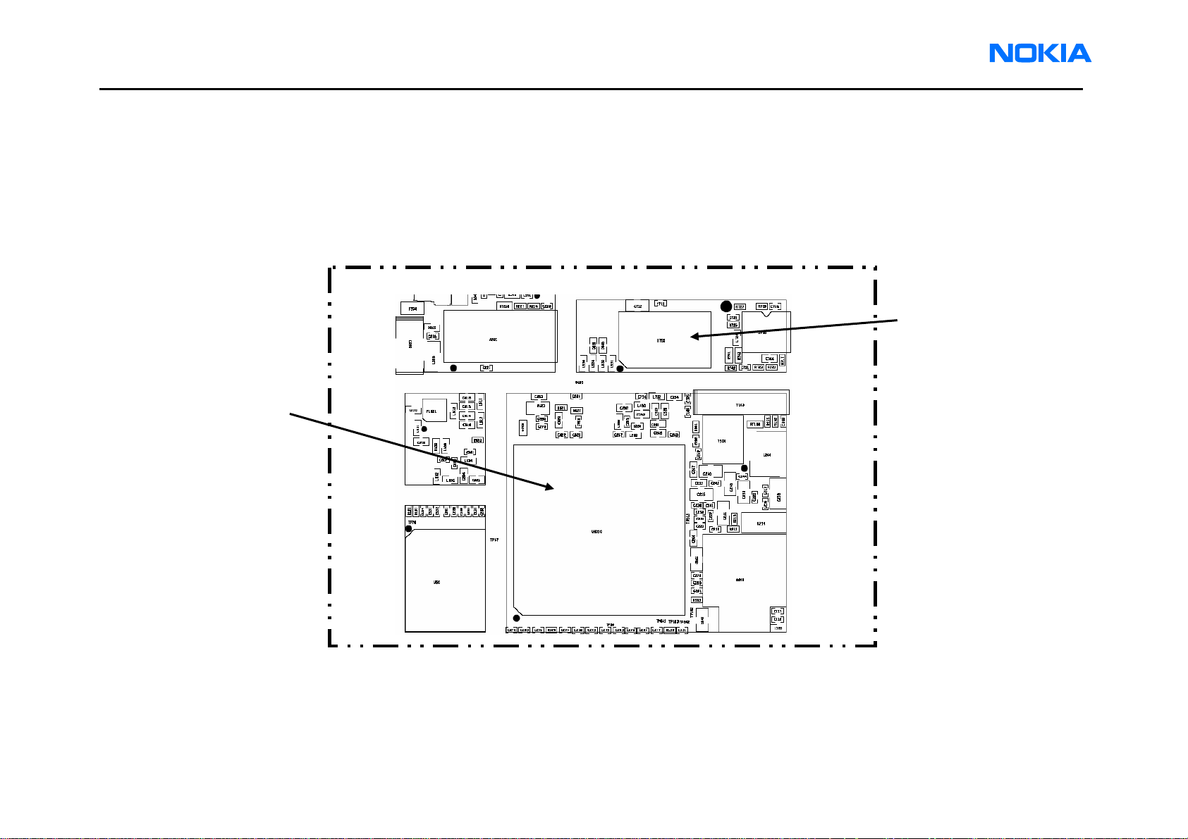
Front End Module
Page 12
Figure 9: Rx DC troubleshooting test points
© 2007 Nokia Corporation Company Confidential Issue 1 04/2007
Page 13

2505 (RM-307)
Nokia Customer Care RF Description and Troubleshooting
Rx Introduction
The QSC6010 IC (Figure 9) provides the Zero-IF receiver signal path for
Cellular-CDMA reception. For this chipset, Cellular-CDMA refers to band classes
0 and 3 as defined by the cdma2000 standard, with mobile station receivers
operating between 832 and 894 MHz. The Rx signal path includes the LNA,
quadrature downconversion, and baseband functions.
The Cellular-CDMA receive signal is routed from the antenna to the QSC6010 IC
via the duplexer. The analog baseband outputs interface with one of Qualcomm’s
Mobile Station QSC6010 devices that also provide status and control signaling.
Integrated Rx LO circuits, ideally supplemented by the QSC6010 transmitter IC,
provide frequency plan flexibility and further reduce PCB parts count.
FTM Setup for Rx Troubleshooting
Put PWB on the module jig. Use the following steps to configure FTM for RF
troubleshooting.
1. Connect RF test connector to a spectrum.
2. Set to “FTM mode” in Module Jig.
3. Connect the mobile terminal to a PC via the Module Jig, and connect a
power supply.
4. Open CCS Service Software and run RF Tools function.
5. The FTM dialog box appears.
6. Set “Connect Phone”.
7. Set “Set FTM “.
8. Set “RF Mode” to “CDMA800”.
9. Set “Set Channel “to Channel “384”.
10. Set “Set LNA Range” to whatever needed.
Figure 10: FTM dialog box
Issue 1 04/2007 © 2007 Nokia Corporation Company Confidential Page 13
Page 14

2505 (RM-307)
RF Description and Troubleshooting
Cell Receiver Check from RF to DVGA
Use the following values to check the CDMA Cell Rx functionality from RF to IQ
output.
1. Start FTM in Local Mode with only the Rx path turned on and set
LNA_GAIN_STATE=0.
2. Inject a –75 dBm CW signal of 881.52 MHz.
3. Get DVGA value from FTM dialog box. The value should approximate 2200.
Page 14 © 2007 Nokia Corporation Company Confidential Issue 1 04/2007
Page 15

2505 (RM-307)
Nokia Customer Care RF Description and Troubleshooting
Receiver DC Test Points
2
1
Figure 11 Rx DC troubleshooting test points
Table 4 includes the descriptions and values for Rx DC troubleshooting test points
shown in Figure 11.
Test Point Description Value
1 VREG_MSMP,c250 2.6V
2 VREG_RFRX,c278 2.6V
Table 4: Rx DC Test Points
Issue 1 04/2007 © 2007 Nokia Corporation Company Confidential Page 15
Page 16

2505 (RM-307)
RF Description and Troubleshooting
Receiver RF Test Points
For the test points in Figure 12, an external signal source of –25 dBm was injected
to the RF input. Set LNA GAIN STATE = 3 .The signal was then traced throughout
the receiver chains. An CMU200 call box is recommended. (Open non-signaling
mode, press the SG soft button, and then select CW.) Inject a continuous wave
(CW) for Cell (881.52MHz) at a fixed –25 dBm power level. Measurements were
taken with the RF Probe. Signal levels are approximate, and the accuracy may be
+/- 2 dB or more depending on the probe position and grounding.
1
3
2
Figure 12 Receiver RF troubleshooting test points
Table 5 includes the descriptions and values for Rx RF troubleshooting test points
shown in Figure 14.
Test Point Description Value
1 LNA IN -28dBm
2 RX SAW INPUT -48dBm
3 RX SAW OUTPUT -51dBm
Table 5: Rx RF Test Points
Page 16 © 2007 Nokia Corporation Company Confidential Issue 1 04/2007
Page 17

2505 (RM-307)
Y
Y
Nokia Customer Care RF Description and Troubleshooting
Rx Path Troubleshooting
Rx path
Faults
Measure DC test
points at Table 4. Is it
OK?
YES
NO
Reheat solder joints of
Check U6010
NO
U6010
Measure Rx RF test
points 1
at Table 5. Is it OK
Reheat solder joints of
NO
L605, C603
YES
Measure Rx RF test
points 2
at Table 5. Is it OK
ES
Reheat solder joints of
NO
C612, L611 and U6010
NO
Change U6010
Measure Rx RF test
points 3
at Table 5. Is it OK
ES
Reheat solder joints of
NO
FL601
Connect System Simulator to MS
antenna.
Check Antenna Module
NO
Note:
• QSC6010 is underfilled and can not be replaced.
• Memory IC is underfilled and can not be replaced.
• The Shielding Cover can not be reused after removal.
• After using the heatgun, the domesheet needs to be replaced.
Issue 1 04/20
07
© 2007 Nokia Corporation Company Confidential Page 17
Page 18

2505 (RM-307)
RF Description and Troubleshooting
This page intentionally left blank.
Page 18 © 2007 Nokia Corporation Company Confidential Issue 1 04/2007
 Loading...