

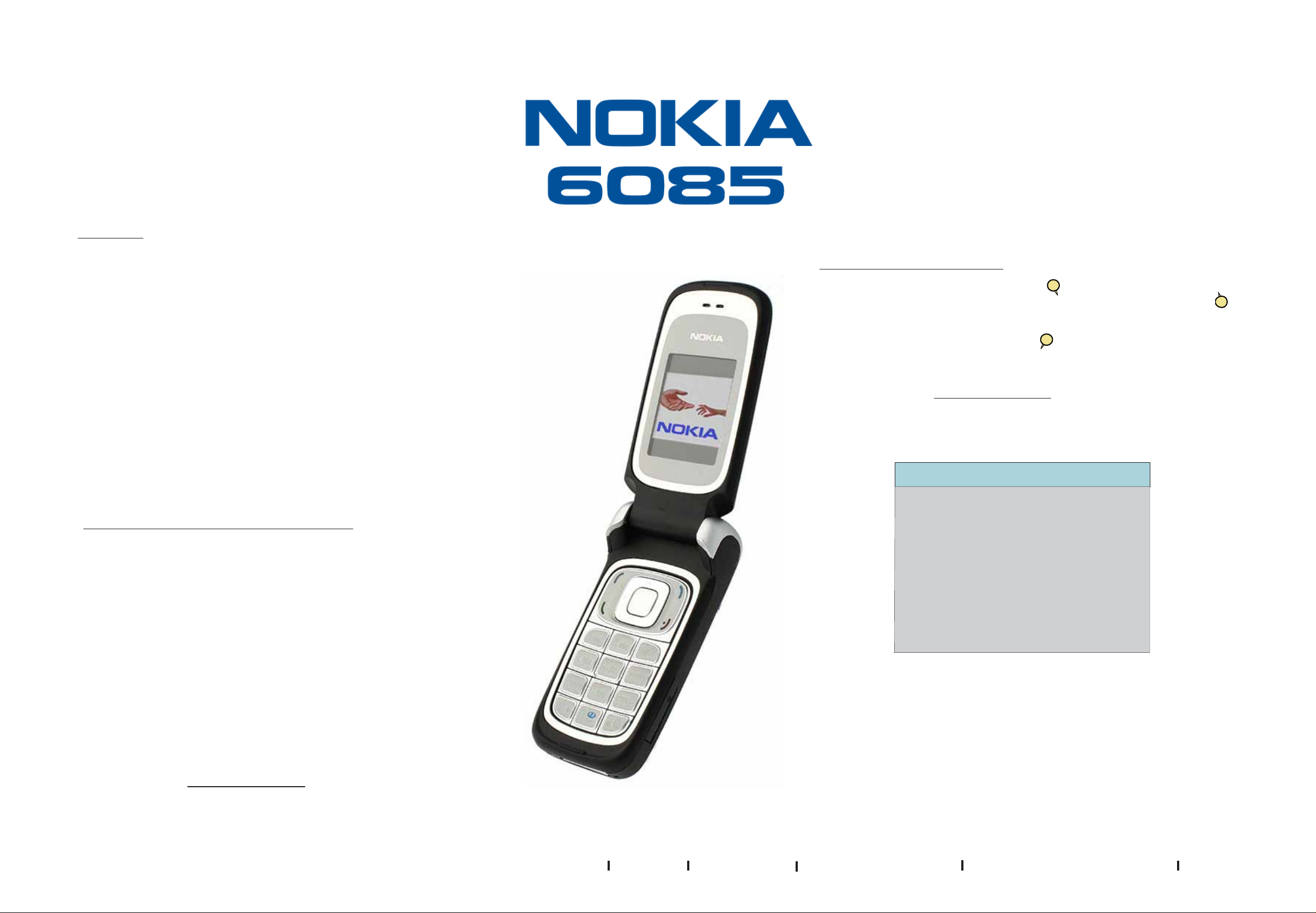
Page 1
Introduction
IMPORTANT:
This document is intended for use by authorized NOKIA servicecenters only.
“Service Schematics”was created with focus on customer care.
The purpose of thisdocument is to providefurther technical repair informationfor
NOKIA mobile phones onLevel 3/4 service activities.
It contains additional information such as e.g. “Componentfinder”.
The “Signal overview” pagegives a good and fast overview about the most
important signals and voltageson board.
Saving process time and improving the repair quality is the aim ofthis document.
It is to beused additionallyto the service manual and other training
or service information such as Service Bulletins.
Service Schematics
RM-198
A NEW FEATURE FOR ON-LINE USE
We have now linked those measurement points which are related to the ocsillograms
shown on the signal overview page. As example: clicking on the measurement point
guides you to the matching oscillogram on the signal overview page. The next click onto
the now shown signal guides you to the related measurement point on the module. Finally,
a third click, now onto the measurement point on the module, takes you back to the
starting point inside the schematics.
Do you have further improvement ideas or would like to give us feedback?
Please send an email to: training.sace@nokia.com
1
1
1
All measurements were made using following equipment:
Nokia repair SW : Phoenix version 2006.34.2.156
Oscilloscope : FlukePM 3380A/B
Spectrum Analyzer : Advantest R3162 with an analog probe
RF-Generator/ GSM Tester : Rhode & Schwarz CMU 200
Multimeter : Fluke73 Series II
While every endeavour hasbeen made to ensurethe accuracyof thisdocument, some
errors may exist. If the reader finds any errors, NOKIA shall benotified in writing.
Please send E-Mail to: training.sace@nokia.com
Table of Content
Front page
System connector
Retu, Tahvo, LED driver
RAPGSM, Memories, FM radio, BT
User interface
Flip PWB
RF part
Signal overview
Component finder
Copyright © NOKIA
This material, including documentationand anyrelated computerprogramsis protected
by copyright, controlledby NOKIA. All rights are reserved. Copying, including reproducing,
modifying, storing, adapting ortranslating any or allof this material requiresthe prior
written consent of NOKIA. This materialalso containscompanyconfidential information,
which may not bedisclosed toothers without the prior written consent of NOKIA.
1
2
3
4
5
6
7
8
9
Customer Care / Training & Vendor Development/ ContentCreationTeam
Confidential - Copyright © 2006 NOKIA Only for training and service purposes
Version: 2.0 05.10.2006 6085/RM-198
Board version: 1VZ_12
Front page
Page 1 (9)
Page 2
Tahvo
Retu
FM radio
CHARGER
XAUDIO(7:0)
FMANT(1:0)
0
1
2
3
4
5
6
7
R2004
10R
HOOKDET
MICB2
MIC2P
XEARL
XEARLC
XEARR
XEARRC
C2007
10n
GND
0
R2005
Charger plug
L2000
220R/100MHz
V2000
L2001
R2006
KA
GND
1
23
B2GND
C2016
470n
GND
C2000
27p
J2002
R2000
220R
C2002
2u2
GND
C2003
33n
C2004
33n
R2003
R2002
10R
C2008
10n
GND
10R
10R
J2003
J2004
C2010
C2009
10n
10n
GND
GND
J2005
J2006
GND
to UEME
R2001
BGF100
1n0
2k2
1n0 1n0
1n0 1n0
2k2
1n0
1k0
50R
50R
1k0
L2004
68nH
Meas
to Mic
GND
GND
GND
GND
GND
Vcc
C2005
C2006
10n
10n
GND
GND
L2002
MCZ1210AD102T
4
L2003
MCZ1210AD102T
4
ESDA18-1F2
MCZ1210AD102T
4
GND
1
23
1
23
ESDA14V2-4BF2
A1
A3
C1
C3
2A
F2000
GND
(phone connected to host)
5V
VBUS
2.5V
(accessory connected)
VOUT
Z2001
600R/100MHz
Z2000
600R/100MHz
11
Z2003
600R/100MHz
C2011
J2000
J2001
GND
charge
charge gnd
ACI
VOUT
Vbus
D+
Ddata gndMIC2N
Xmicn
Xmicp
Xear_l_n
Xear_l_p
Xear_r_n
Xear_r_p
C2013
C2012
10p
10p
C2014
10p
10p
X2002
1
2
System connector
X2000
1
2
3
4
5
6
7
8
9
10
11
12
13
14
GND
AGND
GND
Retu, Tahvo
USB_ACI(7:0)
4
SLAVEPU
1
DPRXD
0
DMTXD
6
MASTPD2
5
MASTPD1
7
ACI
Customer Care / Training & Vendor Development/ ContentCreationTeam
Confidential - Copyright © 2006 NOKIA Only for training and service purposes
R2007
IP4065CX11_LF
2.8V
VAUX
220k
R2008
12
RESNET_220K_120K
GND
120k
34
J2007
J2008
J2009
GND
17k
1k3
33R
33R
15k
GND
Version: 2.0 05.10.2006 6085/RM-198
C2015
220p
R2009
220R
GND
Board version: 1VZ_12
System connector
Page 2 (9)
Page 3
FM radio
RF part
RAPGSM
AUDIO(8:0)
SLOWAD(6:0)
DIG_AUDIO(5:0)
INT_SIM(5:0)
TXC(2:0)
ACI(1:0)
{
CBUS(3:0)
Battery connector
System connector
X2070
VBAT
GND
GND
R2100
EMIF01-SMIC01F2
C2 GND3
1n0
A3
Microphone
B2100
OUT
GND
Power/End key
GND
3.7V
J2071
R2071
14V/50V
VBAT
GND
J2070
BSI
J2072
BGND
CHARGER
S2415
C2074
C2071
10p
27p
GND
GND
2.5V
(accessory connected)
(phone connected to host)
5V
R2403
4k7
1
0
R2070
BTEMP NTC
+
GND
47k
C2073
150u/10V
GND
GND
C2412
-t
0
1
220R/100MHz
C2231
10U
C2307
2u2
GND1
B3
1n0
C3
50R
to Mic
B2
GND2
GND
27p
VREF_INT
R2200
100k
C2072
0
2
1
GND
GND
VOUT
VBUS
C2203
C2202
27p
1n0
0
1
2
3
4
5
220R/100MHz
C2232
1u0
GND
L2202
GND
L2306
600R/100MHz
1.4V
1.8V
C2228
1n0
GND
1u0
GND
GND
VCORE
VIO
GND
0
2
1
L2205
GND
C2306
1u0
C2304
10n
2k2 2k2
2k2
14
to Asic
1n0
GND3
50R
Vbias
150p1n0
C2205
1n0 1n0
GND
C2208
27p
GND
J2200
C2230
1u0
1
2
0
C2309
22u
GND
C2313
1u0
GND
C2206
GND
B1
C1
A2
2.5V1.35V
R2201
120k
C2207
GND
B2200
32.768kHz
23
0
1
2
C2225
L2301
220R/100MHz
R2307
MA21D34001JN
V2302
C2312
1u0
GND
33n
C2100
C2101
33n
R2101
C2102
220R
2u2
GND
5
7
2.5V
C6190
C6191
100n
100n
VANA
4k7
C2209
22p
C2223
R2214
4k7
1n0
1
GND
R2216
2M2
G2200
GND
J2210
J2212
VANA
R2213
C2204
1n0
GND
GND
24
9810
C2281
1u0
GND
C2226
C2227
1u0
1u0
GND
100R
1u0
GND
GND
C2300
C2310
10n
10u
GND
GND
C2302
22u
GND
R2300
4
CURRENT_SEN
BGND
GND
GND
C2224
10n
10n
GND
GND
+
-
GND
J2206
J2300
GND
L2302
10uH
E12
M12
F10
C2233
10u
GND
GND
J2204
J2205
M10
J2207
J2209
G10
C12
K11
K10
C2301
22u
GND
23
1
GND
GND
Retu
D2200
RETU_3.02
HFSpP
HFSpN
HookDet
XEarLC
XEarRC
MicBCap
VSARx
VSATx
MicSub
VDRAM
VSIM2
VRCP1
VRCP2
FlyHigh
FlyLow
VSIM1
SIMDaC1
SIMClkC1
SIMRstC1
SIMDetX
SIMClkC2
SIMDaC2
SIMRstC2
VibraP
VibraN
RetuInt
HeadDet
SleepX
EarP
EarN
Mic2N
Mic2P
XEarL
XEarR
MicB2
VRef
VAna
VAux
VRFC
TxC1
TxC2
Gnd1
Gnd2
Gnd3
Gnd4
GndCP
GndH
MBus
PURX
SlClk
RstX
VBG
VIO
VR1
VCP
AFC
TM
K1
Mic1P
J3
Mic1N
H1
MicB1
E1
Mic3P
E2
Mic3N
E3
Mic3PR
D2
Mic3NR
C3
VDARx
K2
VDATx
PwrOnX
BSI
L3
BTemp
M2
LS
L2
LST
M1
RFTemp
VChar
M3
WTxDet
L9
CrI
K9
CrO
L8
VBack
B6
SIMClk2
A6
SIMDa2
B7
SIMIOC2
J11
WDDis
M4
AudClk
A4
EarDaL
B4
EarDaR
B5
MicData
A3
PMARP
C4
PMARN
C5
SIMClk1
C6
SIMDa1
A5
SIMIOC1
M6
TxCClk
L7
TxCCtrl
L6
TxCDa
HV
L4
MBusTx
K4
MBusRx
M5
SerClk
L5
SerData
K5
SerSelX
VBat6
VBat1
VBat2
A8
VBat3
H12
VBat4
F12
VBat5
B12
VBatCP
B3
VBatH
ChSwS
Tahvo
N2300
TAHVO_V5.2_LF
J1
ChSwS
C1
CbusData
B1
CbusSelX
B2
D9
A7
A6
B5
A4
F10
G10
F9
G9
D10
E10
E9
A5
B6
B4
H10
K10
A3
A10
B10
A8
C10
B8
H2
G2
H3
H4
H5
H6
H7
H8
G3
G8
F3
F8
CbusClk
VCharADC
VBAT1
VBAT1
GND1
GND1
VCharOut1
VCharOut2
VCharOutK
VBAT3
VCharIn1
VCharIn2
VCharInK
VCoreCoil
VCoreCoil
VCore
Vout
VCC
VIO
NC
NC
NC
NC
NC
SENSESENSE+
NC
NC
NC
NC
NC
NC
NC
NC
NC
NC
Slave_PU
Master_PD1
Master_PD2
D+_RXD
D-_TXD
VPP_VIO
RSTX
PURX
SLEEPX
SMPSClk
SleepClk
Clk600
VCCint
TahvoInt
GND3
GND4
GND5
PWM300
GenOut1
GenOut2
GenOut3
VcoreDef
FlashM
TestMode
TestOut
RCV_FRX2
VP_FRX
VM_CLK
SLAVESWSET
CLK
RXD2
OEX
FSE0
VO
FTX
NC
NC
NC
NC
NC
NC
NC
NC
NC
NC
0
D3
D1
1
B1
C2
4
3
L12
2
6
0
J2
J1
F3
F1
G1
G3
H2
R2212
G2
C2200
470R
1u0
C1
H3
F2
H10
C2201
1u0
F11
J12
E11
M11
D12
G11
G12
C9
A10
C10
B10
C2210
B11
A12
1u0
M8
K7
M7
A7
C8
C7
C11
L1
B9
A9
D10
A2
A1
L10
GND
D11
GND
K12
GND
B8
GND
K6
GND
A11
GND
B2
GND
J2208
K8
1.8V
H11
L11
E10
J2216
K3
J2217
M9
J10
2
1.8V: active
0V: sleep mode
J10
H9
J9
J6
K7
J7
K8
A1
B3
12
D2
D1
J2308
E1
E2
F1
C2303
K9
GND
1u0
C2
J8
GND
F2
GND
A9
GND
G1
J2
K1
H1
C9
A2
B7
B9
J4
K4
J5
K2
J3
K3
K5
K6
E3
E8
D3
D8
C3
C4
C5
C6
C7
C8
GND
R2301
3k3
GND
GND
J2309
J2314
J2310
J2311
J2312
J2313
J2315
7
15
GND
GND
GND
GND
GND
C2211
4u7
GND
1.8/3V
3.7V
J2218
J2219
5
4
3
2
1
0
6
7
0
1
2
L2212
220R/100MHz
L2211
220R/100MHz
0
1
2
3
2
0
3
5
1
7
0
1
2
VRCP2
GND
13
4.7V
C2221
1u0
0
1
VRCP1
GND
C2212
1u5
GND
L2270
220R/100MHz
L2271
220R/100MHz
}
C2222
1u0
C2274
Traceability pad
X2060
C2220
1u5
GND
C2275
GND
1
GND
PWMTAHVO
27p27p
C2270
1n0
C2271
1n0
GND
1.8V
VRFC
VR1
C2213
C2214
1u5
1u5
GND
GND
EMIF03-SIM02F2
C2273
1n0
C2103
C2104
GND
Flash interface
RXD2
RXD
CLK
TXD
LED driver
N2301
TPS61061YZFR
A2
EN
C2
SW
B3
FB
A3
ILED
GND
C2105
C2272
27p
1n0
1.8V2.5V
VIO
C2215
1u5
GND
R2700
R1
R2
R3
10p10p
J2060
4
GND
678
123
OUT
VIN
GND
PGND
VPP
VBUS
C1
B1
A1
C3
GND
1.8V
SIM Reader
L2304
22uH
GND
L2100
56nH
C2106
27p
2.8V
VDRAM
C2219
1u5
GND
Side
A2102
66
55
1QD
44
3
PWB VIBRA LIFTING
3
7
4
5
6
3
2
1
0
600R/100MHz
C2315
C2314
4u7
GND
L2101
56nH
2.5V
VAUX
VANA
C2217
C2216
1u5
1u5
GND
GND
C2700
GND
100n
GND GND
GND
10
9
Vibra
8
7
L2305
C2305
1u0
C2317
27p
4u7
GND
GND
AUDIO(8:0)
A2100
1
3
4
IHF speaker
2
GND
1.35V
VREF_INT
VREF
SIM connector
X2701
470191501
1
2
3
PUSL(7:0)
3.7V
VBAT
GND
7V
(illumination active)
X2400
XAUDIO(7:0)
System connector
}
TXC_CONV(2:0)
5
6
7
USB_ACI(7:0)
System connector
RAPGSM, BT, FM radio
EMINT(1:0)
{
VLEDOUT1
Flip connector,
keyboard illumination
SETCURR1
INTUSB(8:0)
RF part
RAPGSM
GEN_OUT(3:0)
RAPGSM
UI
Customer Care / Training & Vendor Development/ ContentCreationTeam
Confidential - Copyright © 2006 NOKIA Only for training and service purposes
Version: 2.0 05.10.2006 6085/RM-198
Board version: 1VZ_12
Retu, Tahvo, LED driver
Page 3 (9)
Page 4

Retu, Tahvo
RF part
TXC(2:0)
Retu
ACI(1:0)
{
DIG_AUDIO(5:0)
INTUSB(8:0)
Tahvo
INT_SIM(5:0)
Retu
Camera
via X2400
Retu, Tahvo
C2828
C2824 C2823
100n
PUSL(7:0)
RFCLK(1:0)
RFCTRL(8:0)
{
RFCONV(11:0)
CCP_CMT(3:0)
EMINT(1:0)
C2829
100n
27p
C2819
100n 100n
C2830
100n
RAPGSM
D2800
RAPGSM_V1.1PA
J8
GND
TMAct
GENIO0
3
1
0
0
C2825
1n0
5
6
GND
0
1
0
4
5
1
2
6
7
8
3
R2806
68k
GND
0
1
2
3
5
7
464
0
1
2
2
R2803
100R
19
3
0
R2804
18
100R
1
1.4V
VCORE
C2803
C2806
C2816
100n
100n
100n
1.8V
VIO
C2812
C2820
GND
100n
100n
GND
C2814
C2813
100n
100n
100n100n
1.8V
0
1
2
3
4
5
6
7
9
8
0
1
L2409
33R/100MHZ
L2408
33R/100MHZ
L2407
33R/100MHZ
L2406
33R/100MHZ
100n
C2833
100n
VRFC
25
RXRESET
31
1
2
0
0
1
2
3
1
5
0
6
2
3
4
5
6
0
1
C2807
5082C2282C
1u0
R3002
10R
C2800
100n
C2831C2826
C2801
27p
C2809
C2808
100n
100n
GND
C2
C1
D3
R11
R8
4
J2851
F3
F2
M3
N1
N8
26
N3
N7
J2833
N4
N2
J2834
M8
P3
K4
K3
L3
L4
J2828
H2
J2829
H3
J2830
J3
J2831
J4
J2
K7
GND
L7
A19
A20
D17
D16
B18
W8
1
2
Y8
3
Y9
0
R10
4
W9
5
V9
Y2
W3
V4
W2
U4
V3
U2
PUEN
V2
D18
C20
E18
B19
C18
C17
B17
D2
E4
F4
E3
E2
J7
A7
B7
C7
D7
C6
H8
B5
C5
D6
B4
C4
D5
A3
B3
D4
A2
C3
H13
W10
Y14
Y18
P20
GND
D20
B16
G3
E21
A17
AA13
AA17
R21
AA9
B1
G2
M4
W1
AA5
Y21
L21
H15
A13
A9
A5
H20
H7
K8
H4
M7
Y1
GND
Y6
Y10
P15
M20
J21
B21
B14
B10
B6
GND
M2
AA1
AA11
AA21
M14
100n
N21
G21
A21
A11
A1
E1
J1
L8
G4
GND
G1
GND
L1
GND
K2
GND
GND
SleepX
SleepClk
PURX
SMPSClk
SysClk
RFClkP
RFClkN
TXReset
TXP
TXA
RX1
RX2
RFBusClk
RFBusDa
RFBusEn1X
GENIO52
TxIP
TxIN
TXQP
TXQN
RxIP
RxIN
RxQP
RxQN
VrefP
VrefN
Iref1
TxCDa
TxCDaCtrl
TxCClk
ACIRx
ACITx
EarDataL
EarDataR
MicData
AudioClk
PMARP
PMARN
USBVP_FRX
USBVM_Clk
USBRCV_FRX2
USBVO
USBFSE0_FTX
USBOEX
GENIO71
USBDSyncClk
SIMClk1
SIMIOCtrl1
SIMIODa1
SpeciallO0
SpeciallO1
SpeciallO2
SpeciallO3
JTClk
JTrst
JTDI
JTMS
JTDO
EMU0
ETMClk
ETMPkt0
ETMPkt1
ETMPkt2
ETMPkt3
ETMPkt4
ETMPkt5
ETMPkt6
ETMPkt7
ETMSync
ETMPipe0
ETMPipe1
ETMPipe2
ETMSyncB
ETMPipeB0
ETMPipeB1
ETMPipeB2
RetuInt
TahvoInt
VSSDSP1
VSSDSP2
VSSDSP3
VSSMCU1
VSSMCU2
VDDDPÖÖ
VDDMCU1
VDDMCU2
VDDDSP1
VDDDSP2
VDDDSP3
VDDDSP4
VDDCORE1
VDDCORE2
VDDCORE3
VDDCORE4
VDDCORE5
VDDCORE6
VDDCORE7
VDDCORE8
VDDCORE9
VDDCORE10
VDDCORE11
VDDDLLDCDL
VSSCORE1
VSSCORE2
VSSCORE3
VSSCORE4
VSSCORE5
VSSCORE6
VSSCORE7
VSSCORE8
VSSCORE9
VSSCORE10
VSSCORE11
VSSCORE12
VSSCORE13
VSSCORE14
VDDSIO1
VDDSIO2
VDDSIO3
VDDSIO4
VDDSIO5
VDDSIO6
VDDSIO7
VDDSIO8
VDDSIO9
VDDSIO10
VDDA
VDDARX
VDDATX
VSSA
VSSARX
VSSATX
VSSASUB
GENIO1
GENIO2
GENIO3
GENIO4
GENIO5
GENIO6
GENIO7
GENIO8
GENIO9
GENIO10
GENIO11
GENIO12
GENIO13
GENIO14
GENIO15
GENIO16
GENIO17
GENIO18
GENIO19
GENIO20
GENIO21
GENIO22
GENIO23
GENIO24
GENIO25
GENIO26
GENIO27
GENIO28
GENIO29
GENIO30
GENIO31
GENIO32
GENIO33
GENIO34
GENIO35
GENIO36
GENIO37
GENIO38
GENIO39
GENIO40
GENIO41
GENIO42
GENIO43
GENIO44
GENIO45
GENIO46
GENIO47
GENIO48
GENIO49
GENIO50
GENIO51
GENIO53
GENIO54
GENIO55
GENIO56
GENIO57
GENIO58
GENIO59
GENIO60
GENIO61
GENIO62
GENIO63
GENIO64
GENIO67
GENIO68
GENIO69
GENIO70
GENIO72
GENIO73
CBusClk
CBusDa
CBusEn1X
I2SSCLK
I2SWS
I2SSD1
I2SSD2
APESleepX
SDRAd0
SDRAd1
SDRAd2
SDRAd3
SDRAd4
SDRAd5
SDRAd6
SDRAd7
SDRAd8
SDRAd9
SDRAd10
SDRAd11
SDRAd12
SDRAd13
SDRAd14
SDRCLK
SDRCKE
SDRRASX
SDRCASX
SDRWEX
SDRDQML
SDRDQMU
SDRCLKX
SDRLDQS
SDRUDQS
ExtAdDa0
ExtAdDa1
ExtAdDa2
ExtAdDa3
ExtAdDa4
ExtAdDa5
ExtAdDa6
ExtAdDa7
ExtAdDa8
ExtAdDa9
ExtAdDa10
ExtAdDa11
ExtAdDa12
ExtAdDa13
ExtAdDa14
ExtAdDa15
ExtAdDa16
ExtAdDa17
ExtAdDa18
ExtAdDa19
ExtAdDa20
ExtAdDa21
ExtAdDa22
ExtAdDa23
ExtAdDa24
FlsADVX
FlsRSTX
FlsWEX
FlsOEX
FlsCSX
FlsCS2X
FlsWaitX
GENIO66
GENIO65
SDRDa0
SDRDa1
SDRDa2
SDRDa3
SDRDa4
SDRDa5
SDRDa6
SDRDa7
SDRDa8
SDRDa9
SDRDa10
SDRDa11
SDRDa12
SDRDa13
SDRDa14
SDRDa15
AA20
AA19
AA15
FlsClk
0
N15
1
U20
2
U19
3
T18
4
V20
5
U18
6
W21
7
V19
8
W20
9
N14
10
Y20
11
W19
12
V18
13
14
Y19
15
16
W7
17
V7
18
W6
19
R9
20
Y5
21
W5
22
V6
23
Y4
24
V5
25
AA3
26
W4
27
Y3
28
AA2
29
P9
J2803
30
W11
31
J2804
V11
32
V17
33
W18
34
V16
35
W17
36
Y17
37
P14
38
W16
39
Y16
40
V15
41
W15
42
Y15
43
44
R14
45
V14
46
W14
47
R13
48
AA7
49
V8
50
P10
51
Y7
53
G14
54
B20
55
C19
56
P2
57
P4
58
P7
59
R1
60
R2
61
R3
62
R4
63
T2
64
T3
67
V10
68
P11
69
P8
70
U1
U3
72
73
T4
P13
V12
W12
Y13
V13
W13
Y12
B2
E20
F20
N20
C21
K15
T20
M15
L15
J15
T19
R20
L14
K14
J20
G20
K19
U21
H14
K20
J14
J19
L18
K18
D19
R19
B9
B8
C11
C10
D9
D8
H10
G9
C12
D12
D11
D10
C9
C8
H9
G8
G11
A15
C13
B15
C16
G10
B13
H11
H12
C15
D15
D14
C14
B12
D13
G13
G12
P12
R12
F19
G19
G18
H18
F18
H19
E19
J18
L19
R18
M18
P19
N18
P18
M19
N19
WPX
VPPLOCK
0
1
2
3
4
5
6
7
8
9
10
11
12
13
14
15
16
17
18
19
20
21
22
23
24
0
1
2
3
4
5
6
7
9
8
SDRAM_DA(15:0)
0
1
2
0
1
2
3
4
5
6
7
8
9
10
11
12
0
1
2
3
4
5
6
7
8
9
10
11
12
13
14
15
MEMCONT(15:0)
GENIO00
3
GENIO03
7
GENIO07
8
GENIO08
9
GENIO09
11
GENIO11
GENIO12
12
13
GENIO13
46
GENIO46
GENIO16
16
17
GENIO17
18
GENIO18
19
GENIO19
20
GENIO20
GENIO21
21
GENIO22
22
GENIO23
23
24
25
26
28
55
27
30
31
32
33
34
35
36
37
38
39
40
41
68
53
52
48
49
50
51
62
63
72
73
59
60
64
67
69
70
29
44
47
0
1
2
3
0
1
2
3
4
5
6
7
8
9
GENIO24
GENIO25
GENIO26
GENIO5
GENIO28
GENIO55
GENIO27
GENIO30
GENIO31
GENIO32
GENIO33
GENIO34
GENIO35
GENIO36
GENIO37
GENIO38
GENIO39
GENIO40
GENIO41
GENIO68
GENIO53
GENIO52
GENIO48
GENIO49
GENIO50
GENIO51
GENIO62
GENIO63
GENIO72
GENIO73
GENIO59
GENIO60
GENIO64
GENIO67
GENIO69
GENIO70
GENIO29
GENIO44
GENIO47
DIFWRX Gabes/ SDA Rebun
DIF D/Cx Gabes/SCL Rebun
CAM_ENABLE (xshutdown)
BTDAIN
BTDAOUT
BTRSTX
UART_WAKE
BTCTS
BTRTS
BTWAKE
SDRAM_AD(15:0)
SDRAM_BA(1:0)
SDRAM_CTRL(10:0)
1.8V
{
VIO
R3004
4k7
MEMADDA(24:0)
VIO
KEY_light_EN
DIFCSX Gabes
LCDCS2X Rebun
LCD_RESX Gabes
DIFRDX Gabes
1
2
0
6
3
4
5
0
1
R3003
4k7
1.7/9V
LED_SWITCH
ENABLE
DATA
CMD
DATADIR
CMDDIR
CLK
SDCARDDET
MESSI0
MESSI1
MESSI2
MESSI3
MESSI4
MESSI5
MESSI6
MESSI7
SDA
SCL
CAM_CLK
CAM_VCTRL
VPP
Key_EN
20
1
0
14
2
1
7
6
0
15
0
1
2
3
4
5
6
1.8V
7
{
17
VIO
VIO
21
LCDTE
16
185
19
20
1k0
22
R2801
R2802
0
1
17
2
3
4
5
6
8
9
10
0
1
4
SENSOR_INT
FM_INT
J3000
0
1
2
3
4
5
6
7
7
8
9
10
6
11
1
J3001
0
7
2
3
4
0
1
8
8
5
9
9
6
R3000
4k7
GND
J3002
16
17
18
19
20
21
22
23
5
9
5
4
8
J3003
3
J3004
0
7
1
2
J3005
0
1
2
3
4
5
6
7
8
9
10
11
12
13
14
15
0
J3006
1
2
3
4
5
6
7
8
9
10
11
12
13
14
15
UI_CTRL_CMT(4:0)
MESSI_CMT(25:0)
1k0
1
I2C(1:0)
0
16
KEYB_CMT(20:0)
CAM_CTRL_CMT(4:0)
CBUS(3:0)
Retu, Tahvo
Combo memory
D3000
K5G5629ATB-SF75
COMBO 256M NOR +
128M DDR DRAM
P10
0
M10
N10
M3
P4
N4
M4
Ad
P5
N5
M5
M9
N9
11
M6
CKE
DDR
P7
CK
N7
_CK
L3
_CS
P6
A1_index
_RAS
N6
_CAS
M8
_WEd
P9
BA0d
N8
BA1d
C11
LDQS
B9
LDM
B4
UDQS
C6
UDM
J1
16
E3
F3
F2
A
L1
K1
E2
F1
23
NOR
G1
_CEnor
G2
D12
G3
H3
M13
E14
E13
F14
F13
H14
J14
K14
K13
D13
E12
G14
G13
H13
H12
L14
L13
C13
B12
C12
A11
B11
A10
B10
C10
A6
A5
B5
C5
C4
B3
C3
C2
K2
L2
_WP
_OE
_WE
CLK
RDY
_AVD
_RESET
Address/Data I/O
NOR
Data I/O
DDR
VDRAM
VDRAM
VDRAM
VDRAM
VDRAM
VDRAM
VDRAM
VDRAM
UI
UI
Camera
via X2400
UI
}
D1
NC
D2
NC
D3
NC
E1
NC
J3
NC
K3
NC
K12
NC
M1
NC
M2
NC
M11
NC
M12
NC
N11
NC
N12
NC
P3
NC
D4
A1
DNU
A2
DNU
A13
DNU
A14
DNU
B1
DNU
B14
DNU
N1
DNU
N14
DNU
P1
DNU
P2
DNU
P13
DNU
P14
DNU
A4
VIO
B7
VIO
B8
VIO
B13
VIO
N13
VIO
H2
VIO
L12
VIO
G12
VIO
P11
P8
N3
D14
C8
C1
A9
A8
H1
VPP
C3000
A7,B2,C7,C14,M7,N2,P12= GND
GND
C3001
10n
GND
1.7/9V
VPP
C3008
100n
100n
GND
A3,A12,B6,C9= GND
F12,J2,J12,J13,M14= GND
VBAT
C3201
1u0
GND
1.8V
C3005
100n
C3002
100n
GND
C3009
100n
GND GND
VIO
GND
1.8V
VDRAM
2
0
1
6
7
14
C3006
C3003
100n
DATA
CLK
CMD
CARDDET
CMDDIR
DATADIR
ENABLE
C3202
10n
1.8V 2.8V3.7V
10n
GND
GND
R3201
100k
20
VIO
GND15GND
C3007
C3004
100n
1.8V
VIO
R3202
22k
1.8V
J3201
R3206
33R
J3203
GND
VMMC
C3205
C3203
27p
1u0
GND
1.8V: flip open
0V: flip closed
10n
GND
GND
R3205
33R
LP3928TLX-1828_NOPB
B3
Dir1
B2
Dir2
C3
Dir3
A4
EN1
A2
EN2
C2
LatchClk
A1
VBAT
B4
VCCA
B1
VCCB
1.8V
6
4
5
1
2
3
4
0
3
2
1
0
22
VIO
R2402
1
0
2
N3200
100k
C2413
10n
GND
C6157
10n
GND
1.8V
21
J3200
C4
A1
D4
A2
D3
A3
C1
B1
D1
B2
D2
B3
A3
GND
GND
Hinge sensor
N2402
MRUS71D
4
Out1
MR SENSOR
C6158
100n
10k
R6159
100k
R6160
C6170
C6165
1u5
100n
GND
VAUX
2.8V
0R
R2422
R2420
GND
BTH_CLK_REQ
UART_WAKE
UART_CTS_P
BT_WAKEUP
UART_TX
UART_RX
UART_RTS
UART_CTS
BT_RESETX
PCM_OUT
PCM_IN
PCM_SYNC
PCM_CLK
R6030
VIO
10k
R3203
100k
C3204
Avdd23Out2
100k
100n
Gnd
GND
1
R6157
GND
2.8V
VMMC
R3204
2k2
47nH
L6156
C6168
100n
GND
22R
10R
R6156
Bluetooth
E3
PIO0
F4
PIO1
F3
PIO8
G5
NC
G6
NC
G7
NC
D7
PIO6
E5
PIO5
D4
PIO7
F1
PIO9
G1
PIO2
G2
PIO3
E6
PIO4
B5
UART_TX
A5
UART_RX
A7
UART_RTS
A6
UART_CTS
E7
RESETB
D5
PCM_OUT
B7
PCM_IN
C5
PCM_SYNC
B6
PCM_CLK
D2
RF_IN
C7
VSS_DIG
G3
VSS_PADS
B1
VSS_VCO
C1
VSS_RADIO
B3
VSS_ANA
C2
B2
B1
C1
D1
2.8V
VAUX
A1
A2
A3
A4
B2
E1
E2
C2
D6
E4
A6
A5
D1
C6164
100n
GND
N6030
BC4-ROM1.0RDL
EMIF04-MMC02F2
R10
R20
C2402
10n
GND
FM radio
N6156
TEA5760_N1C
CPOUT
LOOPSW
LO1
LO2
INTX
DATA
CLOCK
BUSEN
TMUTE
MPXOUT
VCC
VCCVCO
VDD
AUX_DAC
RF_A
RF_B
XTAL_IN
AIO0
AIO2
VREG_EN
VREG_IN
VDD_ANA
SPI_CSB
SPI_CLK
SPI_MOSI
SPI_MISO
VDD_PIO
VDD_PADS
VDD_CORE
VDD_VCO
VDD_RADIO
TEST_EN
R3200
BUSMODE
VREFDIG
RFIN1
RFIN2
RFGND
SWPORT
TIF_centre
VAFR
AGND
DGND
FREQIN
F2
E2
E1
A3
C4
B4
C3
A2
A4
F6
F5
E4
F7
G4
D6
C6
B2
C2
D3
2.8V
R1
R2
R3
R4
VAFL
3A2A
B3
C3
D3
S3200
GND D2
12
MiniSD hatch
detection switch
C3200
L6176
GND
C6189
100n
120nH
C6178
C6179
100n
27p
47p
GND
GND
1.8V
VIO
D3
E3
B6
C6
C5
B1
D5
E6
E5
C6188
100n
B5
D2
GND
C1
VMMC
600R/100MHz
GND
C6176
100p
L3200
MMCCMD
MMCCLK
MMCGND
MMCDA
GND
0
7
5
1
microSD connector
X3200
1
2
3
4
5
6
7
8
GND
FMANT(1:0)
System connector
AUDIO(8:0)
Retu
}
PUSL(7:0)
BT antenna
Z6302
X6300
4
3
GND
GND
1
RFCLKEXT(1:0)
PUSL(7:0)
RF part
Retu
SLEEPCLK
1
PURX
0
1.8V
100k
R6035
GND
VIO
1.8V
C6033
C6039
L6030
L6031
10n
2n7H
2n7H
C6032
GND
18p
GND
C6051
2p7
LDB182G4505C-110
C6052
2p7
GND
SYSCLK
100p
15
C6034
10n
GND
C6036
10n
GND
GND
T6030
6
4
C6040
C6340
1
6p8
3
C6031
18p
GND
3.7V
VBAT
C6055
1u0
GND
R6032
2R2
C6037
1u0
1u5
GND
GND
OUTIN
6p8
GND
GND
GND
R6034
L6032
10k
R6031
22nH
10k
C6038
10n
GND
C6035
10n
GND
Z6300
2450MHz
C6342
Customer Care / Training & Vendor Development/ ContentCreationTeam
Confidential - Copyright © 2006 NOKIA Only for training and service purposes
Version: 2.0 05.10.2006 6085/RM-198
Board version: 1VZ_12
RAPGSM, Memories,
FM radio, microSD, BT
Page 4 (9)
Page 5

Keyboard
RAPGSM
Tahvo
UI_CTRL_CMT(4:0)
KEYB_CMT(20:0)
MESSI_CMT(25:0)
{
CAM_CTRL_CMT(4:0)
GEN_OUT(3:0)
V2402
V2401
EMH25T2R
3
4
GND
0
1
2
3
4
5
6
7
16
22
20
19
17
18
21
1
0
Kb illumination
CL-480S-WHS-D-TS
CL-480S-WHS-D-TS
V2404
5
4k7
47k
R2409
180R
10
9
3
2
1
6
0
8
5
4
MESSI0
MESSI7
DIFCXS Gabes
DIFRDX Gabes
LCD_RESX Gabes
DIFD/Cx Gabes/SCL Rebun
DIFWRX Gabes/SDA Rebun
LCDCS2X Rebun
LCDTE
0
7V
VLEDOUT1
2
0
LED SWITCH
GND
V2404
EMH25T2R
4k712
V2400
V2403
6
47k
R2411
180R
GND
EMIF10-COM01F2
OUT1
OUT2 IN2
OUT3
OUT4
OUT5
OUT6
OUT7
OUT8
OUT9
OUT10
GND
GND
GND
CL-480S-WHS-D-TS
CL-480S-WHS-D-TS
IN1
IN3
IN4
IN5
IN6
IN7
IN8
IN9
IN10
GND
GND
GND
ROW0
ROW1
ROW2
COL4
COL3
COL2
COL1
COL0
ROW4
ROW3
ROW2
ROW1
ROW0
S2412
S2414
COL2
LEFTSK
SEND
ROW0
ROW3
ROW3
ROW4
ROW1
ROW4
ROW2
ROW4
COL1
COL3
LEFT
S2400
S2403
S2406
S2409
S2419
UP
S2418
S2422
GND
GND
S2421
RIGHT
2
S2402
5
S2405
8
S2408
0
S2411
COL4
COL2
COL3
Z2403
EMIF10-COM01F2
OUT1
OUT2
OUT3
OUT4
OUT5
OUT6
OUT7
OUT8
OUT9
OUT10
GND
GND
GND
Z2404
EMIF10-COM01F2
OUT1
OUT2
OUT3
OUT4
OUT5 IN5
OUT6
OUT7
OUT8
OUT9
OUT10
GND
GND
GND
COL1
COL0
ROW4
ROW2
GND
GND
IN10
GND
GND
IN10
31
6
9
#
IN1
IN2
IN3
IN4
IN5
IN6
IN7
IN8
IN9
IN1
IN2
IN3
IN4
IN6
IN7
IN8
IN9
S2420
DWON
S2401
4
S2404
7
S2407
*
S2410
COL4
RIGHTSK
S2413
COL0
Camera key
S2423
Vol+/up
S2416
GND
GND
Vol-/down
S2417
Retu
RAPGSM
RAPGSM
AUDIO(8:0)
CCP_CMT(3:0)
I2C(1:0)
EARN
MESSI0
MESSI1
MESSI2
MESSI3
MESSI4
MESSI5
MESSI6
MESSI7
DIFCXS Gabes
DIFRDX Gabes
CCP_CLKN
CCP_CLKP
CCP_DataN
CCP_DataP
LED SWITCH
SDA
CAM_CLK
CAM_ENABLE
LCDTE
Flip connector
X2400
1
2
EARP
3
4
5
6
7
8
9
10
11
12
13
14
15
16
17
18
19
20
21
22
23
24
25
26
27
28
29
30
31
32
33
SCL
34
35
36
37
38
39
40
1.8V
VIO
L2401
600R/100MHz
C2406
1u0
GND
7V
VLEDOUT1
SETCURR1
1k0
R2416
39R
R2410
2.8V
VAUX
GND
L2402
600R/100MHz
C2407
1u0
GND
GND
1
0
C2400
1
0
22p
GND
1
0
3
2
C2401
22p
DIFWRX Gabes/SDA Rebun
DIFD/Cx Gabes/SCL Rebun
LCD_RESX Gabes/Rebun
LCDCS2X Rebun
Customer Care / Training & Vendor Development/ ContentCreationTeam
Confidential - Copyright © 2006 NOKIA Only for training and service purposes
Version: 2.0 05.10.2006 6085/RM-198
Board version: 1VZ_12
User interface
Page 5 (9)
Page 6

C1001
C1000
1.8V
4u7
VIO
GND
2.8V
VAUX
4u7
GND
L1010
600R/300mA
L1011
600R/300mA
Flip connector
X1000
1
2
GENIO(16) MESSI0
3
GENIO(17) MESSI1
4
GENIO(18) MESSI2
5
GENIO(19) MESSI3
6
7
EARP
8
EARN
9
GENIO(25) LCDTE
10
11
12
GENIO(53) CAM_ENABLE (xshutdown)
13
GENIO(5) LCDCS2X Rebun
14
GENIO(55) LCD_RESX Gabes / Rebun
15
16
GENIO(68) CAM_CLK
17
GENIO(31) Serial Clk CCI
18
GENIO(30) Serial Data CCI
19
GENIO(3) LED_SWITCH
20
21
VLEDOUT1
22
SETCURR1
23
24
CCP DataP
25
CCP DataN
26
27
CCP CLKP
28
CCP CLKN
29
30
31
GENIO(24) DIFWRX Gabes / SDA Rebun
32
GENIO(27) DIFRDX Gabes
33
34
GENIO(26) DIFCSX Gabes
35
GENIO(28) DIFD/CX Gabes / SCL Rebun
36
GENIO(23) MESSI7
37
GENIO(22) MESSI6
38
GENIO(21) MESSI5
39
GENIO(20) MESSI4
40
GND
Camera connector
X3000
1
VCAP
CAM_CLK
CCISCL
CCISDA
CCPCLKN
CCPCLKP
CCPDataP
2
3
C3000
4
220n
5
6
7
8
9
10
11
12
GND
GND
GND
C3001
C3011
100n
10p
GND
GND
1.8V
VIO
GND
C3010
XSHUTDOWN
CCPDataN
0
1
2
3
2.8V
VAUX
C3002
10p
4u7
GND
GND
Main display
MESSI(0:7)
7
6
5
4
VLEDCUT1
DCX,SUB_SCL
LCD_TE
RESX
MAIN_LED-
X2000
1
2
3
RDX
4
5
6
7
8
9
10
11
12
13
CSX
14
15
16
17
18
19
20
21
22
GND
MESSI1
MESSI3
MESSI5
MESSI7
MESSI6
MESSI4
MESSI2
MESSI0
6
4
2
0
2.8V
VAUX
C2000
4u7
1
3
5
7
C2001
100n
GND
1.8V
VIO
GND
EARP
EARN
SETCURR1
14V/50V
R1600
GND
6
EMH25T2R
V1101
either R1701 or L1700 assembled
R1701
10R
L1700
HAC
4k712
47k
R1601
GND
R1101
22k
MCZ1210AD102T
1
23
14V/50V
L1600
OUT
GND
V1102
DTD723YMT2L
R1
5
4k7
47k
V1101
EMH25T2R
3
4
GND
IN
R2
Sub display
X2100
SUB_CSX
RESX
VLEDCUT1
SUB_LED-
1
2
3
4
5
6
GND
7
8
9
10
C2101
100n
1.8V
VIO
GND
C2100
100n
2.8V
VAUX
GND
DCX,SUB_SCL
C1600
27p
4
Earpiece
B1600
Customer Care / Training & Vendor Development/ ContentCreationTeam
Confidential - Copyright © 2006 NOKIA Only for training and service purposes
Version: 2.0 05.10.2006 6085/RM-198
Board version: 1WJ_09
Flip PWB
Page 6 (9)
Page 7

Antenna pads
J7506
J7507
RF chip
N7505
INP_2150
INN_2150
OUTP_FDD
OUTN_FDD
INP_MIX
INN_MIX
INP_1900
INN_1900
INP_1800
INN_1800
DAC1O1
DAC1O3
DAC2O1
DAC2O3
RFC6
RFC7
RFC9
W_OUTP
W_OUTM
INP_900
INN_900
INP_850
INN_850
GNDVCO
GNDLNA
GNDMIX
GNDPRE_RX
GNDPRE_TX
GNDBB_RX
GNDBB_TX
GNDDIG
GNDVGA
GNDRF_TX
GNDCP
RFC4
G_OUTP
G_OUTM
DAC2O2
DAC1O2
RFC5
RFC8
RFC3
RFC2
RFC1
DET
P_OUTP
P_OUTM
MUX_IN
REFG
THERMAL BALLS=
AHNE401A
VBAT_RX
VBAT_TX
VR3_RX
VR1_TX
VR2_TX
VVCO_EXT
VPRE_RX
VPRE_TX
VRF_TX
VVGA
VDAC
VB_EXT
RBEXT_TX
RBEXT_RX
LO_INN
LO_INP
CPOUT_RX
CPOUT_TX
VCO_IN
OSCIN
C1PQ
C1NQ
C2PQ
C2NQ
RXOUT_PI
RXOUT_NI
RXOUT_PQ
RXOUT_NQ
TXQ_0
TXQ_180
TXI_180
DAC_REF1
VREF_CM
SDATA
XENA
XRESET
REFM
MUX_OUT
GND
VLNA
VMIX
VDIG
C1PI
C1NI
C2PI
C2NI
TXI_0
SCLK
REFP
H2
L12
C7504
J1
L11
M11
L10
C6
C3
K1
K7
F11
C11
M2
VCP
K12
L7
E2
C10
H1
M8
M7
L1
L8
M3
L9
G3
H3
G2
G1
E3
F3
F1
F2
K4
M4
L4
L5
J11
J12
H12
H11
K10
C2
L6
M5
K5
M6
M9
K9
B10
TXC
B3
1u0
R7506
10R
R7507
10R
10k
R7502
C7501
2p7
GND
GND GND GND GND
GND
C7509
10p
GND
GND
C7508
18p
2.8V
VR2_TX
GND
C7506
1u0
C7505
1u0
C7518
100n
C7503
C7502
1u0
10p
C7586
10n
GNDGNDGND
C7514
33n
GND
R7503
4k7
4
RXIP
5
RXIN
6
RXQP
7
RXQN
3
TXQN
2
TXQP
0
TXIP
1
TXIN
1
1
DAC_REF1
VREFCM
RFBUSDAT
RFBUSCLK
RFBUSENA
TXRESETX
RFCLKP
RFCLKN
}
}
}
TXC
RFTEMP
8
9
7
6
8
0
0
1
A2
A3
B1
C1
D1
E1
A4
Z7501
SAWEP1G84CM0F04
UNBAL_IN
UNBAL_IN
UNBAL_IN
UNBAL_IN BAL_OUT
BAL_OUT
BAL_OUT
BAL_OUT
BAL_OUT
GND
1800/1900MHz
GND
Z7504
SAWEP881MCM0F04
BAL_OUT
BAL_OUT
GND
BAL_OUT
GND
850/900MHz
28
850/900MHz
R7510
Out
15R
Z7505
L=
W=0.30
GND
X7505
4
GND
3
GND
3.7V
VBAT
Z7520
28R/100MHz
C7524
1p8
LMSM43AA-341
27
TX_1
18
RX_2
19
RX_1
16
RX_4
17
RX_3
21
ANT
14
Vcc2
23
Vcc1
C7520
3p3
GND
Vc
GND GND
FEM
N7520
RF9282E6.5
GND
Icont_h
Icont_I
Vgain
Vdet
Ident
TX_2
Z7503
Vpd
VC3
VC2
VC1
In_1
In_2
9
28
2
3
4
5
6
7
25
10
L7500
L7501
28
30
12nH
30
8n2H
30
Z7521
2400-2483MHz
GND GND
R7522
27k
INOUT
GND
22nH
L7504
T7520
LDB211G8010C-001
1
2
GND
C7522
1p8
30
3
5
4
GND
C7525
18p
22nH
L7505
VC4
Gen_ctrl
PWRDET_G_ctrl
VC3
VC2
VC1
GND
29
0.2-2.1Vpp dep. on PL
A5
A6
A7
E10
D11
H10
G11
C7
C8
B9
B12
C12
A8
A9
A10
A11
K3
C5
D3
J3
K8
J2
J10
K6
D10
F10
K2
GND
D2
D12
E12
G10
E11
K11
B8
B5
B4
C4
B11
F12
G12
C9
M10
C7510
27p
GND
600R/100MHz
RAPGSM
RFCONV(11:0)
RAPGSM
RFCTRL(8:0)
RAPGSM
RFCLK(1:0)
Retu
TXC_CONV(2:0)
Retu
SLOWAD(6:0)
L7502
EHF2BE3800
3
5
GND
4
GND
T7501
VBAT
3.7V
VRCP1
4.7V
VRCP2
4.7V
38.4MHz
15nH
VCC
ENFVK3W2F07
GND
VCC
G7501
NKG3176D
GND
C7590
100p
L7515
R7508
10R
GND
C7515
4p7
G7500
VCONT
GND
C7507
22k
68k
R7501
2k2
C7516
470p
GND
C7513
10n
R7509
22k
10n
GND
R7590
V7590
BFR93AW
R7591
1k5
R7592
GND
8k2
R7505
C7511
2n2
GND
0
0R
R7593
C7592
100n
GND
1
RFCLKEXT(1:0)
Retu
AFC
TXC_CONV(2:0)
Bluetooth
VR1
2.5V
VREF
1.35V
1
2
27
VCO
OUT
VCTCXO
OUT
3
Customer Care / Training & Vendor Development/ ContentCreationTeam
Confidential - Copyright © 2006 NOKIA Only for training and service purposes
Version: 2.0 05.10.2006 6085/RM-198
Board version: 1VZ_12
RF part
Page 7 (9)
Page 8

C2410 D3 C7525 D8 L2306 M4 R7510 D7
B
B2100 Q1 C2411 D3 C7586 D5 L2401 B3 R7522 D7
B2200 P6 C2412 N6 C7590 K1 L2402 D2 R7590 K1
C2000 N8 C2415 B3 L2407 I8 R7592 K2
C2001 N8 C2416 D2 D2200 O6 L2408 I8 R7593 J1
C2002 R4 C2700 Q3 D2800 H6 L2409 I8
C2003 R4 C2800 H8 D3000 J6 L3200 L2 S2416 F8
C2004 R4 C2801 F7 L6030 H3 S2417 H8
C2005 R3 C2803 H8 F2000 P8 L6031 I3 S2423 K8
C2006 R3 C2805 F7 L6032 I4 S3200 O1
C2007 Q2 C2806 F8 G2200 G4 L6156 R5
C2008 Q3 C2807 I5 G7500 B3 L6176 R6 T6030 H2
C2009 Q3 C2808 G8 G7501 D2 L7500 C5 T7501 C2
C2010 Q3 C2809 G8 L7501 C5 T7520 B7
C2011 R3 C2812 H8 J2000 P8 L7502 D4
C2012 R3 C2813 F5 J2001 Q8 L7503 D7 V2000 O8
C2013 R3 C2814 G8 J2002 P6 L7504 C5 V2302 L4
C2014 R3 C2815 F7 J2003 Q3 L7505 C5 V2400 O6
C2015 Q4 C2816 I5 J2004 Q3 L7515 C3 V2401 I6
C2016 P8 C2819 I5 J2005 R2 V2402 I3
C2071 G3 C2820 F6 J2006 Q2 N2300 M6 V2403 O3
C2072 P2 C2822 F5 J2007 Q4 N2301 M8 V2404 N7
C2073 E5 C2823 I6 J2008 Q4 N2402 D7 V7590 K1
C2074 F2 C2824 J5 J2009 P4 N3200 G3
C2100 Q2 C2825 F7 J2060 P2 N6030 H3 X2000 R4
C2101 Q2 C2826 I7 J2070 E3 N6156 Q5 X2002 R7
C2102 Q2 C2828 I7 J2071 E3 N7505 C4 X2060 B6
C2103 E8 C2829 G8 J2072 E4 N7520 C7 X2070 F3
C2104 E8 C2830 H5 J2200 N4 X2400 C3
C2105 D2 C2831 I7 J2204 P5 R2000 Q4 X2701 P3
C2106 C2 C2833 I6 J2205 P6 R2001 Q4 X3200 M2
C2200 O5 C3000 K5 J2206 M4 R2002 Q3 X6300 G2
C2201 P7 C3001 J5 J2207 N4 R2003 Q3 X7505 C8
C2202 P8 C3002 K5 J2209 M4 R2004 Q2
C2203 P6 C3003 J8 J2210 P6 R2005 Q3 Z2000 Q5
C2204 P6 C3004 J8 J2212 J8 R2006 Q3 Z2001 Q4
C2205 P5 C3005 J8 J2216 N6 R2007 Q4 Z2003 Q5
C2206 P6 C3006 K8 J2217 N4 R2008 Q4 Z2400 D6
C2207 P7 C3007 K8 J2218 M4 R2009 Q4 Z2403 C4
C2208 Q6 C3008 J8 J2219 N4 R2070 P2 Z2404 C2
C2209 Q6 C3009 K8 J2300 N6 R2071 E3 Z6300 H2
C2210 N7 C3200 L2 J2308 N6 R2100 Q2 Z6302 F1
C2211 N7 C3201 G2 J2309 M7 R2101 P2 Z7501 C6
C2212 N6 C3202 G3 J2310 M7 R2102 D2 Z7503 D5
C2213 O7 C3203 H3 J2311 N7 R2103 C2 Z7504 C6
C2214 O7 C3204 L4 J2312 M7 R2200 P8 Z7520 B6
C2215 O7 C3205 G3 J2313 N7 R2201 P7 Z7521 B7
C2216 O7 C6031 I2 J2314 N7 R2212 O5
C2217 P7 C6032 H2 J2315 M7 R2213 P7
C2218 P6 C6033 H4 J2803 G5 R2214 P8
C2219 P7 C6034 H3 J2804 G5 R2216 Q7
C2220 N6 C6035 I4 J2828 F6 R2301 M8
C2221 N8 C6036 H4 J2829 F6 R2307 L4
C2222 N7 C6037 H4 J2830 F6 R2402 D7
C2223 O5 C6038 H4 J2831 F6 R2403 N6
C2224 P5 C6039 H3 J2833 F6 R2404 G1
C2225 P7 C6040 I4 J2834 F6 R2409 N8
C2226 O7 C6051 H3 J2851 F7 R2410 D4
C2227 N6 C6052 I3 J3000 K6 R2411 N7
C2228 O7 C6055 H2 J3001 K6 R2416 B3
C2229 N6 C6056 H4 J3002 I5 R2420 H4
C2230 P7 C6157 Q4 J3003 K6 R2422 G4
C2231 N5 C6158 Q5 J3004 J7 R2700 Q4
C2232 O7 C6164 Q5 J3005 J7 R2801 D3
C2233 G4 C6165 R6 J3006 I7 R2802 D3
C2270 O5 C6168 Q6 J3112 L4 R2803 I8
C2271 O5 C6170 R5 J3113 L3 R2804 H8
C2272 O5 C6176 R6 J3114 L3 R2806 F6
C2273 N6 C6178 R6 J3115 L3 R3000 J5
C2274 N6 C6179 Q6 J3116 L2 R3002 H8
C2275 N5 C6188 Q6 J3117 L2 R3003 I8
C2281 O8 C6189 Q6 J3118 L4 R3004 K7
C2300 M5 C6190 P5 J3119 L4 R3200 L1
C2301 L5 C6191 P5 J3200 G3 R3201 G4
C2302 N5 C6340 I2 J3201 G3 R3202 G3
C2303 L7 C6342 I2 J3203 G3 R3203 K5
C2304 N6 C7501 B4 J7506 A8 R3204 L4
C2305 L8 C7502 D4 J7507 C8 R3205 G3
C2306 M4 C7503 D3 R3206 G4
C2307 L6 C7504 B4 L2000 O8 R6030 H4
C2309 L5 C7505 D3 L2001 Q3 R6031 H4
C2310 L6 C7506 D3 L2002 Q3 R6032 I4
C2312 L6 C7507 D3 L2003 R3 R6034 H3
C2313 L7 C7508 D3 L2004 R3 R6035 H4
C2314 M7 C7509 D3 L2100 D2 R6156 Q4
C2315 N8 C7510 D4 L2101 C2 R6157 R6
C2316 N8 C7511 C3 L2202 P8 R6159 R5
C2317 O8 C7513 D3 L2205 P8 R6160 R4
C2318 L8 C7514 D3 L2211 N5 R7501 C3
C2400 N4 C7515 B3 L2212 N6 R7502 B4
C2401 N4 C7516 C3 L2270 O5 R7503 D4
C2402 D7 C7518 D4 L2271 O5 R7505 C3
C2403 D2 C7520 B7 L2301 L5 R7506 D3
C2404 D2 C7522 D6 L2302 M5 R7507 B4
C2406 C3 C7523 B7 L2304 M7 R7508 D3
C2407 D3 C7524 D6 L2305 L7 R7509 D3
C2413 C7 C7592 J1 L2406 I8 R7591 K1
C
D
F
G
J
L
S
T
V
N
X
R
Z
Top
VCTCXO
Battery connector
microSD connector
VCO
SIM connector
RF chip
BT
System connector
RAPGSM
CMT memories
Tahvo
Retu
FEM
Bottom
RF connector
Flip connector
Volume up
Volume down
Camera key
FM radio
Customer Care / Training & Vendor Development/ ContentCreationTeam
Confidential - Copyright © 2006 NOKIA Only for training and service purposes
Version: 2.0 05.10.2006 6085/RM-198
Board version: 1VZ_12
Component finder
Page 9 (9)
 Loading...