

Page 1

Nokia Customer Care
2366i (RM-155)
Mobile Terminals
RF Description and
Troubleshooting
Issue 2 - February 2007 Company Confidential ©2007 Nokia Corporation
Page 2

2366i (RM-155)
RF Description and Troubleshooting
Contents Page
Introduction ..................................................................................................................................................... 5
Preliminary RF Troubleshooting ..............................................................................................................6
RF Troubleshooting Equipment List ........................................................................................................7
Configure Phoenix for RF Troubleshooting ..........................................................................................7
Transmitter RF Troubleshooting .............................................................................................................. 10
Transmitter Schematics ...........................................................................................................................11
Transmitter Troubleshooting Guidelines .............................................................................................13
Transmitter Initial Troubleshooting ......................................................................................................13
DC Power Checks ................................................................................................................................... 14
Cell Tx Setup ........................................................................................................................................... 14
PCS Setup................................................................................................................................................. 16
Transmitter RF Troubleshooting Procedures ......................................................................................17
Failed Test: Tx PA Detector ................................................................................................................. 18
Tx Output Spectrum.............................................................................................................................. 19
Tx RF Component Diagram ................................................................................................................. 20
DC Test Points......................................................................................................................................... 21
TX RF Test Points .....................................................................................................................................22
Receiver RF Troubleshooting .................................................................................................................... 23
Receiver Block Diagram ...........................................................................................................................24
Receiver Schematics .................................................................................................................................25
RF AGC Status ............................................................................................................................................26
Turning on the Receive Path ..................................................................................................................27
Switching the Rx Gain States ................................................................................................................29
Receiver Diagnostic Signal Tracing ......................................................................................................29
Receiver DC and RF Test Points ......................................................................................................... 30
Receiver I and Q Test Points ...................................................................................................................34
Synthesizer Troubleshooting .................................................................................................................... 36
VCTXCO Troubleshooting .........................................................................................................................36
Synthesizer Schematic .............................................................................................................................37
Synthesizer Troubleshooting Setup ......................................................................................................38
Synthesizer Troubleshooting ..................................................................................................................39
Incorrect PLL Frequencies.................................................................................................................... 40
AFC Voltage Troubleshooting .................................................................................................................41
VCTCXO Manual Tuning....................................................................................................................... 42
GPS Troubleshooting................................................................................................................................... 44
GPS RF Block Diagram .............................................................................................................................44
GPS RF Schematic .....................................................................................................................................44
GPS Troubleshooting Setup ....................................................................................................................45
HW Self Test Failure.............................................................................................................................. 46
Oscillator Test Failure........................................................................................................................... 46
CW (Mode 3) Test Failure.................................................................................................................... 47
GPS DC Test Points................................................................................................................................ 47
GPS RF Troubleshooting Setup........................................................................................................... 48
GPS RF Probe Points.............................................................................................................................. 49
Bluetooth Troubleshooting ....................................................................................................................... 50
Bluetooth Schematic ................................................................................................................................50
Test Setup 1 ................................................................................................................................................50
Page 2 Company Confidential Issue 2 - February 2007
Page 3

2366i (RM-155)
Nokia Customer Care RF Description and Troubleshooting
Test Setup 2 ................................................................................................................................................52
Test Setup 3 ................................................................................................................................................53
Test Setup 4 ................................................................................................................................................54
Test Setup 5 ................................................................................................................................................55
Bluetooth Troubleshooting Flowchart .................................................................................................56
Bluetooth DC and RF Probe Points .......................................................................................................57
Issue 2 - February 2007 Company Confidential Page 3
Page 4

2366i (RM-155)
RF Description and Troubleshooting Nokia Customer Care
This page intentionally left blank.
Page 4 Company Confidential Issue 2 - February 2007
Page 5
2366i (RM-155)
Nokia Customer Care RF Description and Troubleshooting
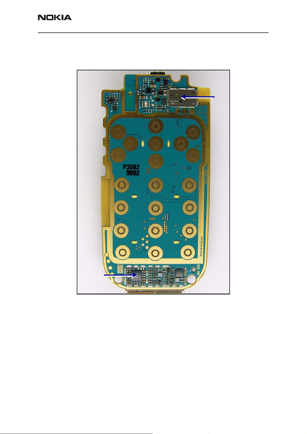
Introduction
The 2366i mobile terminal is based on a tri-mode, code division multiple access or
“CDMA,” dual-band engine and a GPS receiver.
DC/DC
Converter
FM Radio
IC (Not
used)
Figure 1: PWB components - top
Issue 2 - February 2007 Company Confidential Page 5
Page 6
2366i (RM-155)
RF Description and Troubleshooting
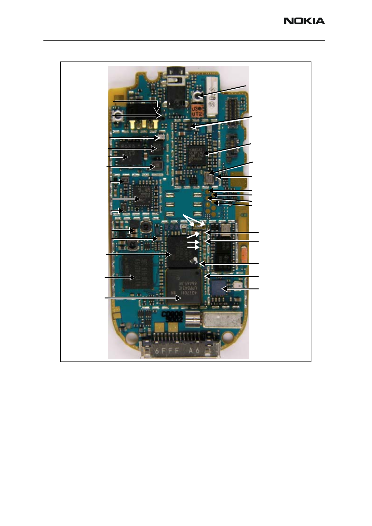
Coupler
GPS
Connector
Diplexer
PCS Duplexer
Cell/PCS PA
Cell Duplexer
Cell TX Filter
TX IC
PCS TX Filter
VCORE
TX ASIC
UEMCR D2200
Memory (D3000)
UPP (D2800)
32KHz
VFlash 1
VR3
VANA
GPS LNA
RX circuits
G7100
19.2MHz
VPP
FBus Tx
MBus Tx/Rx
FBus Rx
VR1A
VR1B
VIO
VSIM
Bluetooth
Figure 2: PWB components - bottom
Preliminary RF Troubleshooting
Verify the following if the mobile terminal cannot make a call:
• The mobile terminal is in Normal or Test Mode (i.e., the mobile terminal is
searching for a signal, net server is on).
• The Preferred Roaming List (PRL) is loaded into the mobile terminal (for Normal
mode).
• The mobile terminal is tuned and has passed tuning. Read the tuning parameters
using the Read Parameters component in Phoenix. An untuned mobile terminal
has all zeros in the tuning file.
Page 6 Company Confidential Issue 2 - February 2007
Page 7

2366i (RM-155)
Nokia Customer Care RF Description and Troubleshooting
• The call box channel is set for a channel in PRL.
• The SID is correct and entered into the mobile terminal. For Test mode, SID is 4
and paging channel is: 385/Cell and 1175/PCS.
• The VCTCXO is centered properly within tuning limits as described in the
"VCTCXO Manual Tuning" section on page 42.
• The transmitter and receiver are working properly in Local mode. See "Transmitter
RF Troubleshooting"onpage10 and "Receiver RF Troubleshooting"onpage23
for detailed information.
RF Troubleshooting Equipment List
You will need the following equipment for RF troubleshooting:
• Computer with AMS version of Phoenix
• Agilent 8960 CDMA call box (or equivalent)
• Signal generator
• Power supply
• Digital multimeter
• Diagnostic test jig
• Spectrum analyzer
• AMS RF Probe, AAS-10A or AAS-10B
• Oscilloscope
• RF connectors and cables
• High impedance probe (optional)
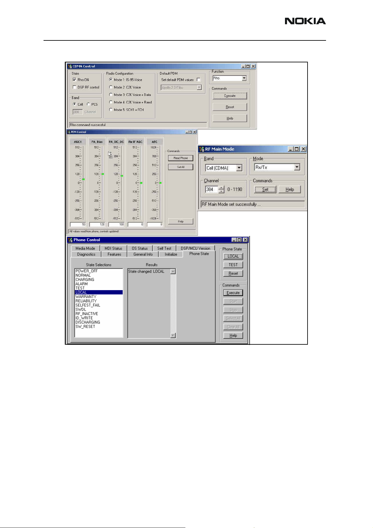
Configure Phoenix for RF Troubleshooting
1. Ensure that the phone is connected to the computer as shown in "Service
Configurations", in the Service Tools chapter.
2. Start the Phoenix software and set it up with the following controls:
• Troubleshooting > Phone Control
• Troubleshooting > RF > Main Mode
• Troubleshooting > RF > CDMA Control
• Troubleshooting > RF > PDM Control.
See Figure 3.
Issue 2 - February 2007 Company Confidential Page 7
Page 8
2366i (RM-155)
RF Description and Troubleshooting
Figure 3: Phoenix Control Setup
Page 8 Company Confidential Issue 2 - February 2007
Page 9
2366i (RM-155)
Nokia Customer Care RF Description and Troubleshooting
3. In the Phone Control window, select the Phone State tab, Local, and Execute.
4. See Table 1 for the remaining settings.
Table 1: Phoenix Settings—RF Test
For Cell For PCS
RF Main Mode window: 1. Select Cell (CDMA)
2. Select Channel (384
3. Select RX/TX mode
4. Select “Set”.
CDMA Control window: 1. Select Mode 1 (IS95/Voice)
2. De-select Default PDM
3. Select Cell Band
4. Select Rho ON
5. Select “Execute”.
PDM Control window: Set values:
• PC_DC_DC = -208
• V CTL = -361
• AGC1 = 412 mA
Set up the Spectrum Analyzer as
indicated:
Typical default values for TX RF
PDM:
Note: these are representative
values only; actual values are set
according to the tuning file. These
settings are for an output power of
20 dBm.
• Center frequency: 836.52 MHz
• Span: 100 MHz
• Amplitude: 20 dBm
• Attuenuation: auto
• BW: auto
AGC1 = -248
V CTL = -361
PC_DC_DC = 208
Current = 412 mA
1. Select PCS (CDMA)
2. Select CHannel (600)
3. Select TX/TX mode
4. Select “Set:.
1. Select Mode 1 (IS95/Voice)
2. De-select Default PDM
3. Select PCS Band
4. Select Rho ON
5. Select “Execute”.
Set values:
• PC_DC_DC = -213
• V CTL = -428
• AGC1 = 372 mA
• Center frequency: 1880 MHz
• Span: 100 MHz
• Amplitude: 20 dBm
• Attuenuation: auto
• BW: auto
AGC1 = -213
V CTL = -428
PC_DC_DC = 265
Current = 372 mA
Issue 2 - February 2007 Company Confidential Page 9
Page 10
2366i (RM-155)
RF Description and Troubleshooting
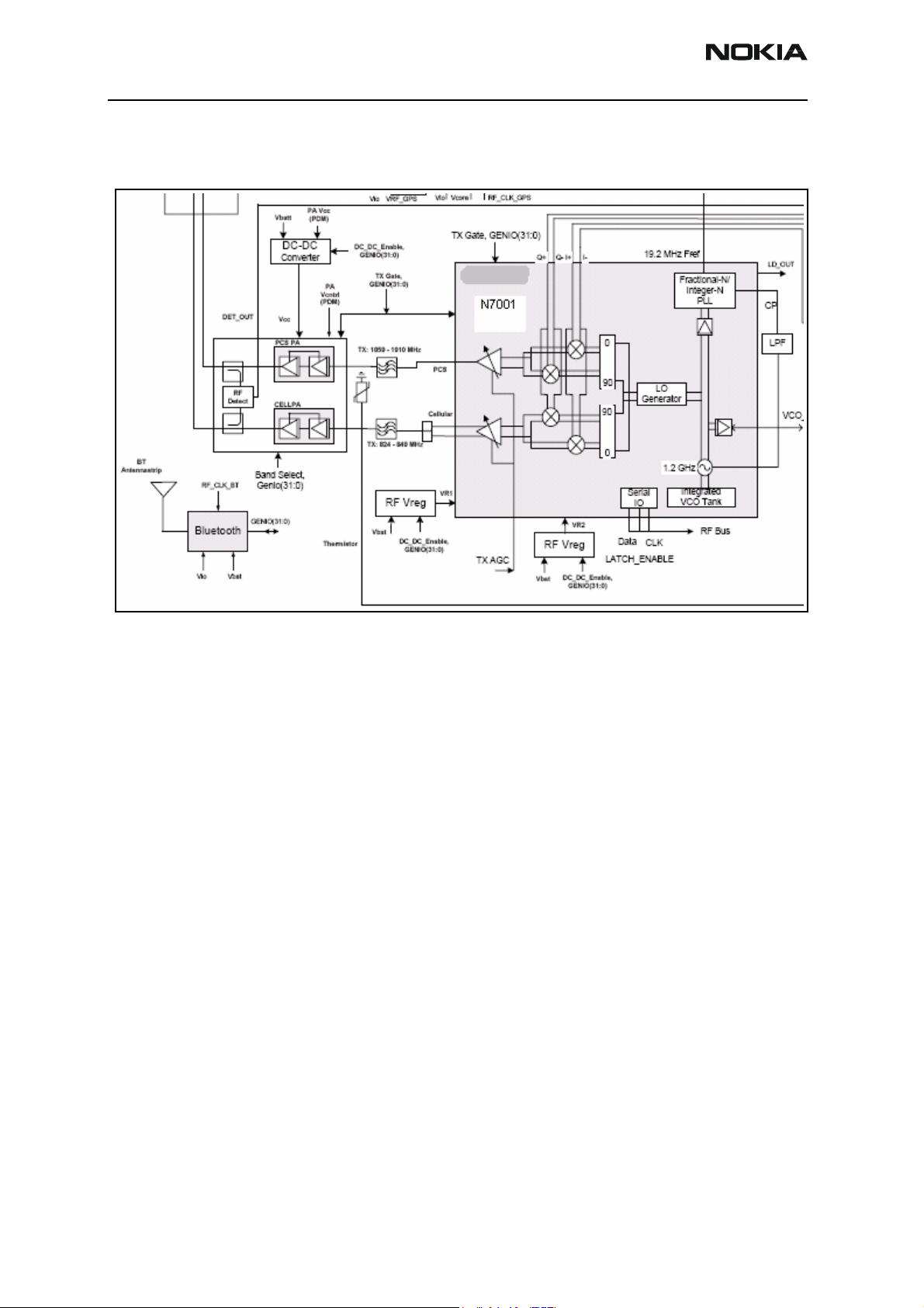
Transmitter RF Troubleshooting
Figure 4 is the block diagram for the Tx RF system.
Figure 4: Transmitter system block diagram
Page 10 Company Confidential Issue 2 - February 2007
Page 11
2366i (RM-155)
Nokia Customer Care RF Description and Troubleshooting
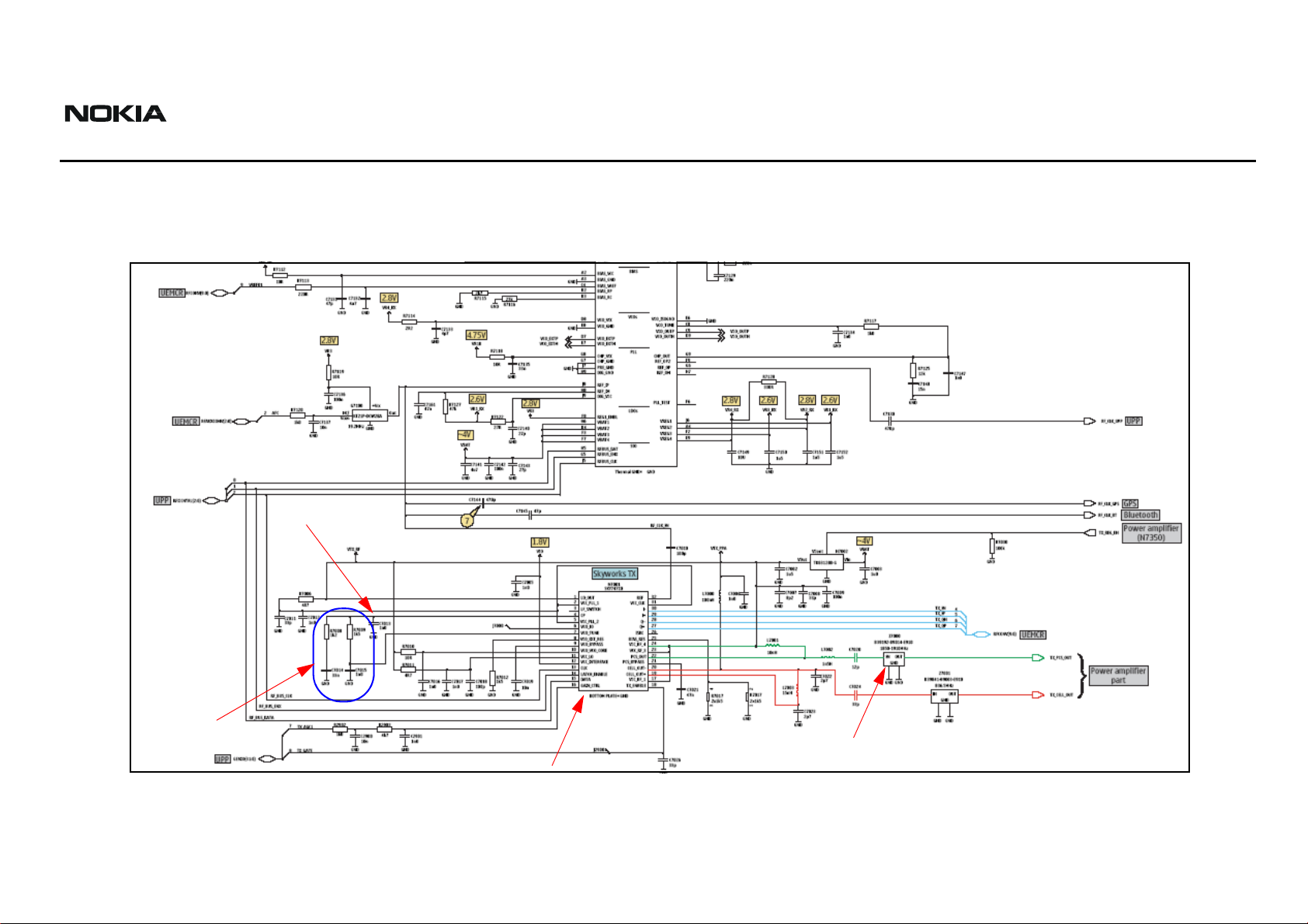
Transmitter Schematics
The following schematics are for general reference only. See the Schematics chapter for detailed versions.
TX LO Lock
Voltage
Loop
Filter
TX IC
Figure 5: Transmitter schematic
PCS TX
Filter
Cell TX Filter
Issue 2 - February 2007 Company Confidential Page 11
Page 12
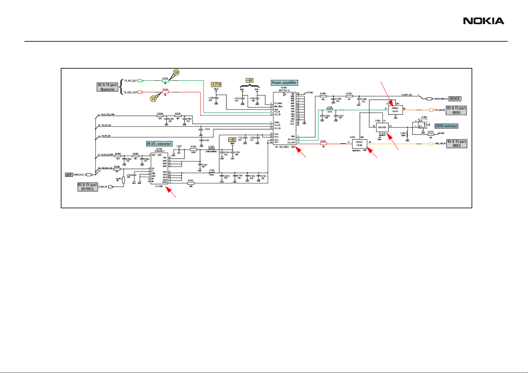
2366i (RM-155)
RF Description and Troubleshooting Nokia Customer Care
PCS Duplexer
Diplexer
PA IC
DC-DC Converter
Cell Duplexer
Figure 6: Power Amplifier schematic
Page 12 Company Confidential Issue 2 - February 2007
Page 13
2366i (RM-155)
Nokia Customer Care RF Description and Troubleshooting
Figure 7: Measurement Points and Voltages
Transmitter Troubleshooting Guidelines
Use the following guidelines when troubleshooting.
• Always perform visual inspection of PCB under microscope to check proper
placement, rotation, and soldering of components.
• Look for the presence of a well-defined CDMA modulated signal on a spectrum
analyzer at the correct frequency. If a signal is present but off frequency or the
shape looks distorted, check the synthesizer. Possibly, one of the synthesizers is
not locked or the VCO has no output signal. Check the synthesizers for proper
frequency and amplitude. See "Tx Output Spectrum" on page 19 and "Synthesizer
Troubleshooting"onpage36.
• Check that power supplies to the transmitter have the correct voltage. See "Tx RF
Component Diagram" on page 20.
• If the signal is very low in amplitude, check the probing diagram to determine
what part of the TX chain is ‘broken’. See "DC Test Points" on page 21.
• Check that AGC PDMs produce and adjust TX power within the proper limits.
Transmitter Initial Troubleshooting
Prepare the test setup:
1. Connect the RF test connector to a call box.
2. Connect the phone to the Phoenix PC
Issue 2 - February 2007 Company Confidential Page 13
Page 14

2366i (RM-155)
RF Description and Troubleshooting
3. Set up Phoenix as described in "Configure Phoenix for RF
Troubleshooting"onpage7.
DC Power Checks
Check the Tx DC points to ensure that voltages are present (see "TX RF Test
Points"onpage22).
1. Use a voltmeter to check that all VTX_RF, VTX_PPA, and VPA voltages are present.
If any voltage is missing, check for surface mount problems around the TX IC, the
PA, and the PA DC-to-DC Converter.
2. Verify that the Tx_Reg_EN, PA_DC-DC_EN, and PA_Cell/PCS_EN voltages are
present. If VTX_PPA is low and the surface mount connections are good around
the TX IC, replace the Tx Regulator (N7002). If VPA is low and surface mount
connections are good around the PA and DC-DC converter, replace the DC-DC
converter.
3. Use a voltmeter to check that VIO and VR1A voltages are present. If any is
missing, check for surface mount problems around the UEMCR. If the surface
mount connections appear good, replace the UEMCR IC.
4. Use a voltmeter to check that TxAGC1, PA_Vctrl, and PA Dc to DC PDM voltages
5. Verify that all the enable voltages (Tx_Reg_En, PA_DC-DC_EN, and PA_Cell/
Use the following sections to set up troubleshooting in Phoenix according to the band
you are using:
•"Cell Tx Setup"onpage14
•"PCS Setup"onpage16
Cell Tx Setup
Use the following procedures to prepare for Cell Tx troubleshooting using Phoenix.
1. Connect the mobile terminal to the PC via a test jig. (The bottom connector is a
2. Connect a power supply to the mobile terminal.
3. On the Phone Control dialog box, click the LOCAL button in the Phone State
from the UPP are present.
PCS_EN) are activated. If any of these signals are missing, check the surface
mount connections around the PDM lines. If the surface mount connections all
appear good, replace the UPP.
USB port.)
area to put the mobile terminal into Local Mode. (See "Configure Phoenix for RF
Troubleshooting"onpage7.)
Page 14 Company Confidential Issue 2 - February 2007
Page 15
2366i (RM-155)
Nokia Customer Care RF Description and Troubleshooting
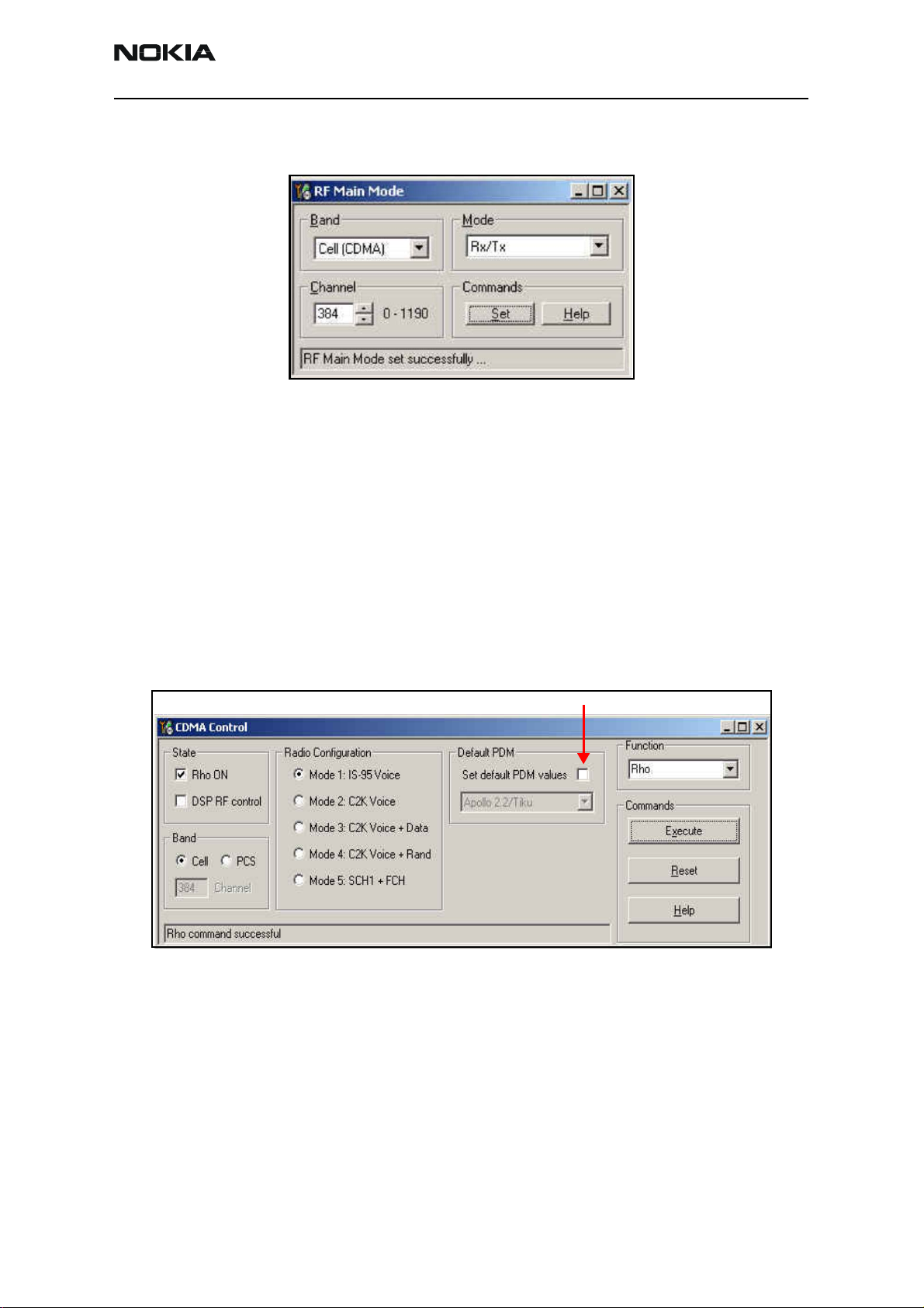
4. Open the Troubleshooting menu, point to RF, and click RF Main Mode. The RF
Main Mode dialog box appears.
Figure 8: RF Main Mode dialog box for Cell Mode
5. Select the following values on the RF Main Mode dialog box:
• Band = Cell (CDMA)
• Channel = 384
• Mode = Rx/Tx
6. Click Set.
Note: Be sure that the “RF Main Mode set successfully” message appears in
the status bar.
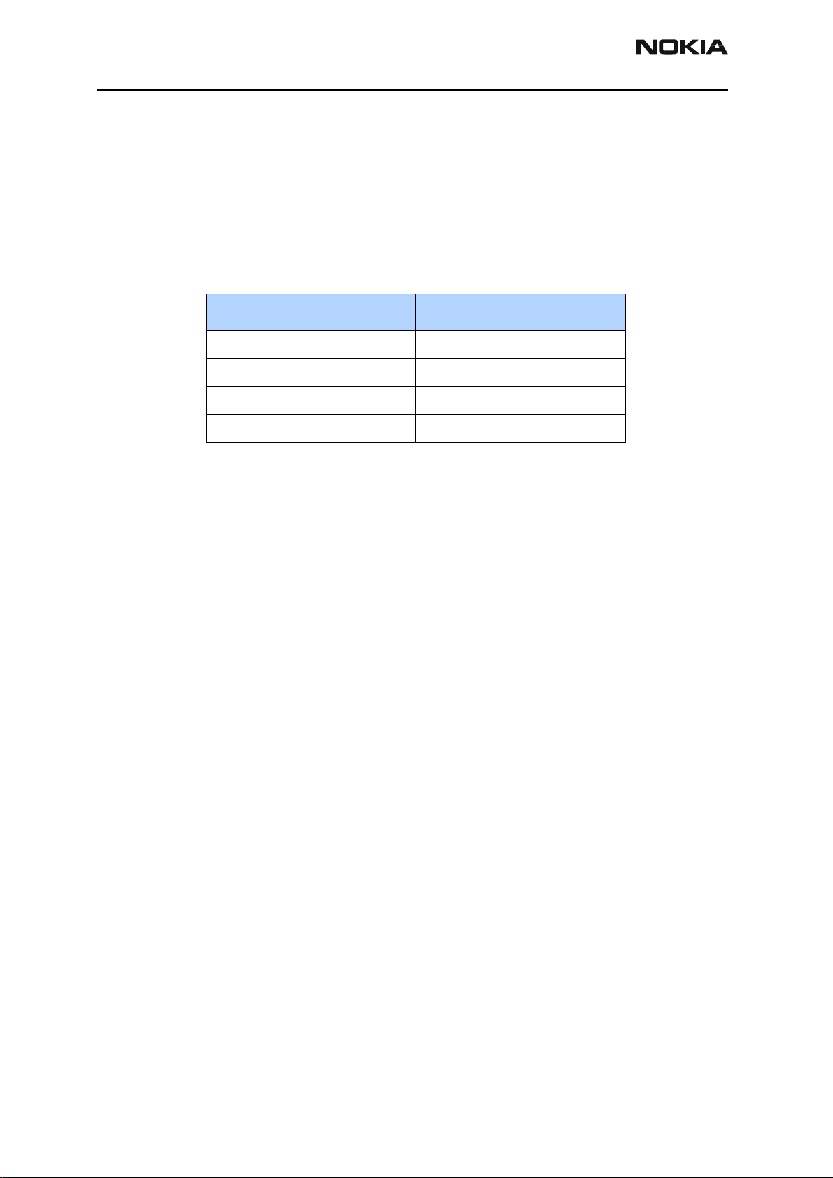
7. Open the Troubleshooting menu, point to RF, and click CDMA Control. The
CDMA Control dialog box appears.
Do NOT select this option
Figure 9: CDMA Control dialog box for Cell Tx troubleshooting
8. Select the following values:
• State = Rho ON
• Band = Cell
• Radio Configuration = Mode 1: IS-95 Voice
Note: Do NOT select the Set default PDM values option.
9. Click Execute.
Issue 2 - February 2007 Company Confidential Page 15
Page 16
2366i (RM-155)
RF Description and Troubleshooting
10. Configure the spectrum analyzer using the following values:
• Center Frequency = 836.52 MHz
• Span = 100 MHz
• Amplitude = 20 dBm
• Attenuation = Auto
Table 2: RF PDM Values
Description/Field Reference Value
AGC1 -248
V ctl -361
PA_DC_DC 208
Current 412mA
PCS Setup
Use the following procedures to prepare for PCS Tx troubleshooting using Phoenix.
1. Connect an RF test connector to a call box.
2. Connect the mobile terminal to the PC via a test jig. (The bottom connector is a
USB port.)
3. Connect a power supply to the mobile terminal.
4. Open the Troubleshooting menu, and point to Phone Control. The Phone
Control dialog box appears. ("Configure Phoenix for RF
Troubleshooting"onpage7.)
5. Click the LOCAL button in the Phone State area to put the mobile terminal into
Local Mode.
6. Open the Troubleshooting menu, point to RF, and click RF Main Mode. The RF
Main Mode dialog box appears. (See "Configure Phoenix for RF
Troubleshooting"onpage7.)
7. Select the following values on the RF Main Mode dialog box:
• Band = PCS (CDMA)
• Channel = 600
• Mode = Rx/Tx
8. Click Set.
Note: Be sure that the “RF Main Mode set successfully” message appears in
the status bar.
9. Open the Troubleshooting menu, point to RF, and click CDMA Control. The
CDMA Control dialog box appears. (See Figure 9 on page 15.)
Page 16 Company Confidential Issue 2 - February 2007
Page 17
2366i (RM-155)
Nokia Customer Care RF Description and Troubleshooting
10. Select the following values on the CDMA Control dialog box.
• State = Rho ON
• Band = PCS
• Radio Configuration = Mode 1: IS-95 Voice
Note: Do NOT select the “Set default PDM values” option.
11. Click Execute.
12. Open the Troubleshooting menu, point to RF, and click PDM Control.
13. Configure the spectrum analyzer using the following values:
• Center Frequency = 1880 MHz
• Span = 100 MHz
• Amplitude = 20 dBm
• Attenuation = Auto
• BW = Auto
Table 3: RF PDM Values
Description/Field Reference Value
AGC1 -136
V ctl -428
PA_DC-DC 265
Current 372mA
Transmitter RF Troubleshooting Procedures
After Phoenix is set up using either the Cell, or PCS setup procedures, use the following
procedures to troubleshoot the Transmitter RF section:
1. Using an oscilloscope, check the I and Q input modulation wave forms at test
points. See "Tx RF Components of the PWB"onpage20. They should all be
present with an AC swing of about 500mVpp, with an offset of +1.5 V dc.
• If one or more waveforms is missing, look for SMD problems around these
resistors.
• If the SMD is good, replace the UEMCR.
2. Use an AAS-10 RF probe to probe the Cell Tx output of the Tx IC. See Figure 10
for setup parameters and a typical display.
• If there is no RF or low RF, look for a faulty SMD around the Tx IC N7001.
• If the SMD is okay, replace the N7001 TX IC.
Issue 2 - February 2007 Company Confidential Page 17
Page 18

2366i (RM-155)
RF Description and Troubleshooting
3. Probe the PA input.
• If the level is low, look for an SMD issue on the Tx SAW filter.
• Reflow or replace the filter as necessary.
4. Probe the PA output.
• If the RF is missing or low, look for Vbat, VCC_PA, and VR1A voltages and
SMD issues on and around the PA IC N7300.
• If these are okay, replace the PA IC N7300.
5. Probe the duplexer output.
• If the RF is missing or low, reflow or replace the duplexer.
6. Probe the coupler output.
• If the RF is missing or low, reflow or replace the coupler.
7. Probe the diplexer output.
• If the RF is missing or low, reflow or replace the diplexer Z7301.
Failed Test: Tx PA Detector
Use the following steps if you encounter a failed test for the Tx PA detector:
8. Use Phoenix to set the mobile terminal into Local Mode and activate the Tx with
default output power.
• The output power at the RF test connector should be 20dBm ± 4dB. If not,
adjust the PDM values or troubleshoot per procedure above.
9. Using a voltmeter on DC, probe the detector output at C7300. The voltmeter
should read approximately 0.86 V. If not, replace N7300.
Page 18 Company Confidential Issue 2 - February 2007
Page 19

2366i (RM-155)
Nokia Customer Care RF Description and Troubleshooting
Tx Output Spectrum
Following is the correct output of the mobile terminal on a spectrum analyzer with
100MHz span. Note that if you are using the AAS-10 probe with the mobile terminal
connected to the call box, the amplitude should be approximately -7dBm at the antenna
test point on the top of the PWB.
Figure 10: Correct output spectrum
Following is an example of incorrect output.
Figure 11: Incorrect output spectrum
Issue 2 - February 2007 Company Confidential Page 19
Page 20

2366i (RM-155)
RF Description and Troubleshooting
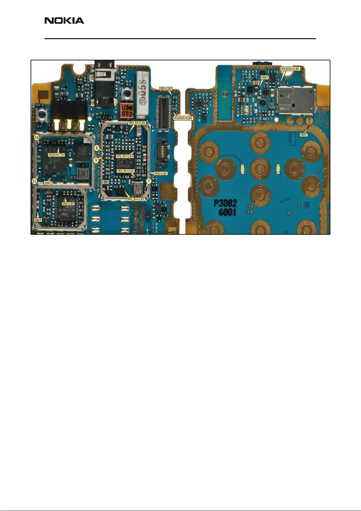
Tx RF Component Diagram
Following are the Tx RF components.
Cell TX SAW Filter
PCS TX SAW Filter
TX IC
Cell Duplexer
Tx Regulator
PCS Duplexer
DC/DC Converter (Top Side)
Diplexer
DUALBAND PA IC
Do not remove shield when checking DC/DC converter.
C7311 is DC/DC output voltage.
Figure 12: Tx RF Components of the PWB
Page 20 Company Confidential Issue 2 - February 2007
Page 21

2366i (RM-155)
Nokia Customer Care RF Description and Troubleshooting
DC Test Points
Figure 14 shows the DC test points.
TX Powe4r Detector Output (DCout)
PCS:
<0.4 V @ <5 dBm
0.59 V @ 15 dBm
1.1 V @ 23 dBm
Cell:
<0.35 V @ <5 dBm
VTX_PPA: 2.8 V
TX_REG_EN: 1.8 V
VIO 1.78V
PA_PCS_EN: 1.8 V
VR1A 4.75V
0.56 V @ 15 dBm
1.1 V @ 23 dBm
PA VCtrl PDM: 0-1.8 V
TX LO Lock
Voltage 1.3 V
VTX_RF: 2.8 V
PA_CELL_EN: 1.8 V
VPA(DC-DC Converter):
~3.2V
Tx Pwr Detector:
(See Chart Above)
Figure 13: DC Test Points 1
PA_DC-DC_EN: 1.8 V
Issue 2 - February 2007 Company Confidential Page 21
Page 22

2366i (RM-155)
RF Description and Troubleshooting
TX RF Test Points
Figure 14: TX DC Test Points 2
These points were measured on a Spectrum Analyzer and are peak values. To obtain Channel Power
(log 1.25 MHz/30 kHz), add 16 dB. See Table 2 for PDM values for Cell and PCS.
Figure 15: TX RF Test Points
Page 22 Company Confidential Issue 2 - February 2007
Page 23

2366i (RM-155)
Nokia Customer Care RF Description and Troubleshooting
Figure 16: RF Test Points (continued)
Receiver RF Troubleshooting
Note the following points when troubleshooting the receiver section:
• There is a separate LNA for 800MHz (Cell) and 1900MHz (PCS), each integrated
into the RX IC.
• The mixers are also integrated into the RX IC
• The RF section uses a dual RX SAW filter, with both filters contained in a single
package.
Issue 2 - February 2007 Company Confidential Page 23
Page 24

2366i (RM-155)
RF Description and Troubleshooting Nokia Customer Care
Receiver Block Diagram
Figure 17 is the Receiver System block diagram.
Figure 17: Receiver System block diagram
Page 24 Company Confidential Issue 2 - February 2007
Page 25

2366i (RM-155)
Nokia Customer Care RF Description and Troubleshooting
Receiver Schematics
The following schematics are for general reference only. See the Schematics chapter for detailed versions.
Cell/PCS LNAs
Cell/PCS RF
SAW filter
Cell/PCS
Demodulators
I and Q Baseband
outputs
RX Synthesizer Loop
19.2 MHz
VCTCXO
RX DC Regulators
19.2 MHz
VCTCXO
Filter
Figure 18: Receiver schematic
Issue 2 - February 2007 Company Confidential Page 25
Page 26

2366i (RM-155)
RF Description and Troubleshooting
RF AGC Status
When configuring the values on the RF AGC Status dialog box, note the following:
• The RF AGC status functionality only works in Call Mode.
•In the PLL Lock Status area, bright green indicates a locked PLL and dark green
indicates an unlocked PLL.
• Clicking the Update Now button updates the screen once.
• Clicking the Auto Update button updates the screen every second continuously.
RSSI
Tx Power
AFC PDM
LNA Gain
(High (Red)/Low)
Rx BBA Gain
Bright Green indicates Locked PLL
Dark Green indicates unlocked PLL
Single-tone
Updates
when clicked
Detector status
(disabled/below
/above)
Figure 19: RF AGC Status Dialog Box
Page 26 Company Confidential Issue 2 - February 2007
Page 27

2366i (RM-155)
y
Nokia Customer Care RF Description and Troubleshooting
Figure 20: RF AGC Status Dialog Box (continued)
Turning on the Receive Path
Use the following steps to turn on the Receive (Rx) path using Phoenix.
1. On the Phone Control dialog box, click the LOCAL button in the Phone State
area to put the mobile terminal into Local Mode.
PA AGC
PDM
PA_DC-DC
PDM
Tx AGC1
PDM settings
screen automaticall
Band selection
Updates
Figure 21: Phone Control dialog box
2. Click the Execute button.
Issue 2 - February 2007 Company Confidential Page 27
Page 28

2366i (RM-155)
RF Description and Troubleshooting
3. Depending on the band, use the applicable settings from the table below on the
RF Main Mode dialog box.
Table 4: RF Main Mode Dialog Box Settings
Band Mode Channel
AMPS (not used) Rx = 881.52 MHz 384
Cell Rx = 881.52 MHz 384
PCS Rx = 1960 MHz 600
AMPS
(not
used)
Cell
PCS
Figure 22: RF Main Mode dialog boxes for AMPS, Cell, and PCS
Page 28 Company Confidential Issue 2 - February 2007
Page 29

2366i (RM-155)
Nokia Customer Care RF Description and Troubleshooting
Switching the Rx Gain States
Use the RF Gen I/O dialog box to switch the gain state (Hi and Lo) for CDMA and AMPS
modes.
Hi Gain (Default)
State at power up
Low Gain State
Cell
AMPS
(not used)
PCS
CDMA
Figure 23: RF Gen I/O dialog box
Receiver Diagnostic Signal Tracing
Use the following information to trace the received signal through the receiver chain:
• An RF signal generator is recommended; however, an Agilent call box 8960 may
also be used. For the 8960, press the CALL SETUP key, soft key Active Cell, and
then select CW.
• Inject a CW signal for PCS (1960.3 MHz) or Cell (881.82 MHz) at a fixed –65dBm
power level.
• Take measurements with the AAS-10 probe.
• Signal levels are approximate, and accuracy may be ± 2dB or more, depending on
position and grounding of probe.
Issue 2 - February 2007 Company Confidential Page 29
Page 30

2366i (RM-155)
RF Description and Troubleshooting
Receiver DC and RF Test Points
ANT Connector
(Rx RF Input)
VR2 RX
2.7 V
VREF01
1.35 V
VR3_RX
2.6 V
VR3
2.7 V
Figure 24: Antenna connection (Rx RF input)
VR4_RX
2.72 V
VCO Control
Voltage
1.6 V PCS Ch. 600
1.2 V Cell Ch. 384
VR1_RX
2.6 V
Vbat
3.7 V
Figure 25: Receiver DC Test Points—Component Identification
Page 30 Company Confidential Issue 2 - February 2007
Page 31

2366i (RM-155)
Nokia Customer Care RF Description and Troubleshooting
VR2 RX
2.7 V
VREF01
1.35 V
VR3_RX
2.6 V
VR3
2.7 V
V4_RX
2.72 V
VCO Control Voltage
1.6 V PCS Ch. 600
1.2 V Cell Ch. 384
VR1_RX
2.6 V
Vbat
3.7 V
Figure 26: Receiver DC Test Points—Location
Issue 2 - February 2007 Company Confidential Page 31
Page 32

2366i (RM-155)
RF Description and Troubleshooting
Cell LNA output
-68 dBm
PCS DMD
Differential
Inputs
-80 dBm
Cell DMD
Differential
inputs,
-72 dBm
Cell LNA input
-71 dBm
881.52 MHz
PCS LNA input
-82 dBm
1960 MHz
PCS LNA output
-81 dBm
1960 MHz
VCO Control
Voltage
1.6 V PCS Ch. 600
1.2 V Cell Ch. 384
VCTCXO Output
19.2 MHz @ -8 dBm
Figure 27: Receiver RF Test Points — Component Identification
Page 32 Company Confidential Issue 2 - February 2007
Page 33

2366i (RM-155)
Nokia Customer Care RF Description and Troubleshooting
Cell LNA output
-68 dBm
PCS DMD
Differential
Inputs
-80 dBm
Cell DMD
Differential
inputs,
-72 dBm
Cell LNA input
-71 dBm
881.52 MHz
PCS LNA input
-82 dBm
1960 MHz
PCS LNA output
-81 dBm
1960 MHz
VCO Control
Voltage
1.6 V PCS Ch. 600
1.2 V Cell Ch. 384
VCTCXO
Output
19.2 MHz @ -8 dBm
Figure 28: Receiver RF Test Points — Location
There are two common explanations for a Rx Front-end IC failure consisting of high
current in Local Mode with just the Rx turned on:
• No presence of a LO signal
• Input impedance drop is shorting out one of the DC supply pins to the chip
IMPORTANT: You must check for both conditions before replacing the chip. If you
have no LO signal, refer to "GPS Troubleshooting"onpage44. If you have a significant
supply voltage drop on one of the supply pins, then replace the Rx Front-end IC.
Table 5: Rx Front-end IC Conditions and Supply Currents
Condition: Local Mode, Set
Rx Only in RF Main Mode
Good mobile terminal 100mA
No UHF LO signal present 254mA
Supply Current
(From Power Supply)
Power input pin shorted 255mA
Issue 2 - February 2007 Company Confidential Page 33
Page 34

2366i (RM-155)
RF Description and Troubleshooting
Receiver I and Q Test Points
Figure 29 shows the test points for the receiver I and Q channels.
Note: the Baseband signal has a 1.35 V dc offset.
Rx Test points (4)
Figure 29: Receiver Test Points—I and Q Channels
Use the following procedure to check the path from RF to I and Q output.
1. Set the mobile terminal to Local Mode, using Phoenix (Phone Control > Phone
State tab > LOCAL.
2. Turn on only the RX path for the band to be checked (Cell or PCS), using Phoenix.
3. Set the receiver band and channel as shown in Table 6.
Table 6: Settings for Receiver Band and Channel
Band Channel Frequency
CELL 384 881.52
PCS 600 1960
4. Inject a signal at the frequency and level shown in Table 7.
Table 7: Injection Frequencies and Levels
Band
CW Signal
Frequency
CW Signal
Level
Level of 300 kHz
I Q Tone (± 2 dB)
CELL 881.82 MHz -75 dBm -33 dBm
PCS 1960.3 MHz -95 dBm -37 dBm
Page 34 Company Confidential Issue 2 - February 2007
Page 35

2366i (RM-155)
Nokia Customer Care RF Description and Troubleshooting
5. Measure the level of a 300 kHz tone on the Spectrum Analyzer. The tone should
be ± 2 dB of the value shown in Table 7.
Figure 30 shows the typical traces on the Spectrum Analyzer for each band.
1
Cell
(1) 300-kHz tone @ -33 dBm
Figure 30: I Q tones for Cell and PCS
2
PCS
(2) 300-kHz tone @ -37 dBm
Issue 2 - February 2007 Company Confidential Page 35
Page 36

2366i (RM-155)
RF Description and Troubleshooting
Synthesizer Troubleshooting
Faulty synthesizers can cause both Rx and Tx failures during tuning, in addition to the
VCTCXO tuning. However, first check for the presence of various LO signals and their
proper levels. If everything fails, it may be necessary to check the reference clock
(19.2MHz) which is needed for the mobile terminal to power up. The 19.2MHz signal is
also important because the N7100 Receiver IC is sensitive enough to pick up a very weak
19.2MHz clock, resulting in intermittent problems such as a constant mobile terminal
reset.
The Synthesizer has the following characteristics:
• TX Local Oscillator (LO): 1099.6–1131.08 MHz for the CELL band, and 1233.333–
1273.333 MHz for the PCS band, with the offset phase-locked loop (PLL) inside
the TX IC N7001.
• LO frequency calculation:
• CELL: LO = TXfreq x (4/3)
• PCS: LO = TXfreq x (2.3)
If the PLL frequencies are incorrect, the following causes are possible:
• Power supplies to the PLL portion
• Control line to voltage-controlled oscillator (VCO).
• Loop filter or resonator components are missing or incorrectly installed.
• 19.2 MHz reference clock signal is missing or low.
VCTXCO Troubleshooting
The VCTXO operates on 19.2 MHz and provides the reference signal for the synthesizer. If
the 19.2 signal fails, the mobile terminal does not power up.
Use the following procedure to troubleshoot the VCTXO:
1. Check for the presence of the signal at the following points (see figure x):
a. RF_CLK_IN, clock reference to the TX RF IC should be ~ 8 dBm.
b. RF_CLK_UPP, clock reference for the UPP IC, should be ~ 3 dBm.
2. If the VCTXO signal is not present at any of these points, check the voltage at
VR3 (R7119), the main supply line for the VCTXO. The signal should be 2.7 V dc.
See figure x.
3. Check the AFT voltage. The signal should be between 0 and 2.5 V dc, and should
be adjustable by operating the AFC slider on the RF PDM control window in
Phoenix (see figure y).
4. If the AFC voltage is not present, check the UEMCR IC.
5. If the frequencies coming from the phase locked loop (PLL) are incorrect, the
following possible causes exist:
Page 36 Company Confidential Issue 2 - February 2007
Page 37

2366i (RM-155)
Nokia Customer Care RF Description and Troubleshooting
• Missing or low power supply voltage to the PLL section
• Fault in the control line to the voltage controlled oscillator (VCO).
• Loop filter or resonator components are missing or are incorrectly installed.
• The 19.2 MHz reference clock signal is missing (mobile terminal does not
boot up) or low (possible resets of the mobile terminal).
• Failure of the TX IC (N7100) or the VCTXO.
Synthesizer Schematic
The following schematics are for general reference only. See the Schematics chapter for
detailed versions.
Lock Voltage
UHF Loop Filter
Figure 31: Synthesizer schematic
Issue 2 - February 2007 Company Confidential Page 37
Page 38

2366i (RM-155)
RF Description and Troubleshooting
Synthesizer Troubleshooting Setup
Use the following steps to troubleshoot the synthesizer using Phoenix:
1. On the Phone Control dialog box, click the LOCAL button in the Phone State
area to put the mobile terminal into Local Mode. See Figure 32
Figure 32: Phone Control dialog box
2. Select the following values on the RF Main Mode dialog box as shown below:.
Table 8: RF Main Mode Dialog Box Settings
Synthesizer Band Mode Channel
Cell (1115.36 MHz) Rx/Tx 384 -80 dBm
UHF
PCS (1253.333 MHz) Rx/Tx 600 -74 dBm
Signal
Level
Figure 33: Phone Control dialog box
Page 38 Company Confidential Issue 2 - February 2007
Page 39

2366i (RM-155)
Nokia Customer Care RF Description and Troubleshooting
Synthesizer Troubleshooting
Use the following procedure to troubleshoot the Synthesizer.
1. Measure the Local Oscillator (LO) signal by probing the TX IC (N7001) with the
AMS Probe at the location shown in Figure 34. Table 8 shows the required signal
levels. Figure 35 shows a typical spectrum display for PCS; Figure 36 shows the
display for a CELL signal.
Vbat
3.7 V
Measure Local
Oscillator signal here
VTX_RF
2.8 V
VIO
1.8 V
Vcc LO
2.3 V
Vcc VCO Core
2.8V
Figure 34: Test Points—TX UHF Local Oscillator N7001
Lock voltage: DC
between
1.0 - 1.8 V
AMS Probe
Signal: Channel 600
1253.333 MHz
~ -73 dBm
Analyser Settings:
Center: 1253.333 MHz Span: 200 kHz
RBW: 1 kHz VBW: 300 Hz
Figure 35: PCS TX LO—Typical Spectrum
Issue 2 - February 2007 Company Confidential Page 39
Page 40

2366i (RM-155)
RF Description and Troubleshooting
AMS Probe
Signal: Channel 600
1115.36 MHz
~ -80 dBm
Analyser Settings:
Center: 1115.36 MHz Span: 200 kHz
RBW: 1 kHz VBW: 300 Hz
Incorrect PLL Frequencies
Following are some possible causes for incorrect PLL frequencies:
• Missing or low power supply voltage to the PLL section
• Fault in the control line to the voltage controlled oscillator (VCO).
• Loop filter or resonator components are missing or are incorrectly installed.
• The 19.2 MHz reference clock signal is missing (mobile terminal does not
boot up) or low (possible resets of the mobile terminal).
• Failure of the TX IC (N7001) or the VCTXO (G7100).
Figure 36: Cell TX LO—Typical Spectrum
Page 40 Company Confidential Issue 2 - February 2007
Page 41

2366i (RM-155)
Nokia Customer Care RF Description and Troubleshooting
AFC Voltage Troubleshooting
Use the following steps to monitor the AFC voltage.
1. In Phoenix, open the RF PDM dialog box.
Figure 37: RF PDM dialog box for AFC troubleshooting
Figure 38 shows a partial schematic of the R7201.
R7120
Figure 38: Partial schematic showing the R7201
2. Measure the DC voltage at R7120. The following typical voltages are observed.
• AFC PDM[0]=1.3 V
• AFC PDM[-1024]=0 V
• AFC PDM[1023]=2.5 V
Issue 2 - February 2007 Company Confidential Page 41
Page 42

2366i (RM-155)
RF Description and Troubleshooting
VCTCXO Manual Tuning
You can manually tune the VCTCXO to verify when a mobile terminal is tuned incorrectly
or if mobile terminal cannot make a call. Monitor the RF signal at the mobile terminal’s
LNA output. See Figure 39 and Figure 40 for
1. On the Phone Control dialog box, click the LOCAL button in the Phone State
area to put the mobile terminal into Local Mode. (see "Configure Phoenix for RF
Troubleshooting"onpage7) for an example of the Phone Control dialog box.)
2. Click the Execute button.
3. In Main Mode:
a. Select CELL_PCS;
b. Select Channel (384 for CELL, 600 for PCS); (See "Configure Phoenix for RF
Troubleshooting"onpage7)
4. In the CDMA Control window:
a. Select Mode 1 (IS95/Voice
b. De-select Default PDM
c. Select the appropriate band (CELL or PCS)
d. Select Rho ON
e. Click “Execute. The CDMA pedestal output should be visible on the Spectrum
Analyzer at the appropriate band and channel frequency.
f. De-select Rho ON and select “Execute.
g. Select “Set” in the Main Mode window. A CW output signal is generated.
• Set the center frequency of the Spectrum Analyzer to 836.52MHz and the
span to 2MHz initially. Establish a marker at 3526.08 MHz for CELL, or 3920
Mhz for PCS.
• Set the span to 100 kHz.
5. Use the RF PDM component to adjust the AFC to center the VCTCXO. The tuning
range is approximately ±50kHz.
6. Adjust the AFC so that the output signal is within ±150MHz. If using a spectrum
analyzer, narrow the span to 1kHz or less.
7. If the VCTXO does not tune, but its power supply voltages and control voltages
are present, replace the VCTXO IC (G7100).
8. If the voltages are not present, check that the surface mounting connections are
good. If so, replace the UEMCR IC (D2200).
Page 42 Company Confidential Issue 2 - February 2007
Page 43

2366i (RM-155)
2
o
3
0
r
2
Nokia Customer Care RF Description and Troubleshooting
Signal Measured at output of LNA CELL
dBm
PDM AFC=ZeroPDM AFC=1023PDM AFC=-1024
0
-10
-20
-30
-40
-50
-60
-70
-80
-90
-100
1
Centre: 3.526080 GHz Span: 100.000000 kHzAtten: 10 dB
Res BW: 1 kHz Vid BW: 1 kHz Sweep: 300 ms
7/25/2006 4:56:10 PM HP8595EAFC Control CELL.spt
2
3
1
PDM AFC=-10
3.526037 GHz
-40.11 dBm
2
PDM AFC=Zer
3.526079 GHz
-40.34 dBm
3
PDM AFC=102
3.526117 GHz
-40.24 dBm
dBm
0
-10
-20
-30
-40
-50
-60
-70
-80
-90
-100
Figure 39: Tx Output for CELL channel 384 @ 25C
Signal Measured at output of LNA PCS
RF PDM AFC=ZeroRF PDM AFC=-1024RF PDM AFC=1024
1
2
Centre: 3.920000 GHz Span: 100.000000 kHzAtten: 10 dB
3 3
Res BW: 1 kHz Vid BW: 1 kHz Sweep: 300 ms
7/25/2006 3:50:28 PM HP8595EAFC Control.spt
Figure 40: Tx Output for PCS channel 600 @ 25C
Figure 41: UHF Synthesizer Schematic
1
RF PDM AFC=-1
3.919953 GHz
-39.69 dBm
2
RF PDM AFC=Ze
3.920000 GHz
-39.88 dBm
RF PDM AFC=10
3.920043 GHz
-39.76 dBm
Issue 2 - February 2007 Company Confidential Page 43
Page 44

2366i (RM-155)
RF Description and Troubleshooting
GPS Troubleshooting
GPS RF Block Diagram
FilterFilter
LNA
TCXO
16.368MHz
GPS RF Schematic
The following schematic is for general reference only. See the Schematics chapter for a
detailed version.
IF = 4.092MHz
AGC
Amp
Synthesiser
GPS RF
Figure 42: GPS block diagram
2nd RF filter
GPS LNA
TRF5101
1st RF filter
4
ADC
Cellular Baseband
Rx Data
Out
GPS
Baseband
Ref Clk
GPS RF chip
RF input
GPS TCXO
Figure 43: GPS RF schematic
Page 44 Company Confidential Issue 2 - February 2007
Page 45

2366i (RM-155)
Nokia Customer Care RF Description and Troubleshooting
GPS Troubleshooting Setup
Use the following steps to set up GPS signal using Phoenix.
1. On the Phone Control dialog box, click the LOCAL button in the Phone State
area to put the mobile terminal into Local Mode.
Figure 44: Phone Control dialog box
2. Click Execute.
3. Inject a -110dBm tone at 1575.52MHz at the GPS connector (X6250) with a
signal generator or call box.
CW tone
Figure 45: GPS connector (X6250)
Issue 2 - February 2007 Company Confidential Page 45
Page 46

2366i (RM-155)
RF Description and Troubleshooting
4. Open the Troubleshooting menu, and click GPS Quick Test. The GPS Control
dialog box appears
5. In the Test State field, ensure that Galvanic is selected.
6. Click select Start test.
See Figure 47 for the GPS test points.
HW Self Test Failure
If the test fails, repeat steps 1—6. If the test fails again, continue with the following selftest failure troubleshooting:
1. Verify the DC voltages at VRF_GPS and VDD_IO_GPS.
2. Inspect all GPS circuit elements around the GPS BB chip (D6200).
3. If the elements pass a visual inspection, replace the N6200.
Oscillator Test Failure
1. Inspect all GPS circuit elements around the N2651.
2. If the elements pass a visual inspection, replace the G6250.
Figure 46: GPS Control dialog box
Page 46 Company Confidential Issue 2 - February 2007
Page 47

2366i (RM-155)
Nokia Customer Care RF Description and Troubleshooting
CW (Mode 3) Test Failure
1. Check that the signal generator is on and sourcing a signal to the GPS RF input
port (X6250).
2. Inspect all GPS RF Circuit elements
3. Inspect all GPS Circuit elements around N6251.
4. If the elements pass a visual inspection and the RF is good, replace the GPS RF IC
(N6251).
GPS DC Test Points
VDD_IO_GPS:
1.8 V
VRF_GPS:
2.8 V
TCXO Vcc:
2.8 V
Figure 47: GPS DC test points
Issue 2 - February 2007 Company Confidential Page 47
Page 48

2366i (RM-155)
RF Description and Troubleshooting
GPS RF Troubleshooting Setup
Use the following steps to troubleshoot the GPS receiver.
1. On the GPS Control dialog box, click Receiver On.
Figure 48: Turning on the GPS receiver on the GPS Control dialog box
2. Click Start Test.
3. Inject a -50dBm tone at 1575.52MHz at the GPS connector (X6250) with a signal
generator or a call box. (See Figure 45.)
4. Measure the test points with an AAS-10B probe and spectrum analyzer set at
center frequency 1575.25MHz (span = 500kHz), or with a voltmeter as required.
(See Figure 49.)
Page 48 Company Confidential Issue 2 - February 2007
Page 49

2366i (RM-155)
Nokia Customer Care RF Description and Troubleshooting
GPS RF Probe Points
All point s are 1575.52 MHz,
except TCXO
4
GPS LNA out
-45 dBm
GPS LNA in
3
-63 dBm
First RF filter out
2
-65 dBm
1
First RF filter in
-62 dBm
All points are 1575.52 MHz,
except TCXO
GPS BBIC
Figure 49: GPS RF Test Points
GPS RF ASIC
GPS TCXO out
16.368 MHz
-3 dBm
Note: All probe points are 1575.52MHz except TXCO.
6
nd
2
RF filter out
-46 dBm
5
2ndRF filter in
-46 dBm
Issue 2 - February 2007 Company Confidential Page 49
Page 50

2366i (RM-155)
RF Description and Troubleshooting
Bluetooth Troubleshooting
Bluetooth Schematic
The schematic in Figure 50 is for general reference only. See the Schematics chapter for
a detailed version.
BT Antenna
Test Setup 1
Open the BT/WLAN menu, and click Bluetooth Locals. If the Phoenix connection to the
mobile terminal’s BT ASIC is ok, text such as “MCM Software”, “MM Software” is
displayed in the Version Information window.
Saw Filter
Bluetooth
ASIC N6000
Figure 50: Bluetooth schematic
Page 50 Company Confidential Issue 2 - February 2007
Page 51

2366i (RM-155)
Nokia Customer Care RF Description and Troubleshooting
If “No version information available” is displayed in the Version Information window,
there may be a Phoenix connection problem, a connection problem between the D2800
processor and the BT ASIC or the BT ASIC is not working. See item 1 in "Bluetooth
flowchart"onpage56.
Figure 51: Bluetooth Locale window
Issue 2 - February 2007 Company Confidential Page 51
Page 52

2366i (RM-155)
RF Description and Troubleshooting
Test Setup 2
After obtaining the version information, select Run to do a quick check on the BT ASIC.
The results of each self-test are displayed in the Self Tests window. If any test fails, BT
ASIC is not working properly. Change the BT ASIC.
Figure 52: Self Test area on the Bluetooth Locale window
Page 52 Company Confidential Issue 2 - February 2007
Page 53

2366i (RM-155)
Nokia Customer Care RF Description and Troubleshooting
Test Setup 3
1. After passing the self-test, setup the JBT-3, JBT-9 or a later version BT box.
2. Type the BT box’s device address into the Counterpart BT Device Address
window.
3. Select Run BER Test to run the BER loopback test. The BER result is visible in the
BER Test Results window.
4. Because this is a “go-no-go” testing, make sure the test-jig/coupler is setup
correctly. It is recommended to run couple “good” mobile terminals in order to
get better correlation. The acceptance criteria is BER<0.1%.
Issue 2 - February 2007 Company Confidential Page 53
Page 54

2366i (RM-155)
RF Description and Troubleshooting
Test Setup 4
If the mobile terminal’s BT sensitivity is not good or the setup is not calibrated
(correlated) correctly, the %BER > 0.1% which results in an error. Make sure the setup is
good (correlated with a golden mobile terminal), then see Item 2 in "Bluetooth
flowchart"onpage56.
Page 54 Company Confidential Issue 2 - February 2007
Page 55

2366i (RM-155)
Nokia Customer Care RF Description and Troubleshooting
Test Setup 5
If the mobile terminal is placed too far or the BT Tx or the Rx has problem, one of the
following error messages is visible. (See Item 2 of "Bluetooth flowchart"onpage56).
Issue 2 - February 2007 Company Confidential Page 55
Page 56

2366i (RM-155)
RF Description and Troubleshooting Nokia Customer Care
Bluetooth Troubleshooting Flowchart
Replace BT ASIC (N6000) when a particular row is still not ok at the end of a branch.
Before Probing, first perfrom visual inspection of all BT components. Look for solder bridges, tombstone, rotation, and other SMD failures.
not OK
Item 1 VDD_CORE @C6011 (1.8V) Replace BT ASIC
not OK not OK
800mV > Xtal_IN > 400mVp-p, 19.2 MHz @ C7145 Replace C7145 Replace 19.2MHz VCTCXO G7100
not OK not OK
Item 2
Does BER pass with BT Test Box (JBT-3,…)? Replace BT Filter Z6000 Replace BT ASIC
Figure 53: Bluetooth flowchart
Page 56 Company Confidential Issue 2 - February 2007
Page 57

2366i (RM-155)
Nokia Customer Care RF Description and Troubleshooting
Bluetooth DC and RF Probe Points
Figure 54 shows the Bluetooth DC and RF probe points.
Bluetooth ASIC
VDD_CORE
Xtal_in
19.2MHz
SAW Filter
Figure 54: Bluetooth DC and RF Probe points
Issue 2 - February 2007 Company Confidential Page 57
Page 58

2366i (RM-155)
RF Description and Troubleshooting Nokia Customer Care
This page intentionally left blank.
Page 58 Company Confidential Issue 2 - February 2007
 Loading...