

Page 1

Nokia Customer Care
6275/6275i (RM-154)
Mobile Terminals
RF Description and
Troubleshooting
Issue 1 - September 2006 Company Confidential ©2006 Nokia Corporation
Page 2

6275/6275i (RM-154)
RF Description and Troubleshooting
Contents Page
Introduction ..................................................................................................................................................... 5
Preliminary RF Troubleshooting ..............................................................................................................6
RF Troubleshooting Equipment List ........................................................................................................7
Transmitter RF Troubleshooting ................................................................................................................. 8
Transmitter Schematics ............................................................................................................................. 9
Transmitter Troubleshooting Guidelines .............................................................................................11
Transmitter Troubleshooting Setup ......................................................................................................11
AMPS Tx Setup ....................................................................................................................................... 12
Cell Tx Setup ........................................................................................................................................... 13
PCS Setup................................................................................................................................................. 15
Transmitter RF Troubleshooting Procedures ......................................................................................16
Failed Test: Tx PA Detector ................................................................................................................. 17
Tx Output Spectrum.............................................................................................................................. 18
Tx RF Component Diagram ................................................................................................................. 19
Tx DC Probe Points ................................................................................................................................ 19
Tx RF Probe Points................................................................................................................................. 20
DC Test Points......................................................................................................................................... 20
Receiver RF Troubleshooting .................................................................................................................... 20
Receiver Block Diagram ...........................................................................................................................21
Receiver Schematics .................................................................................................................................22
RF AGC Status ............................................................................................................................................24
Turning on the Rx Path ............................................................................................................................25
Switching the Rx Gain States ................................................................................................................27
Receiver Diagnostic Signal Tracing ......................................................................................................27
Receiver RF Probe Points..................................................................................................................... 28
Receiver IF Probe Points ...................................................................................................................... 29
Receiver DC Probe Points .................................................................................................................... 30
Receiver Logic Input Voltages ................................................................................................................31
Rx Front-End Receiver Troubleshooting .............................................................................................31
Synthesizer Troubleshooting .................................................................................................................... 33
Synthesizer Block Diagram .....................................................................................................................34
Synthesizer Schematics ...........................................................................................................................35
Synthesizer Troubleshooting Setup ......................................................................................................36
Incorrect PLL Frequencies.................................................................................................................... 37
VCTCXO Troubleshooting .........................................................................................................................37
AFC Voltage Troubleshooting .................................................................................................................38
VCTCXO Manual Tuning....................................................................................................................... 39
UHF Synthesizer Schematic ....................................................................................................................41
UHF Synthesizer Troubleshooting .........................................................................................................41
PCS UHF LO CH600 Typical Spectrum .................................................................................................43
Rho and UHF LO..................................................................................................................................... 43
CELL UHF LO CH384 Typical Spectrum ...............................................................................................44
Rho and UHF LO..................................................................................................................................... 44
Rx VHF LO (Rx Back-End IC) Troubleshooting ...................................................................................45
Tx UHF LO Schematic ...............................................................................................................................46
Tx UHF LO (Tx IC) Troubleshooting .......................................................................................................46
UHF PCS Tx LO (3700 ~ 3819.90)/2MHz Typical Spectrum ..........................................................47
Page 2 Company Confidential Issue 1 - September 2006
Page 3

6275/6275i (RM-154)
Nokia Customer Care RF Description and Troubleshooting
UHF CELL Tx LO (3296.16 ~ 3395.88)/4MHz Typical Spectrum ...................................................48
GPS Troubleshooting................................................................................................................................... 49
GPS RF Block Diagram .............................................................................................................................49
GPS RF Schematic .....................................................................................................................................49
GPS Troubleshooting Setup ....................................................................................................................50
HW Self Test Failure.............................................................................................................................. 51
Oscillator Test Failure........................................................................................................................... 51
CW (Mode 3) Test Failure.................................................................................................................... 51
GPS DC Test Points................................................................................................................................ 52
GPS RF Troubleshooting Setup........................................................................................................... 53
GPS RF Probe Points.............................................................................................................................. 54
FM Radio Troubleshooting ........................................................................................................................ 55
FM Radio Schematic .................................................................................................................................55
FM Radio Testing .......................................................................................................................................55
FM Radio Parts Layouts ...........................................................................................................................56
FM Radio Probe Points .............................................................................................................................56
Bluetooth Troubleshooting ....................................................................................................................... 57
Bluetooth Schematic ................................................................................................................................57
Test Setup 1 ................................................................................................................................................58
Test Setup 2 ................................................................................................................................................59
Test Setup 3 ................................................................................................................................................60
Test Setup 4 ................................................................................................................................................61
Test Setup 5 ................................................................................................................................................62
Bluetooth Troubleshooting Flowchart .................................................................................................63
Bluetooth DC and RF Probe Points .......................................................................................................64
Issue 1 - September 2006 Company Confidential Page 3
Page 4

6275/6275i (RM-154)
RF Description and Troubleshooting Nokia Customer Care
This page intentionally left blank.
Page 4 Company Confidential Issue 1 - September 2006
Page 5
6275/6275i (RM-154)
Nokia Customer Care RF Description and Troubleshooting
Introduction
The 6275/6275i mobile terminal is based on tri-mode, code division multiple access or
“CDMA,” dual-band engine. The variants include tri-mode terminals with and without
the GPS component.
Note: The 6275 variant is identical to the 6275i variant, except that the GPS is not
supported in the 6275 variant.
D2800
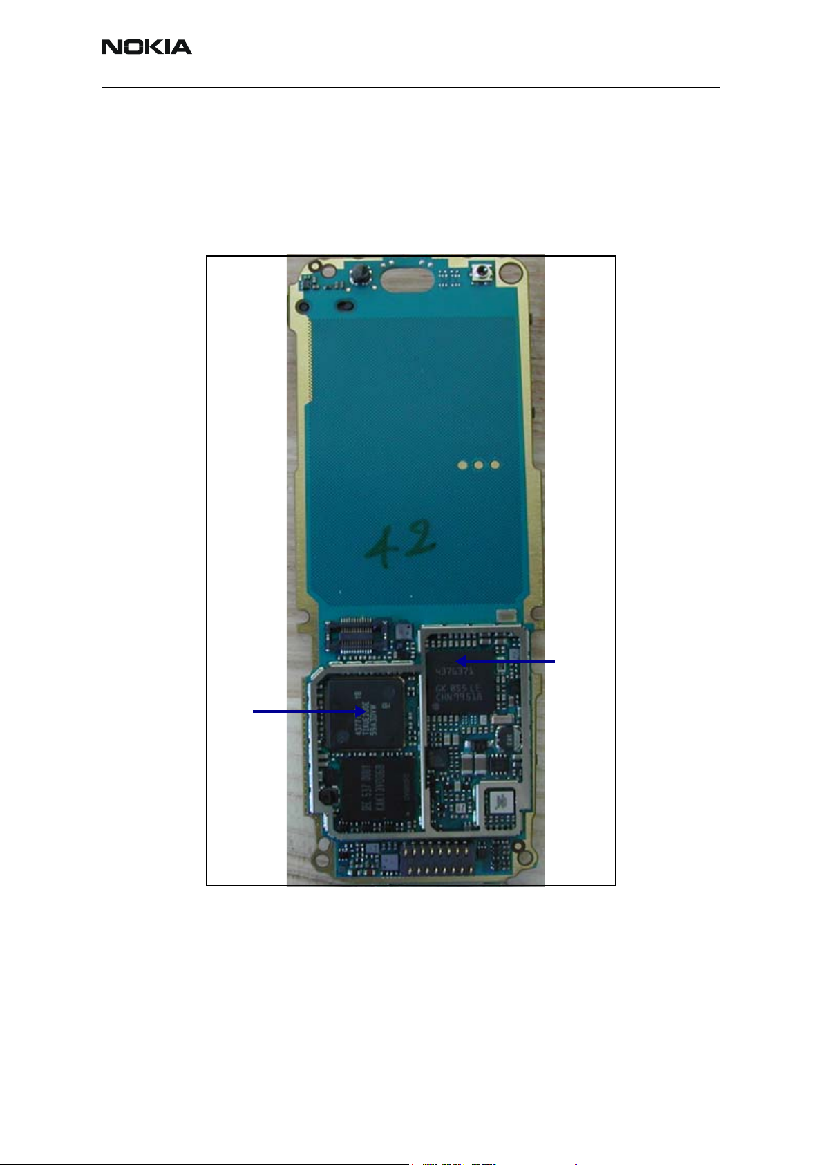
UEMEK
Figure 1: PWB components - top
Issue 1 - September 2006 Company Confidential Page 5
Page 6
6275/6275i (RM-154)
RF Description and Troubleshooting
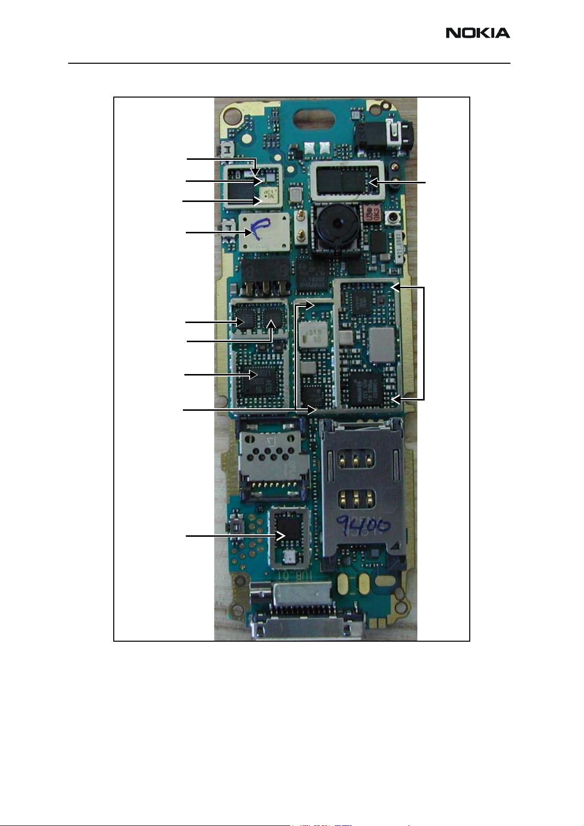
Coupler
Diplexer
Duplexer
PA DC/DC converter
PCS PA
GPS
Cell PA
TX ASIC
VCO synthesizer
Bluetooth
RX circuits
Figure 2: PWB components - bottom
Preliminary RF Troubleshooting
Verify the following if the mobile terminal cannot make a call:
• The mobile terminal is in Normal or Test Mode (i.e., the mobile terminal is
searching for a signal, net server is on).
Page 6 Company Confidential Issue 1 - September 2006
Page 7

6275/6275i (RM-154)
Nokia Customer Care RF Description and Troubleshooting
• The Preferred Roaming List (PRL) is loaded into the mobile terminal (for Normal
mode).
• The mobile terminal is tuned and has passed tuning. Read the tuning parameters
using the Read Parameters component in Phoenix. An untuned mobile terminal
has all zeros in the tuning file.
• The call box channel is set for a channel in PRL.
• The SID is correct and entered into the mobile terminal. For Test mode, SID is 4
and paging channel is: 385/Cell and 1175/PCS.
• The VCTCXO is centered properly within tuning limits as described in the
"VCTCXO Manual Tuning" section on page 39.
• The transmitter and receiver are working properly in Local mode. See "Transmitter
RF Troubleshooting"onpage8 and "Receiver RF Troubleshooting"onpage20 for
detailed information.
RF Troubleshooting Equipment List
You will need the following equipment for RF troubleshooting:
• Computer with AMS version of Phoenix
• Agilent 8960 CDMA call box (or equivalent)
• Signal generator
• Power supply
• Digital multimeter
• Diagnostic test jig
• Spectrum analyzer
• AMS RF Probe, AAS-10A or AAS-10B
• Oscilloscope
• RF connectors and cables
• High impedance probe (optional)
Issue 1 - September 2006 Company Confidential Page 7
Page 8
6275/6275i (RM-154)
RF Description and Troubleshooting
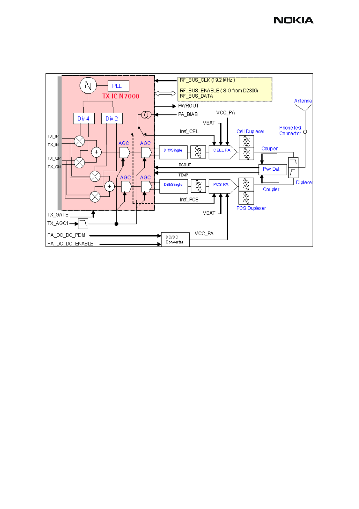
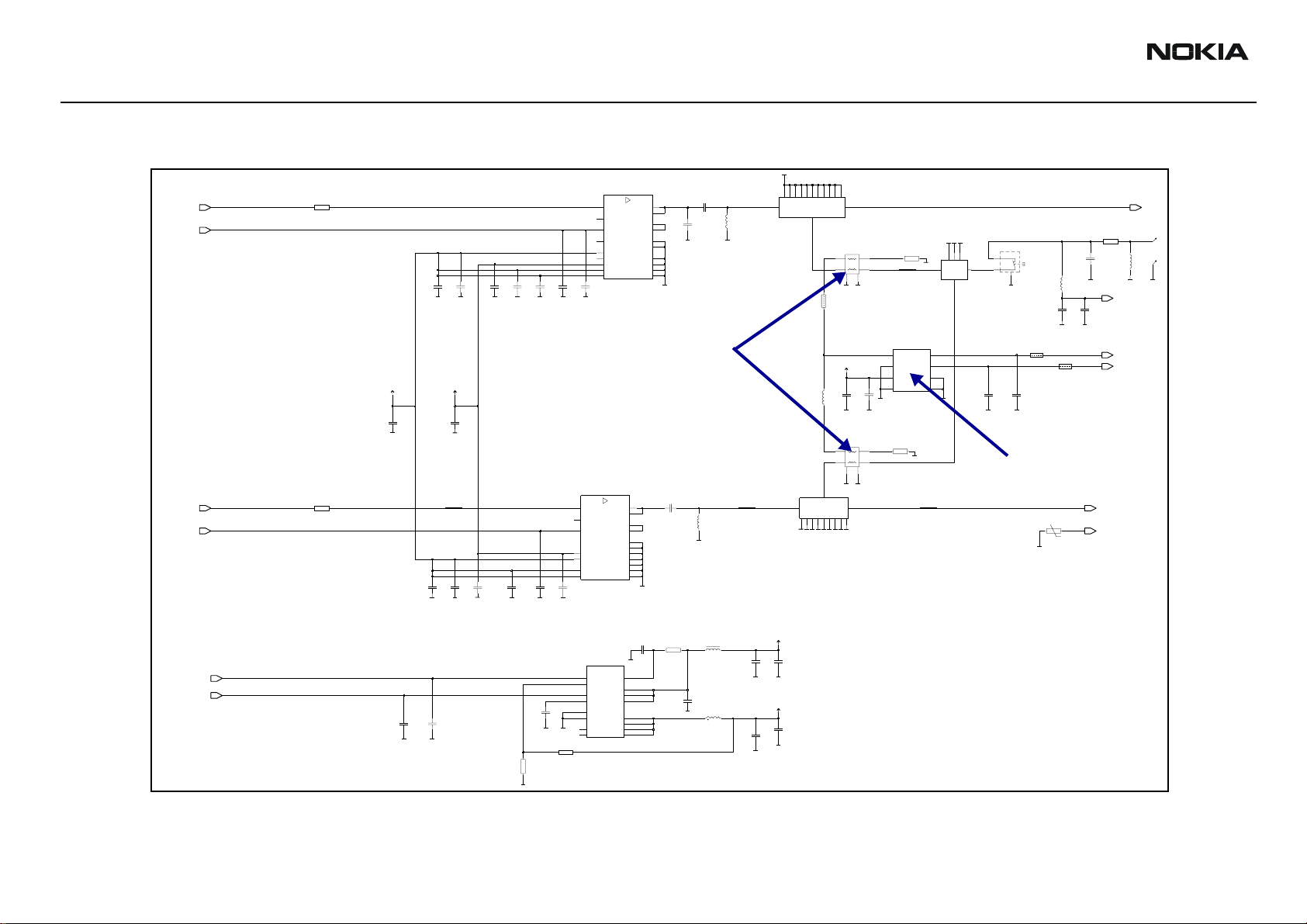
Transmitter RF Troubleshooting
Following is the block diagram for the Tx RF system.
Figure 3: Transmitter system block diagram
Page 8 Company Confidential Issue 1 - September 2006
Page 9
6275/6275i (RM-154)
S
Nokia Customer Care RF Description and Troubleshooting
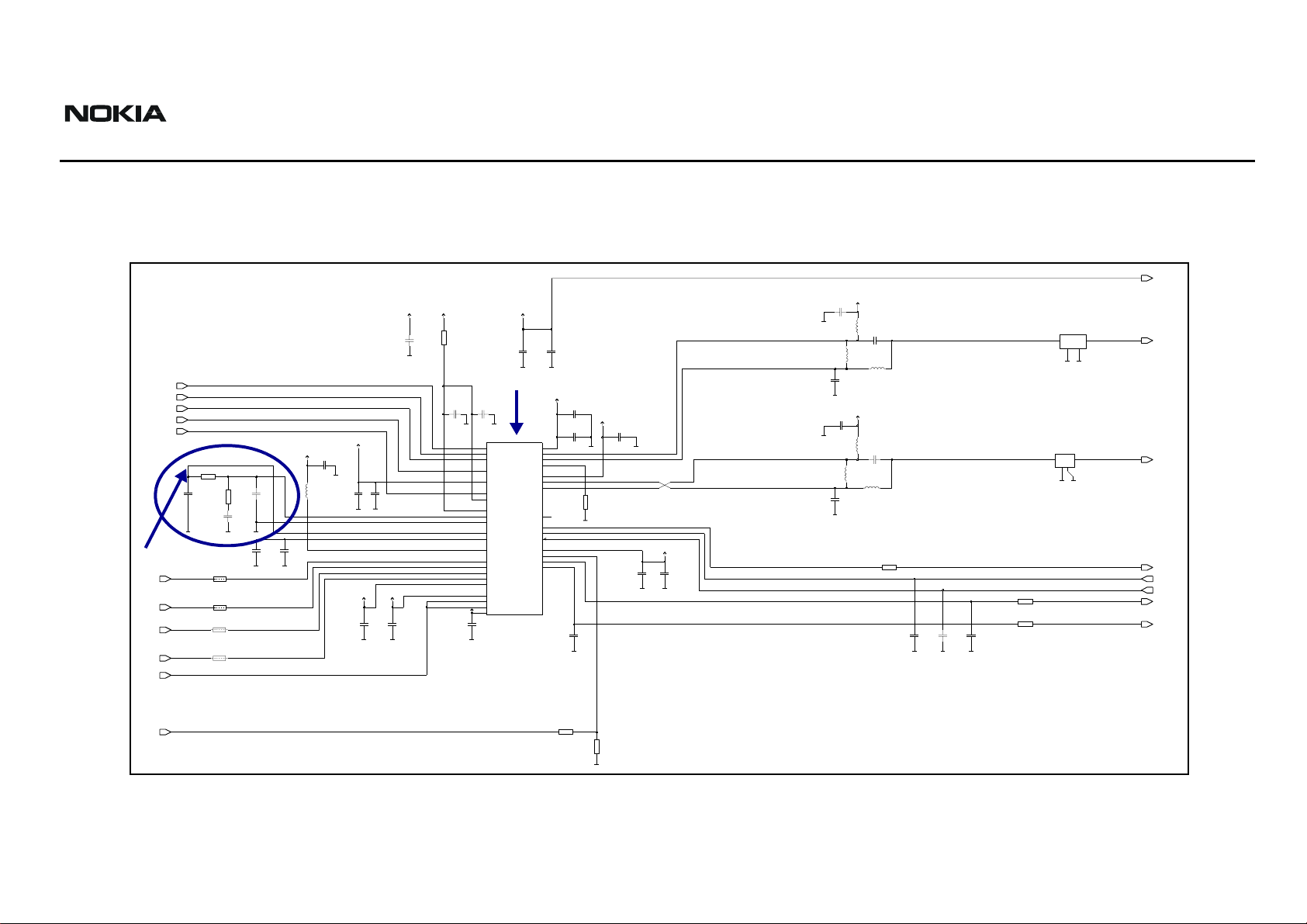
Transmitter Schematics
The following schematics are for general reference only. See the Schematics chapter for detailed versions.
FALSE_DET
VR2
C7022
GND
C7024
GND
C7027
3p3
L7001
27nH
C7023
1p2
L7002
33nH
L7003
1p2
0p5
27nH
GND
VR2
C7025
L7004
6n8H
C7026
0p5
L7005
12nH
L7006
6n8H
GND
R7010
0R
R7011
150R
R7012
C7029
C7031
C7030
3p3
GND
30p
3p3
GND
GND
180R
Z7000
B39841-B9003-E910
836.5MHz
OUT
IN
GND
GND
GND
Cell TX filter
Z7001
B39192-B9014-E910
1850-1910MHz
IN
OUT
GND
GND
GND
PCS TX filter
PA_INPUT_CEL
PA_INPUT_PC
PWROUT
TEMP
DCOUT
IREF_CEL
IREF_PCS
RF_BUS_ENABLE
RF_BUS_DATA
RF_BUS_CLK
TX_GATE
F_REF_TX
Loop filter
R7001
10k
C7005
R7002
100p
27k
C7006
2n2
GND
TX LO lock voltage
TX_IP
TX_IN
TX_QP
TX_QN
TX_AGC1
R7003
SHORT_CIRCUIT
R7004
SHORT_CIRCUIT
R7005
SHORT_CIRCUIT
R7006
SHORT_CIRCUIT
VR6
VR6
C7000
R7000
0R
10n
GND
C7003
3p3
C7015
GND
VR2
33p
GND
VIO
C7010
VR6
3p3
GND
C7007
100p
GND
GND
C7009
C7008
1u0
4p7
GND
GND
C7011
10n
C7013
C7012
18p
GND
GND
VIO
VR2
C7014
18p
33p
GND
GND
L7000
27nH
TX IC
C7004
220p
GND
JUPITER_D4_PMB3365G
31
ENABLE
32
DATA
33
CLOCK
34
TX_GATE
35
VDD_BUS
36
FREF
37
VDD_PLL
38
VDD_CP
39
CP
1
GND_CP
2
VTUNE
3
VCC_VCO30PDET_IN
4
VCC_LO5VCC_PA(4.75V)
9
BBI
10
BBIX
11
BBQ
12
BBQX
14
VCC_MOD
15
AGC_REF
16
AGC1
17
AGC2
18
VCC_RF
BOTTOM PLATE=
C7001
N7000
VR2
10n
GND
VCC_CDRV
ISET_DRV
VCC_PDRV
PDET_OUT
PDET_REF
COUTX
POUTX
ISET_PA
C7002
100n
GND
VR2
C7016
10n
VR2
C7018
C7017
20
22
COUT
23
19
27
24
25
POUT
R7009
21
NC
PWROUT_1
28
TEMP
29
DCOUT
6
7
IPA1
8
IPA2
GND
C7019
12p
10p
47p
GND
GND
12k
GND
VR1B
C7021
C7020
10n
18p
GND
GND
GND
PA_BIAS
R7007
22k
R7008
43k
GND
Figure 4: Transmitter schematic 1
Issue 1 - September 2006 Company Confidential Page 9
Page 10
6275/6275i (RM-154)
BLACKCOMB
RF Description and Troubleshooting Nokia Customer Care
GND
PCS PA
N7300
PA_INPUT_PCS LNA_PCS
IREF_PCS
R7300
0R
C7304
C7303
C7305
C7301
C7300
1n0
GND
C7302
3p3
10n
GND
GND
3p3
GND
C7306
1n015p
GND
GND
RF3448E5
5
RFin
RFout
RFout
1
Vid
NA(CX2)
23
NA(CX2)
Iref/Vref
6
NA
GND/NC
GND/NC
7
Vcc1
89
Vcc1
GND
24
Vcc1
GND
13
GND
Vcc2
Vcc220GND
GND
BOT_SURF=
10p
GND
PCS
C7326
3p3
15
16
C7307
3
4
2
18
14
17
22
GND
L7301
3n9H
NA
GND
GND
Couplers
VBAT
C7318
10U
GND
C7321
C7320
C7319
6n8
270p 1n0
GND
C7322
1n0
1n0
GND
GND
GND
C7323
Cell PA
N7301
RF3449E4
3
RFout
RFin
RFout
6
Vid
24
Iref
GND/NC
GND/NC
1
Vbias
7
Vcc18GND
12
Vcc2
18
Vcc2
C7324
3p3
GND
GND
BOT_SURF=
CELL
GND
C7325
7p5
15
16
20
NC
21
NC
4
13
2
GND
14
GND
17
GND
23
GND
L7306
22nH
GND
GND
PA_INPUT_CEL
IREF_CEL
R7306
VCC_PA
C7317
10U
GND
0R
PCS duplexer
Z7300
DUPLEX
TX
FILTER
R7302
SHORT_CIRCUIT
Z7302
TX RX
GND
Cell duplexer
PCS
RX
ANT
GND
GND
L7302
EHF4CM1880
6
DOUT 4
ROUT
1
IN 3
OUT
GND
GND
GND
GND
STPAC01F2
C3
RFIn
C2
C7314
GND
Gnd1
C1
Bias
B3
Gnd1
10p
GND
GND
R7307
ROUT
6
56R
OUT
1
GND
2
VR2
C7313
L7304
10nH
10n
GND
L7305
EHF4CM0836A
DOUT
4
IN
3
GND
5
GND
ANT
DUPLEX
FILTER
GND
GND
GND
GND
GND
GND
GND
GND
R7301
N7302
GND
Z7301
2
4
6
GND
56R
3
DIPLEXER
P1
P2
1
A2
VTemp
A3
DCout
B1
Gnd2
B2
Gnd1
GND
GND
X7300
In R2
5
In C1
P3
GND
SHORT_CIRCUIT
C7315
C7316
3n3
3n3
GND
GND
Power detector
R7304
GND
L7303
33nH
C7311
10p
GND
R7305
SHORT_CIRCUIT
R7308
47k
C7312
C7370
47p
NA
GND
47p
GND
R7310
0R
LNA_CEL
PA_TEMP
L7397
10nH
ANT_SENSE
TEMP
DCOUT
TP7300
TP7301
GND
GND
C7358
VBAT
C7356
C7357
10n
10U
GND
GND
VCC_PA
C7353
47p
10U
GND
GND
PA_DC_DC_PDM
PA_DC_DC_ENABLE
C7350
C7354
4u7
N7350
RF4013E2.2
GND
U//U
16
2
VRCVSET
5
VSENS
15
VBAT
14
3
VBAT
EN
4
13
CF
C7352
R7351
10p
GND
GND
R7352
8k2
NA
1k8
GND
C7351
47p
47p
GND
GND
6
GND
7
GND
1
NC10VOUT
8
NC VOUT
17=GND
VBAT
12
VOUT
11
VOUT
9
R7350
L7350
42R/100MHz
100R
C7355
L7351
4u7
1u5H
GND
Figure 5: Transmitter schematic 2
Page 10 Company Confidential Issue 1 - September 2006
Page 11

6275/6275i (RM-154)
Nokia Customer Care RF Description and Troubleshooting
Transmitter Troubleshooting Guidelines
Use the following guidelines when troubleshooting.
• Always perform visual inspection of PCB under microscope to check proper
placement, rotation, and soldering of components.
• Look for the presence of a well-defined CDMA modulated signal on a spectrum
analyzer at the correct frequency. If a signal is present but off frequency or the
shape looks distorted, check the synthesizer. Possibly, one of the synthesizers is
not locked or the VCO has no output signal. Check the synthesizers for proper
frequency and amplitude. See "Tx Output Spectrum" on page 18 and "Synthesizer
Troubleshooting"onpage33.
• Check that power supplies to the transmitter have the correct voltage. See "Tx RF
Component Diagram" on page 19.
• If the signal is very low in amplitude, check the probing diagram to determine
what part of the TX chain is ‘broken’. See "DC Test Points" on page 20.
• Check that AGC PDMs produce and adjust TX power within the proper limits.
Transmitter Troubleshooting Setup
Use the following sets of procedures to troubleshoot the transmitter using Phoenix.
1. Tx power at the RF connector.
2. All Tx DC points.
3. All soldering jig points for the whole Tx chain.
4. UHF LO presence:
• If the UHF LO is present, check the N7000 output.
• If the UHF LO is not present, it is a synthesizer problem.
5. If there is no N7000 output:
a. Change the N7000.
b. If the problem persists, reflow the duplexers, diplexer, and couplers.
c. If the problem persists, change the PA.
6. If there are several failed mobile terminals with the same symptoms, it may be
necessary to break one to determine the cause.
Use the following sections to set up troubleshooting in Phoenix according to the band
you are using:
•"AMPS Tx Setup"onpage12
•"Cell Tx Setup"onpage13
•"PCS Setup"onpage15
Issue 1 - September 2006 Company Confidential Page 11
Page 12
6275/6275i (RM-154)
RF Description and Troubleshooting
AMPS Tx Setup
Use the following procedures to prepare for AMPS Tx troubleshooting using Phoenix.
Note the 6236i variant does not support AMPS.
1. Connect the RF test connector to a spectrum analyzer.
2. Connect the mobile terminal to the PC via a test jig. (The bottom connector is a
USB port.)
3. Connect a power supply to the mobile terminal.
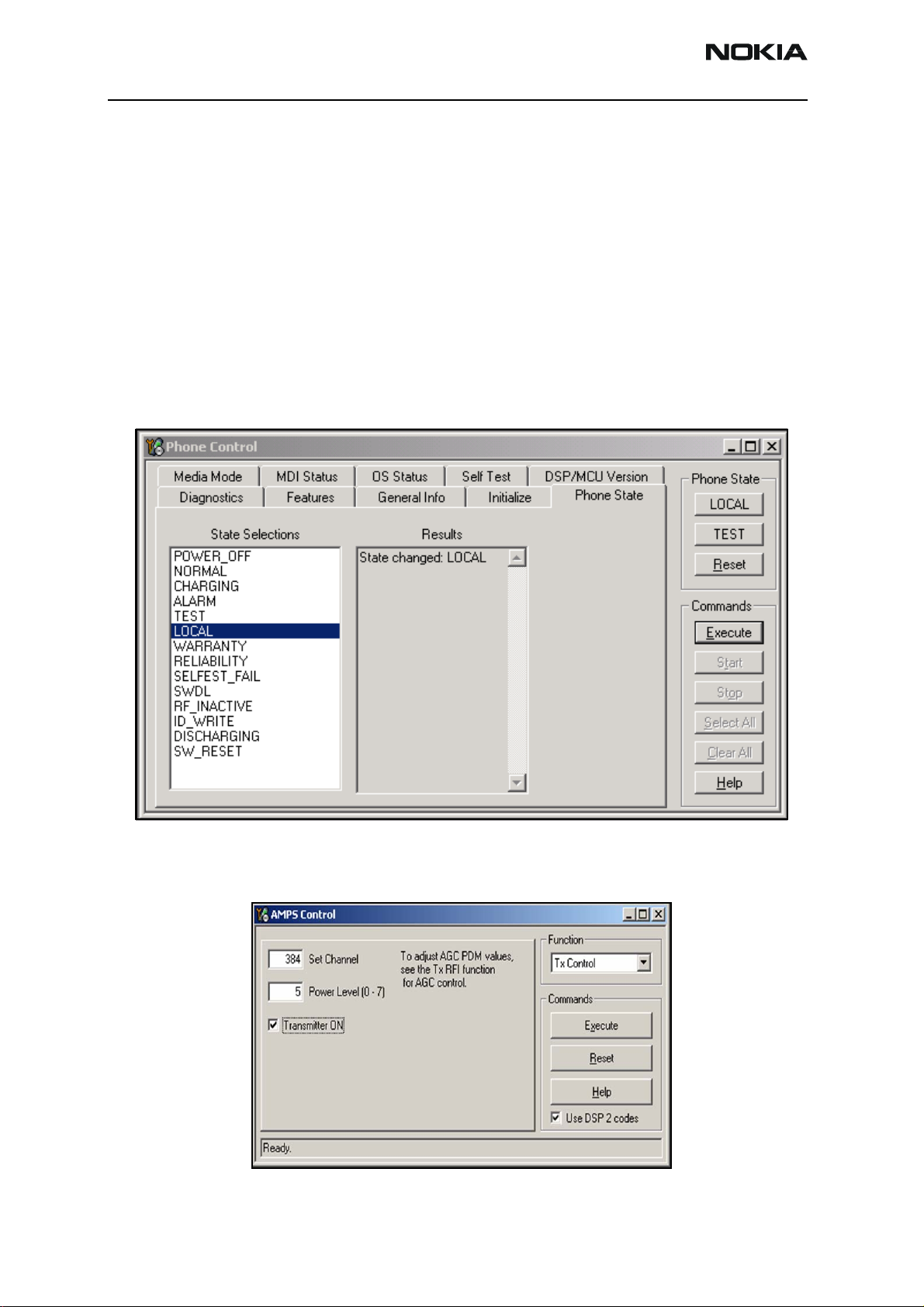
4. Open the Troubleshooting menu, and click Phone Control. The Phone Control
dialog box appears.
5. Click the LOCAL button in the Phone State tab to put the mobile terminal into
Local Mode.
Figure 6: Phone Control dialog box
6. Open the Troubleshooting menu, point to AMPS, and click AMPS Control. The
AMPS Control dialog box appears.
Page 12 Company Confidential Issue 1 - September 2006
Page 13
6275/6275i (RM-154)
Nokia Customer Care RF Description and Troubleshooting
Figure 7: AMPS Control dialog box
7. In the Function field, select Tx Control.
8. In the Set Channel field, type 384.
9. In the Power Level field, type 5.
10. Select the Transmitter ON and Use DSP 2 codes options.
11. Click Execute.
12. Configure the spectrum analyzer using the following values:
• Center Frequency = 836.52 MHz
• Span = 100 MHz
• Amplitude = 20 dBm
• Attenuation = Auto
• BW = Auto
Cell Tx Setup
Use the following procedures to prepare for Cell Tx troubleshooting using Phoenix.
1. Connect an RF test connector to a call box.
2. Connect the mobile terminal to the PC via a test jig. (The bottom connector is a
3. Connect a power supply to the mobile terminal.
4. On the Phone Control dialog box, click the LOCAL button in the Phone State
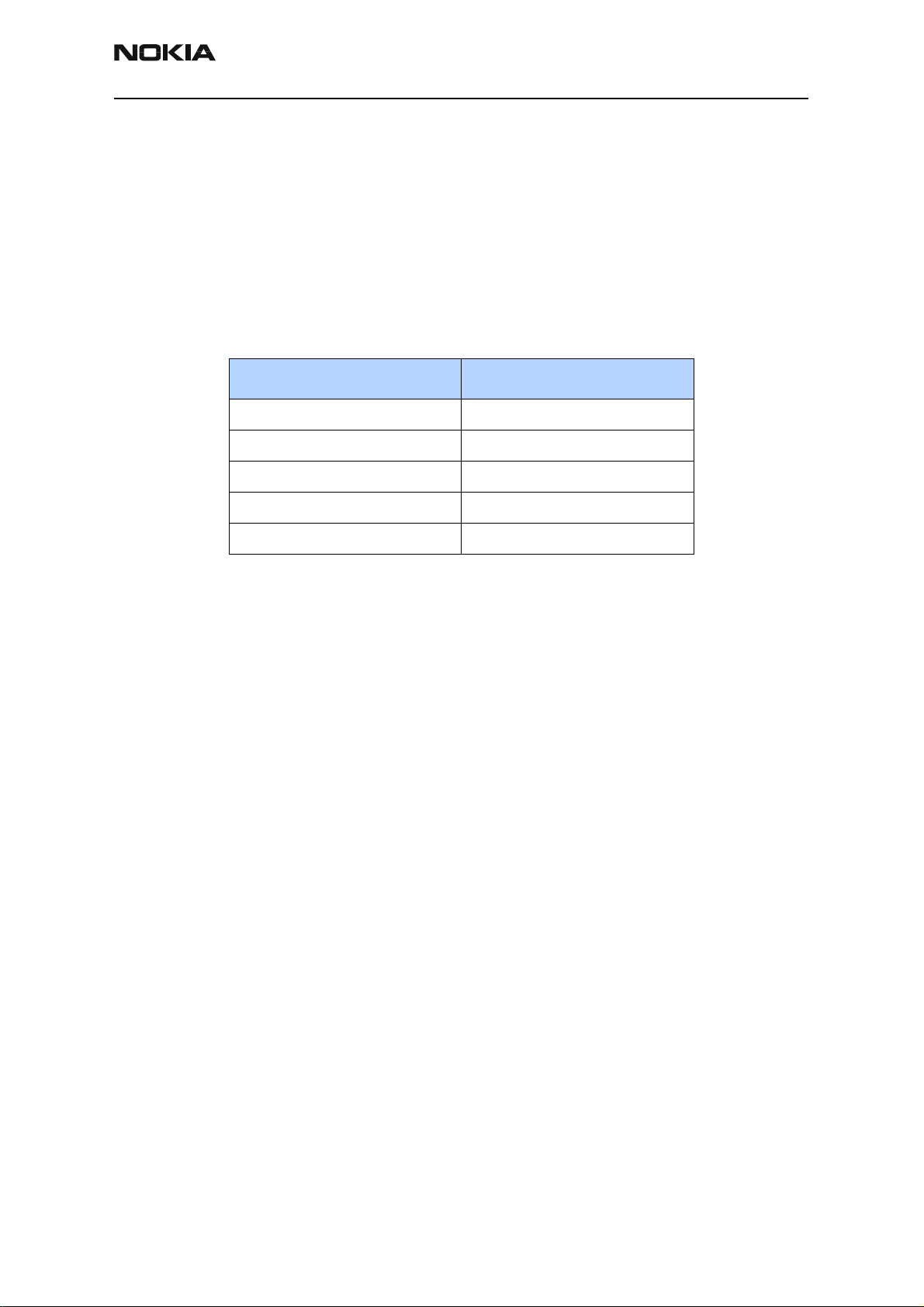
Table 1: RF PDM Values at Power Level 5
Description/Field Reference Value
AGC1 -512
PA_Bias 129
PA_DC_DC 197
USB port.)
area to put the mobile terminal into Local Mode. (See Figure 6 on page 12.)
Issue 1 - September 2006 Company Confidential Page 13
Page 14
6275/6275i (RM-154)
RF Description and Troubleshooting
5. Open the Troubleshooting menu, point to RF, and click RF Main Mode. The RF
Main Mode dialog box appears.
Figure 8: RF Main Mode dialog box for Cell Mode
6. Select the following values on the RF Main Mode dialog box:
• Band = Cell (CDMA)
• Channel = 384
• Mode = Rx/Tx
7. Click Set.
Note: Be sure that the “RF Main Mode set successfully” message appears in
the status bar.
8. Open the Troubleshooting menu, point to RF, and click CDMA Control. The
CDMA Control dialog box appears.
Do NOT select this option
Figure 9: CDMA Control dialog box for Cell Tx troubleshooting
9. Select the following values:
• State = Rho ON
• Band = Cell
• Radio Configuration = Mode 1: IS-95 Voice
Note: Do NOT select the Set default PDM values option.
10. Click Execute.
Page 14 Company Confidential Issue 1 - September 2006
Page 15
6275/6275i (RM-154)
Nokia Customer Care RF Description and Troubleshooting
11. Configure the spectrum analyzer using the following values:
• Center Frequency = 836.52 MHz
• Span = 100 MHz
• Amplitude = 20 dBm
• Attenuation = Auto
• BW = Auto
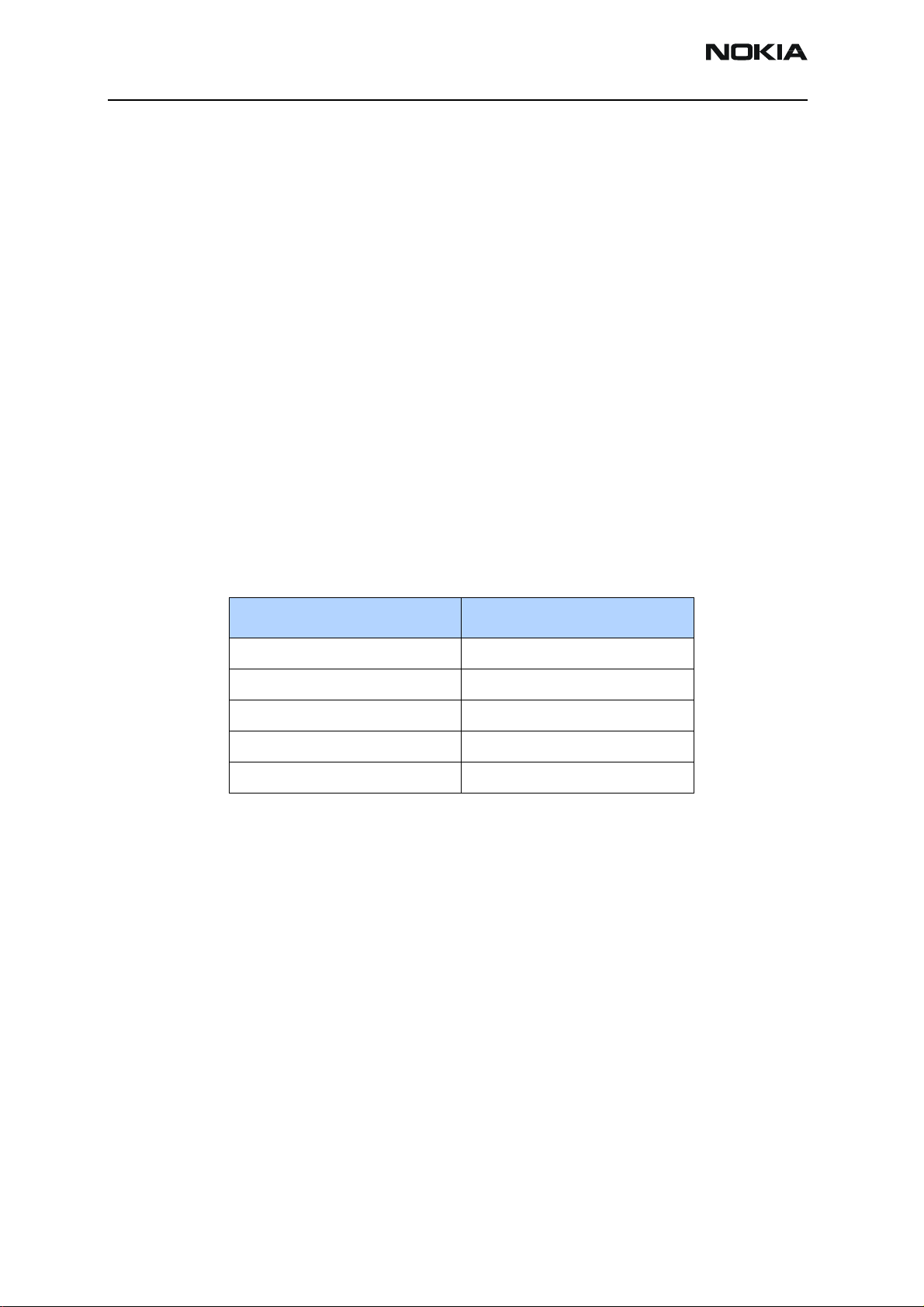
Table 2: RF PDM Values
Description/Field Reference Value
AGC1 -130
PA_Bias 85
PA_DC_DC 110
Pout 16dBm
PCS Setup
Use the following procedures to prepare for PCS Tx troubleshooting using Phoenix.
Current 340mA
1. Connect an RF test connector to a call box.
2. Connect the mobile terminal to the PC via a test jig. (The bottom connector is a
USB port.)
3. Connect a power supply to the mobile terminal.
4. Open the Troubleshooting menu, and point to Phone Control. The Phone
Control dialog box appears. (See Figure 6 on page 12.)
5. Click the LOCAL button in the Phone State area to put the mobile terminal into
Local Mode.
6. Open the Troubleshooting menu, point to RF, and click RF Main Mode. The RF
Main Mode dialog box appears. (See Figure 8 on page 14.)
7. Select the following values on the RF Main Mode dialog box:
• Band = PCS (CDMA)
• Channel = 600
• Mode = Rx/Tx
8. Click Set.
Note: Be sure that the “RF Main Mode set successfully” message appears in
the status bar.
9. Open the Troubleshooting menu, point to RF, and click CDMA Control. The
CDMA Control dialog box appears. (See Figure 9 on page 14.)
Issue 1 - September 2006 Company Confidential Page 15
Page 16
6275/6275i (RM-154)
RF Description and Troubleshooting
10. Select the following values on the CDMA Control dialog box.
• State = Rho ON
• Band = PCS
• Radio Configuration = Mode 1: IS-95 Voice
Note: Do NOT select the “Set default PDM values” option.
11. Click Execute.
12. Open the Troubleshooting menu, point to RF, and click PDM Control.
13. Configure the spectrum analyzer using the following values:
• Center Frequency = 1880 MHz
• Span = 100 MHz
• Amplitude = 20 dBm
• Attenuation = Auto
• BW = Auto
Table 3: RF PDM Values
Description/Field Reference Value
AGC1 -130
PA_Bias 85
PA_DC_DC 110
Pout at RF connector +15dBm
Current 340mA
Transmitter RF Troubleshooting Procedures
After Phoenix is set up using either the AMPS, Cell, or PCS setup procedures, use the
following steps to troubleshoot the transmitter.
1. Using a voltmeter, check to see that all VR2, VR6, and VR1B are on the transmit
system. (See "Tx RF Component Diagram"on page19.)
• If any are missing, look for SMD problems around the Tx IC and the UEMEK.
• If SMD is good, replace the UEMEK.
2. After all DC voltages are present, check the AGC control voltages. (See "AMPS Tx
Setup"onpage12, "Cell Tx Setup"onpage13, or "PCS Setup"onpage15.)
• If the voltages are incorrect, check the SMD around TX_AGC1.
• If the SMDs are correct, replace the D2800.
Page 16 Company Confidential Issue 1 - September 2006
Page 17

6275/6275i (RM-154)
Nokia Customer Care RF Description and Troubleshooting
3. Using an oscilloscope, check the I and Q input modulation wave forms at test
points. See "Tx RF Components of the PWB"onpage19. They should all be
present with an AC swing of about 500mVpp, with an offset of +1.2V.
• If one or more waveforms is missing, look for SMD problems around these
resistors.
• If the SMD is good, replace the UEMEK.
4. Use an AAS-10 RF probe to probe the Cell Tx output of the Tx IC.
• If there is no RF or low RF, look for a faulty SMD around the Tx IC.
• If the SMD is okay, replace the N7000.
5. Probe the PA input.
• If the level is low, look for an SMD issue on the Tx filter.
• Reflow or replace the filter as necessary.
6. Probe the PA output.
• If the RF is missing or low, look for Vbatt voltages and SMD issues on and
around the PA.
• If these are okay, replace the PA.
7. Probe the duplexer output.
• If the RF is missing or low, reflow or replace the duplexer.
8. Probe the coupler output.
• If the RF is missing or low, reflow or replace the coupler.
9. Probe the diplexer output.
• If the RF is missing or low, reflow or replace the diplexer.
Failed Test: Tx PA Detector
Use the following steps if you encounter a failed test for the Tx PA detector:
10. Use Phoenix to set the mobile terminal into Local Mode and activate the Tx with
default output power.
11. The output power at the RF test connector should be 15dBm ± 4dB. If not, adjust
the PDM values or troubleshoot per procedure above.
12. Using a voltmeter on DC, probe the detector output at C7315. The voltmeter
should read approximately 1.7V. If not, replace N7302.
Issue 1 - September 2006 Company Confidential Page 17
Page 18
6275/6275i (RM-154)
RF Description and Troubleshooting
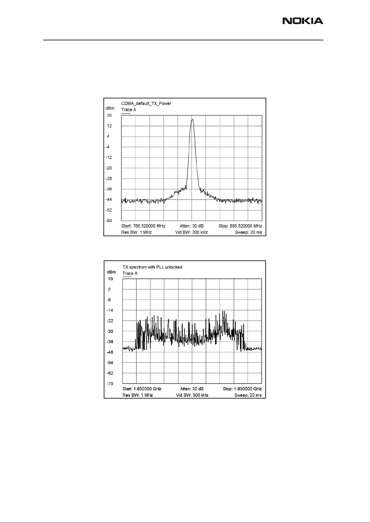
Tx Output Spectrum
Following is the correct output of the mobile terminal on a spectrum analyzer with
100MHz span. Note that if you are using the AAS-10 probe with the mobile terminal
connected to the call box, the amplitude should be approximately -7dBm at the antenna
test point on the top of the PWB.
Figure 10: Correct output spectrum
Following is an example of incorrect output.
Figure 11: Incorrect output spectrum
Page 18 Company Confidential Issue 1 - September 2006
Page 19
6275/6275i (RM-154)
Nokia Customer Care RF Description and Troubleshooting
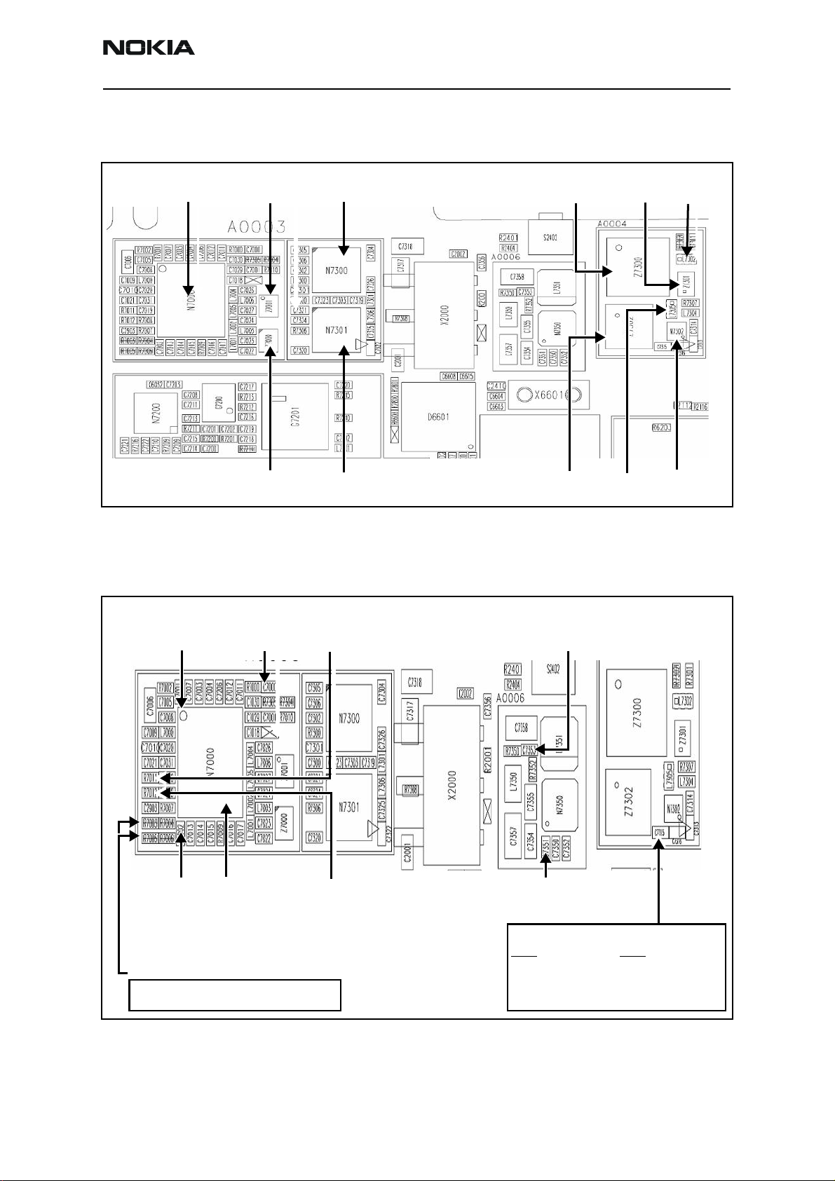
Tx RF Component Diagram
Following are the Tx RF components.
Tx IC
Tx DC Probe Points
Following are the Tx DC probe points of the PWB.
Tx UHF LO
Lock Voltage
1.2V
PCS Tx
SAW filter
Cell Tx
SAW Filter
VR6: VCC_PA:
2.8V 0-4.6V
PCS PA
Cell PA
Figure 12: Tx RF Components of the PWB
Iref_Cell:
~2.4-3.4V
Duplexer
Cell
Duplexer Detector
PCS
Diplexer
Cell
Coupler
PCS
Coupler
Power
I
Q
VR2:
2.76V
Tx IQ inputs
approx. 1.2 V
approx. 500 mV p-p (with O’scope)
AGC 1
Pin 16
0.1 to1.8V
Iref_Pcs:
2.3-2.9 V
Figure 13: Tx DC probe points
PA_DC_DC_PDM:
0-1.9 V
Power Detector Output (DCOUT)
PCS:
2.0V @ <5dBm
1.7V @ <15dBm
1.2V @ <23dBm
Cell:
2.0 V @ <5dBm
1.8 V @ <15dBm
1.4 V @ <23dBm
Issue 1 - September 2006 Company Confidential Page 19
Page 20
6275/6275i (RM-154)
RF Description and Troubleshooting
Tx RF Probe Points
Figure 14 shows the Tx RF probe points of the PWB.
PCS Frequency 1880 MHz
PCS TX IC out:
-7 dBm -13 dBm +17 dBm
PCS PA in:
PCS PA out:
PCS Duplexer
out: +15 dBm
Diplexer out:
PCS +16 dBm
Cell +10 dBm
Amps +1 dBm
PCS PDM:
PA_DC_DC = 110
PA_Bias = 85
AGC1 = -130
Amps PDM:
PA_DC_DC = 197
PA_Bias = 129
AGC1 = -512
Pwr Detector in
PCS: -13 dBm
Cell: +4 dBm
Amps: -20 dBm
Cell TX IC out: -7 dBm
Amps -33 dBm
Cell, Amps Frequency 836.25 MHz
Cell PA in: -7 dBm
Amps -33 dBm
DC Test Points
Figure 15 shows the DC test points.
Vbatt 3.2 to 4.7 V
VR1B: 4.75 V (TX)
VR1A: 4.75 V (Synth)
VR2: 2.78 V (TX)
VR4: 2.78 V (RX)
VR7: 2.78 V (RX)
Cell PA out: +20 dBm
Amps -6 dBm
Figure 14: Tx RF probe points
VR6: Rx 2.78 V (TX)
Cell Duplexer out:
+20 dBm
Amps -7 dBm
VR5: Rx 2.78 V (RX)
Cell PDM:
PA_DC_DC = 110
PA_Bias = 85
AGC1 = -130
VIO 1.8 V
VR3: 2.78 V (Synth)
Figure 15: DC Test Points
Receiver RF Troubleshooting
The heart of the receiver is the Rx Front-end IC, which contains two LNAs and mixers.
The other components are passive. There are two RF SAW filters for the Cell and PCS
bands. In addition, there are two IF filters, an IF SAW for CDMA and an IF Crystal for
AMPS.
Page 20 Company Confidential Issue 1 - September 2006
Page 21

6275/6275i (RM-154)
Nokia Customer Care RF Description and Troubleshooting
Receiver Block Diagram
Following is the Rx System block diagram.
Figure 16: Receiver System block diagram
Issue 1 - September 2006 Company Confidential Page 21
Page 22

6275/6275i (RM-154)
D
D
RF Description and Troubleshooting Nokia Customer Care
Receiver Schematics
The following schematics are for general reference only. See the Schematics chapter for detailed versions.
LNA_PCS
LNA_CEL
BAND_SEL_FE
GAIN_CTL
IF_SEL
PCS_CELL_LO
Vrx
SHORT_CIRCUIT
R7161
47k
R7162
47k
R7163
47k
R7160
C7189
C7161
C7162
100p
C7163
100p
C7164
100p
VR5
Vrx
C7165
L7165
12nH
56p
GND
L7166
3n3H
C7173
R7164
4R3
C7169
1p5
L7168
18nH
C7174
3n3
GND
12p
GND
C7167
12p
GND
L7160
0p5
7n5H
RX front end IC
L7161
GND
19n0H
GND
GND
GND
GND
L7163
3n3H
L7162
12nH
GND
L7164
82nH
GND
N7160
SC-7195-C
4 Pmix_in
16 Cmix_in 17Mix_out
11
3
7
18
19
23
24
Plna_in10
Clna_in
Band_sel
Gain_cntl
IFA_In
IFA_src
IF_Sel
LO_in
Plna_out 8
Clna_out
CDMA_out 22
C7172
20AMPS_out
13
2
Vdd
1
Vdd
5
Vdd
14
Vdd
15
Vdd
6
GND
9
GND
12
GND
GND
L7169
Vrx
15nH
47n
GND
R7166
4R3
Cell RF SAW filter
C7166
1p8
Vrx
C7168
100n
GND
L7167
220nH
C7171
5p6
VR4
R7165
82R
C7175
22p
GND
Z7160
881.52MHz
IN GND OUT
PCS RF SAW filter
Z7161
1960MHz
IN
OUT
GND
C7170
100p
L7170
82nH
L7176
120nH
C7184
C7177
C7182
2p2
C7176
1n0
4p7
3n3
GND
Z7162
128VH30A
L7171
180nH
C7178
Vrx
C7183
100n
GND
GND
C7185
100p
128.1MHz
OUT
IN
GND
3p9
AMPS IF SAW filter
GND
CDMA IF SAW filter
GND
Z7163
B39131-B4959-H310
128.1MHz
In
Bal_Out
Bal_Out
/Gnd
GND
AMPS
L7172
120nH
C7179
10p
L7177
100nH
L7173
120nH
GND
GND
C7180
L7175
220nH
6p8
L7174
220nH
C7181
GND
6p8
C7187
12p
C7188
12p
L7178
120nH
L7179
120nH
GND
C
C
Figure 17: Receiver schematics - 1 Rx Front-end
Page 22 Company Confidential Issue 1 - September 2006
Page 23

6275/6275i (RM-154)
Nokia Customer Care RF Description and Troubleshooting
F_REF_RX
VHF Loop Filter
4k7
BBY57-02W
R7100
C7101
1k0
C7103
33p
V7100
L7101
33nH
VIO
R7103
8k2
C7105
10n
R7101
C7102
330n
33n
470R
C7104
1n0
R7104
VR5
E3
K8
F1
E1
A1
B1
VR5
A2
A3
VR7
C2
C1
VR7
J9
H10
C10
B10
A9
A10
D8
A8
A5
B6
B5
E10
F9
D9
D10
G2
G1
27k
N7100
BATMAND_PBFREE
VCC_CH
CLK19M2
PD_LO2
RESO_LO2
RX_VHFBUF_p
RX_VHFBUF_n
VCC_LO
GND_LO
VCC_PLL2
VSS_PLL2
VCC_ext
VSS_ext
RX_IF_p
RX_IF_n
RX_IF1_n
RX_IF1_p
VCC4
GND4
VCC8
GND8a
GND8b
AGC_Ref
RX_IF_AGC
VCC5
GND5
Rbias
Vref
TEST_OUT
GND_CH
RFBusClk
RFBusEn1X
VCO_ctrl
LPB_SW
VCC6
GND6
VCC_DIGI
VSS_DIGI
Reset
RFBusData
OUT1
OUT2
OUT3
OUT4
OUT5
OUT6
VCC_CTRL
GND_CTRL
VCC_bias
GND_bias
RX_IP
RX_IN
RX_QP
RX_QN
IFI_TEST_p
IFI_TEST_n
IFQ_TEST_P
IFQ_TEST_n
GND_IF
VCC_IF
VDD9
VSS9
OFFQ
OFFI
B2
D2
K7
H5
J10
K10
VR5
C3
D1
K9
K6
J5
J6
H9
H8
G8
F10
A7
A6
B7
B8
F2
H1
J1
H2
K1
K2
E8
E9
G9
G10
A4
B4
J3
K3
K5
K4
VIO
BATM01
VR7
VR5
VR5
VR5
RF_BUS_CLK
RF_BUS_ENABLE
BAND_SEL_FE
PURX
RF_BUS_DATA
BAND_SEL_VCO
GAIN_CTL
IF_SEL
RX_IP
RX_IN
RX_QP
RX_QN
C7100
10n
R7102
Rx VHF Lo Lock Voltage
1.2-1.7 VDC
CDMA_IF_P
CDMA_IF_N
AMPS_IF_N
AMPS_IF_P
RX_IF_AGC
VREF
C7106
10n
Figure 18: Receiver schematic - 2 Rx Back-end
Issue 1 - September 2006 Company Confidential Page 23
Page 24

6275/6275i (RM-154)
RF Description and Troubleshooting
RF AGC Status
When configuring the values on the RF AGC Status dialog box, note the following:
• The RF AGC status functionality only works in Call Mode.
•In the PLL Lock Status area, bright green indicates a locked PLL and dark green
indicates an unlocked PLL.
• Clicking the Update Now button updates the screen once.
• Clicking the Auto Update button updates the screen every second continuously.
Note: RF AGC Status works only in Call Mode.
RSSI
Tx Power
AFC PDM
LNA Gain
(High (Red)/Low)
PA AGC PA_DC_DC
PDM PDM
Rx IF AGC PDM
Tx AGC1
PDM
Bright Green indicates Locked PLL
Dark Green indicates Locked PLL
Updates
when clicked
once every second
Updates
continuously
Figure 19: RF AGC Status dialog box
Page 24 Company Confidential Issue 1 - September 2006
Page 25

6275/6275i (RM-154)
Nokia Customer Care RF Description and Troubleshooting
Turning on the Rx Path
Use the following steps to turn on the Rx path using Phoenix.
1. On the Phone Control dialog box, click the LOCAL button in the Phone State
area to put the mobile terminal into Local Mode.
Figure 20: Phone Control dialog box
2. Click the Execute button.
3. Depending on the band, use the applicable settings from the table below on the
RF Main Mode dialog box.
Table 4: RF Main Mode Dialog Box Settings
Band Mode Channel
AMPS Rx = 881.52 MHz 384
Cell Rx = 881.52 MHz 384
PCS Rx = 1960 MHz 600
Issue 1 - September 2006 Company Confidential Page 25
Page 26

6275/6275i (RM-154)
RF Description and Troubleshooting
AMPS
Cell
PCS
Figure 21: RF Main Mode dialog boxes for AMPS, Cell, and PCS
Page 26 Company Confidential Issue 1 - September 2006
Page 27

6275/6275i (RM-154)
Nokia Customer Care RF Description and Troubleshooting
Switching the Rx Gain States
Use the RF Gen I/O dialog box to switch the gain state (Hi and Lo) for CDMA and AMPS
modes.
Hi Gain (Default)
State at power up
Low Gain State
Cell
AMPS
PCS
CDMA
Figure 22: RF Gen I/O dialog box
Receiver Diagnostic Signal Tracing
Use the following to trace the receiver signal.
• An RF signal generator is recommended, however an Agilent call box 8960 may
also be used. For 8960, hit Button CALL SETUP, soft button Active Cell, and then
select CW.
• Inject a CW signal for PCS (1960MHz) or Cell/AMPS (881.52MHz) at a fixed –
25dBm power level.
• Take measurements with the AAS-10 probe.
• Signal levels are approximate, and accuracy may be ± 2dB or more, depending on
position and grounding of probe.
Issue 1 - September 2006 Company Confidential Page 27
Page 28

6275/6275i (RM-154)
RF Description and Troubleshooting
Receiver RF Probe Points
7
IFA_in (to RX FE RFIC)
128.1 MHz @ -15 dBm (HG)
128.1 MHz @-32 dBm (LG)
3
Cell CH384 (to RF SAW)
881.52MHz @ -20 dBm (HG)
881.52MHz @ -36 dBm (LG)
6
IF MIX OUT (from RX FE IC)
128.1MHz @ -20 dBm (HG)
128.1MHz @ -37 dBm (LG)
1
RX UHF LO (from VCO)
Cell: 1009.62MHz @ -8 dBm
PCS: 2088.1MHz @ -14 dBm
AMPS IF
crystal filter
CDMA IF
SAW filter
Cell RF
SAW filter
RX Front End IC
PCS RF
SAW filter
Figure 23: Receiver RF Probe points
4
Cell CH384 (from Duplexer)
881.52MHz @ -31 dBm
2
PCS CH600 (from Duplexer)
1960MHz @ -40 dBm
5
PCS CH600 (to RF SAW)
1960MHz @ -30 dBm (HG)
1960MHz @ -45 dBm (LG)
Page 28 Company Confidential Issue 1 - September 2006
Page 29

6275/6275i (RM-154)
Nokia Customer Care RF Description and Troubleshooting
Receiver IF Probe Points
8
AMPS IF (to MCF) 128.1MHz
CELL CH384 @ -17 dBm (HG)
CELL CH384 @ -34 dBm (LG)
RX UHF Lo
CELL CH384 -8 dBm @
1009.62MHz
PCS CH600 -14 dBm @
2088.1MHz
IF VHF lo 256.2 MHz
-2.5 dBm (when locked)
11
AMPS_IF_P and N (to RX IC) 128.1MHz
CELL -23 dBm (HG) -41 dBm (LG)
9
CDMA_IF_P and N (to RX IC) 128.1MHz
CELL -25 dBm (HG) -40 dBm (LG)
PCS -25 dBm (HG) -40 dBm (LG)
Figure 24: Receiver IF Probe points
10
CDMA IF (to SAW) 128.1MHz
CELL CH384 @ -6 dBm (HG)
CELL CH384 @ -23 dBm (LG)
PCS CH600 @ -6 dBm (HG)
PCS CH600 @ -20 dBm (LG)
Issue 1 - September 2006 Company Confidential Page 29
Page 30

6275/6275i (RM-154)
RF Description and Troubleshooting
Receiver DC Probe Points
RX RF Lo lock voltage 1.2 to 1.7 VDC
LO Vdd = 2.7 VDC LO
Vdd supply lines for
Cell and PCS
VR4 = 2.7 VDC
NOTE: There is no part installed here.
There are only two pads.
RX Front End IC
VIO = 1.8 VDC BE IC
Vdd supply lines for
Cell and PCS
(Vrx) = 2.79 VDC RX FE IC Vdd supply line for CDMA and AMPS IFs
Figure 25: Rx DC test points
Page 30 Company Confidential Issue 1 - September 2006
Page 31

6275/6275i (RM-154)
Nokia Customer Care RF Description and Troubleshooting
Receiver Logic Input Voltages
Measure logic levels for Rx Front-End (N7160). Figure 26 shows the receiver logic input
voltages.
1
Figure 26: Receiver logic input voltage test points
3
2
Table 5 includes the logic levels for the N7160.
Table 5: Rx Front-end (N7160) Logic Levels
Logic Input Voltages
Modes
1
IF_SEL2 BAND3 GAIN_CTL
Cell CDMA High Gain 0 V 0.1 V 2.7 V
Cell CDMA Low Gain 0 V 0.1 V 0 V
PCS CDMA High Gain 0 V 2.7 V 2.7 V
PCS CDMA Low Gain 0 V 2.75 V 0 V
AMPS High Gain 2.7 V 0.1 V 2.7 V
AMPS Low Gain 2.7 V 0.1 V 0 V
If the logic levels are significantly off (± 0.2V), replace the Back-End IC (N7100). If the
levels are still bad, replace the Rx Front-End IC (N7160) and re-measure. If the voltages
are still out of specifications, refer to the Baseband Troubleshooting chapter.
Rx Front-End Receiver Troubleshooting
Keep the following points in mind regarding the Rx Front-end receiver:
• There is a separate LNA for 800MHz (Cell and AMPS) and 1900MHz (PCS).
• There is a separate RFA (inside Rx Front-end IC) for 800MHz (Cell and AMPS) and
1900MHz (PCS).
• After the RFA, there is a mixer, and then the signals are separated by CDMA (Cell
and PCS) and AMPS.
Issue 1 - September 2006 Company Confidential Page 31
Page 32

6275/6275i (RM-154)
RF Description and Troubleshooting
For example, if there is no IF frequency (128.1MHz) check both Cell and PCS. If
only one has 128.1MHz at L7162, ensure that IF_SEL is working. If it is, then
replace the Rx Front-end IC due to a bad RFA.
If Cell and AMPS are working but PCS is not, look at the band select line and the
PCS LNA before replacing the Rx Front-end IC.
N7160
IFAs
Lo
Buffer
Cell
RFA
PCS
RFA
Cell
LNA
PCS
LNA
Figure 27: N7160 receiver
There are two common explanations for a Rx Front-end IC failure consisting of high
current in Local Mode with just the Rx turned on:
• No presence of a LO signal
• Input impedance drop is shorting out one of the DC supply pins to the chip
IMPORTANT: You must check for both conditions before replacing the chip. If you
have no LO signal, refer to "UHF Synthesizer Troubleshooting"onpage41. If you have a
significant supply voltage drop on one of the supply pins, then replace the Rx Front-end
IC.
Table 6: Rx Front-end IC Conditions and Supply Currents
Condition: Local Mode, Set
Rx Only in RF Main Mode
Good mobile terminal 100mA
No UHF LO signal present 254mA
Pin 13 shorted 255mA
Supply Current
(From Power Supply)
Page 32 Company Confidential Issue 1 - September 2006
Page 33

6275/6275i (RM-154)
Nokia Customer Care RF Description and Troubleshooting
Synthesizer Troubleshooting
Faulty synthesizers can cause both Rx and Tx failures during tuning, in addition to the
VCTCXO tuning. However, first check for the presence of various LO signals and their
proper levels. If everything fails, it may be necessary to check the reference clock
(19.2MHz) which is needed for the mobile terminal to power up. The 19.2MHz signal is
also important because the D2800 is sensitive enough to pick up a very weak 19.2MHz
clock, resulting in intermittent problems such as a constant mobile terminal reset.
Following are the synthesizers used in the mobile terminal:
• Dual-band UHF (1009.62MHz for channel 384 in Cell and AMPS bands, and
2088.1MHz for channel 600 in PCS band) with a separate LMX2310 PLL IC
• Rx VHF (256.2MHz for Cell, AMPS, and PCS) with PLL inside the Rx Front-End IC
• Tx UHF (3296.16MHz~3395.88 for Cell and AMPS, 3700~3819.9MHz for PCS)
with PLL inside the Tx IC
Issue 1 - September 2006 Company Confidential Page 33
Page 34

6275/6275i (RM-154)
z
RF Description and Troubleshooting
Synthesizer Block Diagram
2) UHF Lo
Cell CH384 @1009.62 MHz
PCS CH600 @ 2088.1 MHz
N7001
3) Rx VHF Lo
256.2 MHz
N7160
1) VCTCXO
19.2 MHz
N7200
4) Tx UHF Lo
3395.88 MH
3819.90 MHz
D2800
N7000
Figure 28: Synthesizer block diagram
Page 34 Company Confidential Issue 1 - September 2006
Page 35

6275/6275i (RM-154)
Nokia Customer Care RF Description and Troubleshooting
Synthesizer Schematics
The following schematics are for general reference only. See the Schematics chapter for
detailed versions.
VCTCXO with AFC control
UHF PLL IC
UHF Loop filter
Figure 29: Synthesizer schematic
UHF VCO
Issue 1 - September 2006 Company Confidential Page 35
Page 36

6275/6275i (RM-154)
RF Description and Troubleshooting
Synthesizer Troubleshooting Setup
Use the following steps to troubleshoot the synthesizer using Phoenix:
1. On the Phone Control dialog box, click the LOCAL button in the Phone State
area to put the mobile terminal into Local Mode.
Figure 30: Phone Control dialog box
2. Select the following values on the RF Main Mode dialog box as shown below:.
Table 7: RF Main Mode Dialog Box Settings
Synthesizer Band Mode Channel
UHF
Rx VHF (one band is enough) Rx
Tx VHF Cell Rx/Tx 384
Cell Rx/Tx 384
PCS Rx/Tx 600
PCS Rx/Tx 600
Page 36 Company Confidential Issue 1 - September 2006
Page 37

6275/6275i (RM-154)
Nokia Customer Care RF Description and Troubleshooting
Figure 31: Phone Control dialog box
Incorrect PLL Frequencies
Following are some possible causes for incorrect PLL frequencies:
• Power supplies to PLL portion
• Control line to VCO
• Loop filter or resonator components missing or incorrectly installed
• 19.2MHz reference clock missing or low
• Component failure (PLL IC, Rx Front-End IC, Tx IC, VCO, or VCTCXO)
VCTCXO Troubleshooting
• VCTCXO frequency is 19.2MHz. Without 19.2MHz, the mobile terminal does not
power up. This signal goes to the N7100, N7000, D2800, and the UHF PLL. Check
the test points in Figure 32 for the presence of the 19.2MHz signal.
• Check for the presence of the signal at the following points:
• F_REF_TX, clock reference to TX RFIC, should be ~ -9 dBm
• F_REF_RX, clock reference to RX RFIC, should be ~ -9 dBm
• CLK19M2_TIKU, clock reference for BB, should be ~ -9 dBm and ~2 dB less
in the other side of R7206
• If there is no VCTCXO signal at any of these points, check the voltage at VR3. The
main supply line for VCTCXO should be 2.8VDC.
• The AFC voltage should be between 1 and 3 Volts and should be adjustable with
the AFC slider on the RF PDM Control in Phoenix.
• If the AFC voltage is missing, check the UEMEK.
Issue 1 - September 2006 Company Confidential Page 37
Page 38

6275/6275i (RM-154)
RF Description and Troubleshooting
VCTCXO 19.2MHz clocks:
-9 dBm to UHF PLL
CLK19M2_TIKU to BB
F_REF_RX to RX back-end IC
F_REF_TX to TX IC
F_REF_TX to Bluetooth
VPLL: 2.7V
VR1A: 4.7 V
Lock voltage:
DC between 0.8 and 3.4 V,
S/B 1.2V at center frequency
VR3: 2.7 V
Figure 32: VCTCXO and UHF Synthesizer test points
AFC Voltage Troubleshooting
VR4: 2.7 V
AFC voltage:
DC between 1 and 3 V
1.3V for PDM 0
0.8 V for PDM -1024
2.5 V for PDM 1023
Dual-band VCO
UHF LO:
PCS_CEL_LO input to RX front-end IC
Cell CH384: 1009.62MHz > -9 dBm
PCS CH600: 2088.1MHz > -16 dBm
BAND_SEL_VCO
Cell 0 VDC
PCS 2.7 VDC
PCS_SEL_LO
return to UHF PLL
Cell -11 dBm
PCS -18 dBm
Use the following steps to monitor the AFC voltage.
1. In Phoenix, open the RF PDM dialog box.
Figure 33: RF PDM dialog box for AFC troubleshooting
Page 38 Company Confidential Issue 1 - September 2006
Page 39

6275/6275i (RM-154)
Nokia Customer Care RF Description and Troubleshooting
Figure 34 shows a partial schematic of the R7201.
R7201
Figure 34: Partial schematic showing the R7201
2. Measure the DC voltage at R7201. The following typical voltages are observed.
• AFC PDM[0]=1.3V
• AFC PDM[-1024]=0.8V
• AFC PDM[1023]=2.5V
VCTCXO Manual Tuning
You can manually tune the VCTCXO to verify when a mobile terminal is tuned incorrectly
or if mobile terminal cannot make a call. Monitor the RF signal at the mobile terminal’s
output.
1. On the Phone Control dialog box, click the LOCAL button in the Phone State
area to put the mobile terminal into Local Mode. (See Figure 6 on page 12 for an
example of the Phone Control dialog box.)
2. Click the Execute button.
3. On the AMPS Control dialog box, set the Set Channel field to 384, the Power
Level field to 5, and select the Transmitter ON check box. (See Figure 7 on
page 13 for an example of the AMPS Control dialog box.)
4. Click the Rx RFI tab, make sure the AFC Control check box is cleared, and click
Execute.
5. The frequency accuracy of the VCTCXO can be measured using an HP8960
callbox in AMPS mode or a spectrum analyzer at the output of the transmit
chain.
• If using a spectrum analyzer, set the center frequency to 836.52MHz and the
span to 2MHz initially. Establish a marker at 836.52Mhz.
• If using an HP8960, set the callbox System Type to AMPS, and set the ACC
channel to 384. Use the Frequency Stability measurement to center the
VCTCXO (minimum Frequency Error).
Issue 1 - September 2006 Company Confidential Page 39
Page 40

6275/6275i (RM-154)
RF Description and Troubleshooting
6. Use the RF PDM component to adjust the AFC to center the VCTCXO. The tuning
range is approximately ±10kHz.
7. Adjust the AFC so that the output signal is within ±150MHz. If using a spectrum
analyzer, narrow the span to 1kHz or less.
8. Replace the UEMEK if the VCTCXO does not tune correctly.
PCS
Figure 35: Tx Output for CELL channel 384 @ 25C
Figure 36: Tx Output for PCS channel 600 @ 25C
Page 40 Company Confidential Issue 1 - September 2006
Page 41

6275/6275i (RM-154)
Nokia Customer Care RF Description and Troubleshooting
UHF Synthesizer Schematic
UHF PLL IC
Dual-band
UHF VCO
Loop filter
Lock voltage
Figure 37: UHF Synthesizer Schematic
UHF Synthesizer Troubleshooting
The UHF LO frequency varies with the channel and can be calculated using the Frequency
Calculator dialog box in the Phoenix RF component. Use the following steps to
troubleshoot the UHF LO frequency.
1. Ensure that the LO is locked. Set a channel and check the output of the UHF LO
at L7201 within a very narrow span of 100KHz. The LO must be virtually
immobile.
2. Measure the nominal UHF LO signal levels (see "VCTCXO and UHF Synthesizer
test points"onpage38).
3. If you do not see the presence of any LOs, check the DC voltages at the following:
• R7216, VR1A, supply line for UHF PLL IC = 4.7VDC
• R7200, VR4, supply line for VCO IC = 2.7VDC
4. Ensure that the lock voltage at C7217 is between 1V and 3V.
Issue 1 - September 2006 Company Confidential Page 41
Page 42

6275/6275i (RM-154)
RF Description and Troubleshooting
5. Check the RF return at R7210.
Figure 38: Frequency Calculator in Phoenix
Page 42 Company Confidential Issue 1 - September 2006
Page 43

6275/6275i (RM-154)
Nokia Customer Care RF Description and Troubleshooting
PCS UHF LO CH600 Typical Spectrum
Rho and UHF LO
Measure the signal purity of the UHF LO, checking the spur level offset from the carrier.
Also check the VCO, PLL IC, loop filter, and power supply decoupling. Following are the
keys observations:
• Clean and spur-free signal
• 30kHz offset –84dBc
• 50kHz offset –87dBc
• 60kHz offset –85dBc
• 90kHz offset –88dBc
Note: A High Impedance probe and high dynamic range spectrum analyzer are
required for Figure 39.
Figure 39: PCS UHF LO Typical Spectrum
Issue 1 - September 2006 Company Confidential Page 43
Page 44

6275/6275i (RM-154)
RF Description and Troubleshooting
CELL UHF LO CH384 Typical Spectrum
Rho and UHF LO
First measure the signal purity of the UHF LO, look at spur level offset from the carrier.
Also check the VCO, PLL IC, loop filter, and power supply decoupling. Following are the
keys observations:
• Clean and spur-free signal
• 30kHz offset –83dBc
• 50kHz offset –92dBc
• 60kHz offset –91dBc
• 90kHz offset –91dBc
Note: A High Impedance probe and high dynamic range spectrum analyzer are
required for Figure 40.
Figure 40: CELL UHF LO Typical Spectrum
Page 44 Company Confidential Issue 1 - September 2006
Page 45

6275/6275i (RM-154)
Nokia Customer Care RF Description and Troubleshooting
Rx VHF LO (Rx Back-End IC) Schematic
Lock voltage
Resonator
Figure 41: Rx UHF LO (Rx Front-End) schematic
Loop filter components
PLL in RX RFIC
Rx VHF LO (Rx Back-End IC) Troubleshooting
The VHF LO operates at a fixed frequency of 256.2MHz. It is the second LO for downconversion to I and Q for baseband processing. Use the following steps to troubleshoot
the VHF LO.
1. Monitor the test point at C7102 for Rx back-end IC LO. Ensure that a locked and
stable 256.2MHz with amplitude ~ –60dBm is present on the spectrum analyzer
(or, with a high impedance probe, ~ -2dBm at C7100).
2. Monitor the control voltage at C7100. The control voltage at a locked state must
be between 1.2 and 1.7 VDC for the proper operation of the Rx RFIC LO.
RX LO lock voltage:
1.2 to 1.7 VDC
RX VHF LO
256.2MHz @ -60 dBm
RX UHF LO
CELL CH384 -8 dBm @ 1009.62 MHz
PCS CH600-14 dBm @ 2088.1 MHz
VR5 (Vrx): 2.7 V
VR4: 2.7 V
Figure 42: Rx Synthesizer LO test points
Issue 1 - September 2006 Company Confidential Page 45
Page 46

6275/6275i (RM-154)
RF Description and Troubleshooting
Tx UHF LO Schematic
The following partial schematic is for general reference only. See the Schematics chapter
for complete detailed versions.
Lock voltage
Loop filter components
Figure 43: Tx UHF LO schematic
Tx UHF LO (Tx IC) Troubleshooting
There are two fixed LOs, 3296.16~3395.88MHz for cell band and 3700~3819.90MHz for
PCS band. This is the first LO for up-conversion. Be sure to monitor the control voltage at
R7001. When the N7000 LO is locked, this control voltage should be between 1.2 and
1.8Vdc.
Vcc_Vco: 2.3 V
VR6: 2.8 V
VR1B: 4.8 V
Measure the frequency by
probing the top of the chip
PCS:
3760 MHz (CH600) -54 dBm
Cell:
3346.08MHz (CH384) -57 dBm
Figure 44: Tx UHF LO layout and test points
Lock voltage:
DC between 1.0 and 1.8 V
VR2: 2.8 V
VIO: 1.8 V
Page 46 Company Confidential Issue 1 - September 2006
Page 47

6275/6275i (RM-154)
Nokia Customer Care RF Description and Troubleshooting
UHF PCS Tx LO (3700 ~ 3819.90)/2MHz Typical Spectrum
Figure 45: UHF PCS Tx LO Typical Spectrum
Following are the keys observations:
• The following Ref Spurs
• 50kHz offset –59dBc
Analyzer settings:
• Center: 1880MHz
• RBW: 300Hz
• Span: 200kHz
• VBW: 300Hz
Issue 1 - September 2006 Company Confidential Page 47
Page 48

6275/6275i (RM-154)
RF Description and Troubleshooting
UHF CELL Tx LO (3296.16 ~ 3395.88)/4MHz Typical Spectrum
Figure 46: UHF CELL Tx LO Typical Spectrum
Following are the keys observations:
• The following Ref Spurs
• 30kHz offset –65dBc
Analyzer settings:
• Center: 836.52MHz
• RBW: 300Hz
• Span: 200kHz
• VBW: 300Hz
Page 48 Company Confidential Issue 1 - September 2006
Page 49

6275/6275i (RM-154)
Nokia Customer Care RF Description and Troubleshooting
GPS Troubleshooting
GPS RF Block Diagram
Figure 47: GPS block diagram
GPS RF Schematic
The following schematic is for general reference only. See the Schematics chapter for a
detailed version.
RF input
1st RF filter
GPS LNA
2nd RF filter
Figure 48: GPS RF schematic
GPS TCXO
GPS RF chip
Issue 1 - September 2006 Company Confidential Page 49
Page 50

6275/6275i (RM-154)
RF Description and Troubleshooting
GPS Troubleshooting Setup
Use the following steps to set up GPS signal using Phoenix.
1. On the Phone Control dialog box, click the LOCAL button in the Phone State
area to put the mobile terminal into Local Mode.
Figure 49: Phone Control dialog box
2. Click Execute.
3. Inject a -110dBm tone at 1575.52MHz at the GPS connector (X6250) with a
signal generator or call box.
CW tone
Figure 50: GPS connector (X6250)
Page 50 Company Confidential Issue 1 - September 2006
Page 51

6275/6275i (RM-154)
Nokia Customer Care RF Description and Troubleshooting
4. Open the Troubleshooting menu, and click GPS Quick Test. The GPS Control
dialog box appears
5. In the Test State field, ensure that Galvanic is selected.
6. Click select Start test.
HW Self Test Failure
If the test fails, repeat steps 1—6. If the test fails again, continue with the following selftest failure troubleshooting:
1. Verify the DC voltages at VRF_GPS and VDD_IO_GPS.
2. Inspect all GPS circuit elements around the GPS BB chip (D6200).
3. If the elements pass a visual inspection, replace the N6200.
Oscillator Test Failure
1. Inspect all GPS circuit elements around the GPS RF chip (G6250).
2. If the elements pass a visual inspection, replace the G6250.
CW (Mode 3) Test Failure
1. Check that the signal generator is on and sourcing a signal to the GPS RF input
port (X6250).
Figure 51: GPS Control dialog box
2. Inspect all GPS RF Circuit elements
Issue 1 - September 2006 Company Confidential Page 51
Page 52

6275/6275i (RM-154)
RF Description and Troubleshooting
3. Inspect all GPS Circuit elements around N6251.
4. If the elements pass a visual inspection and the RF is good, replace the GPS RF IC
(N6251).
GPS DC Test Points
GPS TCXO out
16.368MHz
-3dBm
VIO_GPS 1.8V
VRF_GPS 2.8V
TCXO_VCC 2.8V
Figure 52: GPS DC test points
Page 52 Company Confidential Issue 1 - September 2006
Page 53

6275/6275i (RM-154)
Nokia Customer Care RF Description and Troubleshooting
GPS RF Troubleshooting Setup
Use the following steps to troubleshoot the GPS receiver.
1. On the GPS Control dialog box, click Receiver On.
Figure 53: Turning on the GPS receiver on the GPS Control dialog box
2. Click Start Test.
3. Inject a -50dBm tone at 1575.52MHz at the GPS connector (X6250) with a signal
generator or a call box. (See Figure 50.)
4. Measure the test points with an AAS-10B probe and spectrum analyzer set at
center frequency 1575.25MHz (span = 500kHz), or with a voltmeter as required.
(See Figure 54.)
Issue 1 - September 2006 Company Confidential Page 53
Page 54

6275/6275i (RM-154)
RF Description and Troubleshooting
GPS RF Probe Points
TPS TCXO out
16.368MHz
-3 dBm
First RF filter out
-65 dBm
First RF filter in
-62 dBm
GPS LNA in
-63 dBm
GPS LNA out
-45 dBm
GPS TXCO
16.368MHz
2nd RF filter out
-46 dBm
2nd RF filter in
-46 dBm
Figure 54: GPS RF Probe points
Note: All probe points are 1575.52MHz except TXCO.
Page 54 Company Confidential Issue 1 - September 2006
Page 55

6275/6275i (RM-154)
Nokia Customer Care RF Description and Troubleshooting
FM Radio Troubleshooting
FM Radio Schematic
The following schematic is for general reference only. See the Schematics chapter for a
detailed version.
Loop filter and VCO
FM radio IC
Antenna
matching
Audio output
FM Radio Testing
Use the following steps to troubleshoot the FM radio while using a Pop-port headset.
1. Connect the Pop-port headset (HDS-3) to the bottom connector.
2. Select the Menu > Media > Radio from the mobile terminal user interface.
3. In an FM radio broadcast coverage area, set a local radio channel by scanning
automatically using the Automatic tuning option. (Scanning up and down the
channels by pressing the “Up” and “Down” key respectively).
4. If no channel could be found, inspect all the components in the FM radio
circuitry.
• If no problem is found visually, check for the LO signal at L6102
• If no LO is found, replace the FM radio IC.
5. Listen for sound out of the headset.
• If there is a signal present, continue to step 6.
Figure 55: FM radio schematic
(LO frequency range is 150 to 217 MHz).
• If there is no static sound present, inspect all FM Radio circuits on the PCB
and refer to the “Audio” section of the Baseband Description and
Troubleshooting chapter for more information.
6. Disconnect the Pop-port headset and connect the universal headset to the UHJ
(top connector).
Issue 1 - September 2006 Company Confidential Page 55
Page 56

6275/6275i (RM-154)
RF Description and Troubleshooting
7. With the universal headset connected, repeat steps 1—5.
• If there is a signal present, the FM Radio is working properly.
• If there is no static sound present, refer to the “Audio” section of the
Baseband Description and Troubleshooting chapter for more information.
FM Radio Parts Layouts
FM radio IC
FM antenna matching components
FM Radio Probe Points
Use the following values when probing the LO near the VCO of the FM radio IC (N6100).
Description Value
LO frequency (Rx frequency + IF frequency) x 2
IF frequency 225kHz
For example, if the Rx frequency is 87.5 and the IF frequency is 225kHz, the LO equals
175.45MHz [(87.5+0.225)*2 = 175.45MHz].
Figure 56: FM Radio components layout
Table 8: FM Radio Probe Point Values
Page 56 Company Confidential Issue 1 - September 2006
Page 57

6275/6275i (RM-154)
Nokia Customer Care RF Description and Troubleshooting
Bluetooth Troubleshooting
Bluetooth Schematic
The following schematic is for general reference only. See the Schematics chapter for a
detailed version.
Bluetooth antenna
connector
SAW filter
Bluetooth ASIC
Figure 57: Bluetooth schematic
Issue 1 - September 2006 Company Confidential Page 57
Page 58

6275/6275i (RM-154)
RF Description and Troubleshooting
Test Setup 1
Open the BT/WLAN menu, and click Bluetooth Locals. If the Phoenix connection to the
mobile terminal’s BT ASIC is ok, text such as “MCM Software”, “MM Software” is
displayed in the Version Information window.
If “No version information available” is displayed in the Version Information window,
there may be a Phoenix connection problem, a connection problem between the D2800
processor and the BT ASIC or the BT ASIC is not working. See item 1 in "Bluetooth
flowchart"onpage63.
Figure 58: Bluetooth Locale window
Page 58 Company Confidential Issue 1 - September 2006
Page 59

6275/6275i (RM-154)
Nokia Customer Care RF Description and Troubleshooting
Test Setup 2
After obtaining the version information, select Run to do a quick check on the BT ASIC.
The results of each self-test are displayed in the Self Tests window. If any test fails, BT
ASIC is not working properly. Change the BT ASIC.
Figure 59: Self Test area on the Bluetooth Locale window
Issue 1 - September 2006 Company Confidential Page 59
Page 60

6275/6275i (RM-154)
RF Description and Troubleshooting
Test Setup 3
1. After passing the self-test, setup the JBT-3, JBT-9 or a later version BT box.
2. Type the BT box’s device address into the Counterpart BT Device Address
window.
3. Select Run BER Test to run the BER loopback test. The BER result is visible in the
BER Test Results window.
4. Because this is a “go-no-go” testing, make sure the test-jig/coupler is setup
correctly. It is recommended to run couple “good” mobile terminals in order to
get better correlation. The acceptance criteria is BER<0.1%.
Page 60 Company Confidential Issue 1 - September 2006
Page 61

6275/6275i (RM-154)
Nokia Customer Care RF Description and Troubleshooting
Test Setup 4
If the mobile terminal’s BT sensitivity is not good or the setup is not calibrated
(correlated) correctly, the %BER > 0.1% which results in an error. Make sure the setup is
good (correlated with a golden mobile terminal), then see Item 2 in "Bluetooth
flowchart"onpage63.
Issue 1 - September 2006 Company Confidential Page 61
Page 62

6275/6275i (RM-154)
RF Description and Troubleshooting
Test Setup 5
If the mobile terminal is placed too far or the BT Tx or the Rx has problem, one of the
following error messages is visible. (See Item 2 of "Bluetooth flowchart"onpage63).
Page 62 Company Confidential Issue 1 - September 2006
Page 63

6275/6275i (RM-154)
Nokia Customer Care RF Description and Troubleshooting
Bluetooth Troubleshooting Flowchart
Replace BT ASIC (N6000) when a particular row is still not ok at the end of a branch.
Figure 60: Bluetooth flowchart
Issue 1 - September 2006 Company Confidential Page 63
Page 64

6275/6275i (RM-154)
RF Description and Troubleshooting
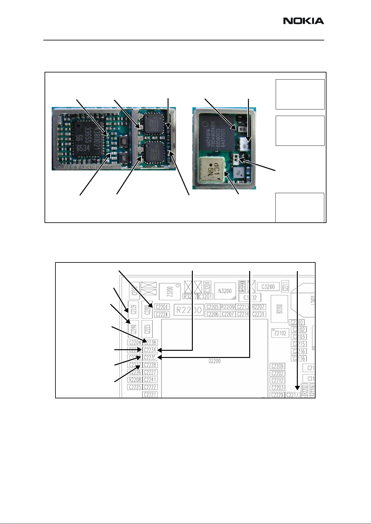
Bluetooth DC and RF Probe Points
Figure 61 shows the Bluetooth DC and RF probe points.
VDD_VCO and
VDD_RADIO
RF IN/OUT
Bluetooth
1.8V
VDD_ANA
1.8V
VIO
1.8V
Filter
VDD_VCO and
VDD_RADIO
1.8V
Figure 61: Bluetooth DC and RF Probe points
Vbatt
Bluetooth
ASIC
VIO
1.8V
Page 64 Company Confidential Issue 1 - September 2006
 Loading...