

Page 1

PAMS Technical Documentation
NHX-7 Transceiver
Chapter 2
Baseband Module JP3
Original 10/98
Page 2

NHX-7
PAMS
Baseband Module JP3
AMENDMENT RECORD SHEET
Amendment
Number
Date Inserted By Comments
10/98 Original
Technical Documentation
Page 2 – 2
Original 10/98
Page 3

PAMS
NHX-7
Technical Documentation
CONTENTS
System Module JP3: Introduction 2 – 6. . . . . . . . . . . . . . . . . . . . . . . .
Baseband Sub-module 2 – 6. . . . . . . . . . . . . . . . . . . . . . . . . . . . . . . . . .
Block Diagram of baseband 2 – 7. . . . . . . . . . . . . . . . . . . . . . . . . . . .
Technical summary 2 – 8. . . . . . . . . . . . . . . . . . . . . . . . . . . . . . . . . . .
Modes of Operation 2 – 8. . . . . . . . . . . . . . . . . . . . . . . . . . . . . . . . . . .
CTRLU Circuit 2 – 10. . . . . . . . . . . . . . . . . . . . . . . . . . . . . . . . . . . . . . .
Block Description 2 – 10. . . . . . . . . . . . . . . . . . . . . . . . . . . . . . . . . .
Extended standby mode for power saving 2 – 11. . . . . . . . . . .
Main Components 2 – 11. . . . . . . . . . . . . . . . . . . . . . . . . . . . . . . . . .
MCU 2 – 11. . . . . . . . . . . . . . . . . . . . . . . . . . . . . . . . . . . . . . . . . . .
EEPROM 2 – 14. . . . . . . . . . . . . . . . . . . . . . . . . . . . . . . . . . . . . . .
PWRU Circuit 2 – 14. . . . . . . . . . . . . . . . . . . . . . . . . . . . . . . . . . . . . . . .
Power Distribution 2 – 14. . . . . . . . . . . . . . . . . . . . . . . . . . . . . . .
Battery charging 2 – 16. . . . . . . . . . . . . . . . . . . . . . . . . . . . . . . . .
Startup charging 2 – 16. . . . . . . . . . . . . . . . . . . . . . . . . . . . . . . . .
Battery overvoltage protection 2 – 17. . . . . . . . . . . . . . . . . . . . .
Battery removal during charging 2 – 18. . . . . . . . . . . . . . . . . . .
Different PWM frequencies ( 1Hz and 32 Hz) 2 – 19. . . . . . . .
Charger Current measurement 2 – 20. . . . . . . . . . . . . . . . . . . .
Battery identification 2 – 21. . . . . . . . . . . . . . . . . . . . . . . . . . . . . .
Battery voltage measurement, VBATSW 2 – 22. . . . . . . . . . . .
Charger voltage measurement, VCHARG 2 – 23. . . . . . . . . . .
Charger current measurement 2 – 23. . . . . . . . . . . . . . . . . . . . .
Battery temperature 2 – 23. . . . . . . . . . . . . . . . . . . . . . . . . . . . . .
Vibra alerting device 2 – 24. . . . . . . . . . . . . . . . . . . . . . . . . . . . .
Supply voltage regulators and controlling 2 – 25. . . . . . . . . . .
Operation modes 2 – 27. . . . . . . . . . . . . . . . . . . . . . . . . . . . . . . .
Operation modes 2 – 28. . . . . . . . . . . . . . . . . . . . . . . . . . . . . . . . . . .
Power–Off Mode 2 – 28. . . . . . . . . . . . . . . . . . . . . . . . . . . . . . . . .
Entering Power–Off Mode 2 – 28. . . . . . . . . . . . . . . . . . . . . . . . .
Charging in Power–Off 2 – 29. . . . . . . . . . . . . . . . . . . . . . . . . . .
Reset Mode 2 – 29. . . . . . . . . . . . . . . . . . . . . . . . . . . . . . . . . . . . .
Power–On Mode 2 – 30. . . . . . . . . . . . . . . . . . . . . . . . . . . . . . . . .
Sleep Mode 2 – 30. . . . . . . . . . . . . . . . . . . . . . . . . . . . . . . . . . . . .
AUDIO 2 – 31. . . . . . . . . . . . . . . . . . . . . . . . . . . . . . . . . . . . . . . . . . . . . .
Audio Control 2 – 31. . . . . . . . . . . . . . . . . . . . . . . . . . . . . . . . . . . . . .
Internal microphone 2 – 31. . . . . . . . . . . . . . . . . . . . . . . . . . . . . . . .
Internal earphone 2 – 31. . . . . . . . . . . . . . . . . . . . . . . . . . . . . . . . . .
Buzzer 2 – 31. . . . . . . . . . . . . . . . . . . . . . . . . . . . . . . . . . . . . . . . . . . .
Headset detection 2 – 31. . . . . . . . . . . . . . . . . . . . . . . . . . . . . . . . . .
Headset Switch detection 2 – 31. . . . . . . . . . . . . . . . . . . . . . . . . . .
Baseband Module JP3
Page No
Original 10/98
Page 2 – 3
Page 4

NHX-7
PAMS
Baseband Module JP3
NASTA ASIC 2 – 32. . . . . . . . . . . . . . . . . . . . . . . . . . . . . . . . . . . . . .
Main features 2 – 32. . . . . . . . . . . . . . . . . . . . . . . . . . . . . . . . . . . . . .
Transmit (TX) audio signal path 2 – 34. . . . . . . . . . . . . . . . . . . .
RECEIVE (RX) AUDIO SIGNAL PATH 2 – 36. . . . . . . . . . . . . .
Transmitting data path 2 – 37. . . . . . . . . . . . . . . . . . . . . . . . . . . .
Receiving data path 2 – 37. . . . . . . . . . . . . . . . . . . . . . . . . . . . . .
IF 2 – 37. . . . . . . . . . . . . . . . . . . . . . . . . . . . . . . . . . . . . . . . . . . . . .
AFC 2 – 38. . . . . . . . . . . . . . . . . . . . . . . . . . . . . . . . . . . . . . . . . . . .
ST signalling tone generator 2 – 38. . . . . . . . . . . . . . . . . . . . . . .
Standby Modes for Power Saving 2 – 38. . . . . . . . . . . . . . . . . .
RF Section 2 – 39. . . . . . . . . . . . . . . . . . . . . . . . . . . . . . . . . . . . . . . . . .
Technical Summary 2 – 39. . . . . . . . . . . . . . . . . . . . . . . . . . . . . . . .
Basic Specification 2 – 39. . . . . . . . . . . . . . . . . . . . . . . . . . . . . . . . .
RF Module Characteristics 2 – 40. . . . . . . . . . . . . . . . . . . . . . . . . . . . .
Maximum ratings 2 – 40. . . . . . . . . . . . . . . . . . . . . . . . . . . . . . . . . . .
DC Characteristics 2 – 40. . . . . . . . . . . . . . . . . . . . . . . . . . . . . . . . .
Regulator 2 – 40. . . . . . . . . . . . . . . . . . . . . . . . . . . . . . . . . . . . . . .
Battery Save at Reception Mode 2 – 40. . . . . . . . . . . . . . . . . . .
Control Signals 2 – 40. . . . . . . . . . . . . . . . . . . . . . . . . . . . . . . . . .
Power Distribution Diagram 2 – 41. . . . . . . . . . . . . . . . . . . . . . .
Connections 2 – 42. . . . . . . . . . . . . . . . . . . . . . . . . . . . . . . . . . . . . . . . .
Connections to Baseband module 2 – 42. . . . . . . . . . . . . . . . . .
Antenna 2 – 45. . . . . . . . . . . . . . . . . . . . . . . . . . . . . . . . . . . . . . . . . .
Functional description of radio sub–module 2 – 46. . . . . . . . . . . . . .
Block diagram 2 – 46. . . . . . . . . . . . . . . . . . . . . . . . . . . . . . . . . . . . .
RF components 2 – 47. . . . . . . . . . . . . . . . . . . . . . . . . . . . . . . . . . . .
Receiver 2 – 47. . . . . . . . . . . . . . . . . . . . . . . . . . . . . . . . . . . . . . . . . .
RX Synthesizer 2 – 47. . . . . . . . . . . . . . . . . . . . . . . . . . . . . . . . . . . .
RX loop filter 2 – 48. . . . . . . . . . . . . . . . . . . . . . . . . . . . . . . . . . . .
TX Synthesizer 2 – 48. . . . . . . . . . . . . . . . . . . . . . . . . . . . . . . . . . . .
TX Loop Filter 2 – 48. . . . . . . . . . . . . . . . . . . . . . . . . . . . . . . . . . .
Transmitter 2 – 48. . . . . . . . . . . . . . . . . . . . . . . . . . . . . . . . . . . . . . . .
RF Characteristics 2 – 49. . . . . . . . . . . . . . . . . . . . . . . . . . . . . . . . . . . .
Duplexer 2 – 49. . . . . . . . . . . . . . . . . . . . . . . . . . . . . . . . . . . . . . . . . .
RX submodule 2 – 49. . . . . . . . . . . . . . . . . . . . . . . . . . . . . . . . . . . . .
Preamplifier 2 – 50. . . . . . . . . . . . . . . . . . . . . . . . . . . . . . . . . . . . .
SAW–filter 2 – 51. . . . . . . . . . . . . . . . . . . . . . . . . . . . . . . . . . . . . .
1st mixer 2 – 51. . . . . . . . . . . . . . . . . . . . . . . . . . . . . . . . . . . . . . .
1st IF–filter 2 – 52. . . . . . . . . . . . . . . . . . . . . . . . . . . . . . . . . . . . . .
IF–amplifier 2 – 52. . . . . . . . . . . . . . . . . . . . . . . . . . . . . . . . . . . . .
2nd if–filter 2 – 52. . . . . . . . . . . . . . . . . . . . . . . . . . . . . . . . . . . . . .
IF–circuit 2 – 53. . . . . . . . . . . . . . . . . . . . . . . . . . . . . . . . . . . . . . .
TX submodule 2 – 53. . . . . . . . . . . . . . . . . . . . . . . . . . . . . . . . . . . . .
Power amplifier 2 – 54. . . . . . . . . . . . . . . . . . . . . . . . . . . . . . . . . .
Power control circuit 2 – 55. . . . . . . . . . . . . . . . . . . . . . . . . . . . . .
Technical Documentation
Page 2 – 4
Original 10/98
Page 5

PAMS
NHX-7
Technical Documentation
Synthesizer submodule 2 – 55. . . . . . . . . . . . . . . . . . . . . . . . . . . . .
PLL circuit for RX local oscillator signal and TX injection 2 – 55
RX local oscillator signal 2 – 55. . . . . . . . . . . . . . . . . . . . . . . . . .
TX VCO 2 – 56. . . . . . . . . . . . . . . . . . . . . . . . . . . . . . . . . . . . . . . .
TX buffers 2 – 57. . . . . . . . . . . . . . . . . . . . . . . . . . . . . . . . . . . . . .
VCTCXO 2 – 57. . . . . . . . . . . . . . . . . . . . . . . . . . . . . . . . . . . . . . . . . .
Parts list of JP3 (EDMS Issue 4.3) Code: 0201185 2 – 58. . . . . . . . . .
Baseband Module JP3
Schematic Diagrams
Block Diagram (Version 07 Edit 128) for layout version 08 3/A3–1. . .
Circuit Diagram of PWRU + CONNECTOR (Version 08 Edit 224)
for layout version 08 3/A3–2. . . . . . . . . . . . . . . . . . . . . . . . . . . . . . . . . . . . .
Page No
Circuit Diagram of CTRLU Block (Version 08 Edit 21)
for layout version 08 3/A3–3. . . . . . . . . . . . . . . . . . . . . . . . . . . . . . . . . . . . .
Circuit Diagram of Audio (Version 08 Edit 308)
for layout version 08 3/A3–4. . . . . . . . . . . . . . . . . . . . . . . . . . . . . . . . . . . . .
Circuit Diagram of Transmitter (Version 07 Edit 125)
for layout version 08 3/A3–5. . . . . . . . . . . . . . . . . . . . . . . . . . . . . . . . . . . . .
Circuit Diagram of Receiver (Version 07 Edit 166)
for layout version 08 3/A3–6. . . . . . . . . . . . . . . . . . . . . . . . . . . . . . . . . . . .
Circuit Diagram of Synthesizer (Version 07 Edit 168)
for layout version 08 3/A3–7. . . . . . . . . . . . . . . . . . . . . . . . . . . . . . . . . . . .
Layout Diagram of US4U (Layout version 08) 3/A3–8. . . . . . . . . . . . . .
Original 10/98
Page 2 – 5
Page 6

NHX-7
PAMS
Baseband Module JP3
System Module JP3: Introduction
This document specifices the System module JP3 of the NHX–7 ETACS
cellular phone.
The JP3 System Module comprises the baseband and the RF functions of
the phone.
Baseband Sub-module
The Baseband submodule controls the internal operation of the phone. It
controls the user interface, i.e. LCD driver, keyboard and audio interface
functions. The module performs all signalling towards the system and carries out audio–frequency signal processing. In addition, it controls the operation of the transceiver and stores tuning data for the phone.
The baseband architecture is basically similar to the previous generation.
However, the system specified logical voltage level used is 2.82V and
new features include a improved charging circuit CHAPS and a new power supply circuit PSA.
Technical Documentation
The baseband architecture supports a power saving function called ”extended standby mode”. This sleep mode shuts off the Receiver and part
of the NASTA blocks. The phone is woken up at every FOCC:s first word
and it is ”sleeping” the rest of the time.
The nominal battery voltage in NHX–7 is 3.6V. The actual battery voltage
varies between 3.0 to 4.2V/5.3V depending on the used cell type (Li-Ion
or NiMH) and whether the phone is connected to a charger (limit on 5.3V
with NiMH battery in idle).
Battery charging is controlled by a PWM signal from the MCU. The PWM
duty cycle is determined by a charging software. The PWM signal is fed
to the CHAPS charging switch and through the charging pins to an external charger. There can be two types of chargers connected to the phone.
Standard chargers (two wires) provide coarse supply power, which is
switched by the CHAPS for suitable charging voltage and current.
Advanced chargers (three wires) are equipped with a control input,
through which the phone gives PWM charging control signal to the charger.
Page 2 – 6
Original 10/98
Page 7
PAMS
NHX-7
Technical Documentation
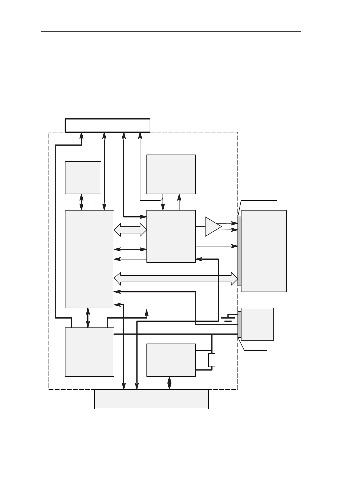
Block Diagram of baseband
Rf power
supply
EEPROM
4k byte
32 byte
OTP
Rf control Mod/Daf Ref
Clock
VCTCXO
System
14.85 MHz
Baseband Module JP3
Clock
UI
MCU
H8 3093
4kx8 RAM
192k ROM
8 ADC
I/O Ports
Serial ports
PWM
outputs
PSA
Power
Supply
Asic
Data
NASTA
Audio/
Audio
control
McuClk
Rows, Cols, Disp data, Lights, Buzz
Power supply VL,VA
Signalling
BSI, BTEMP
BaseBand
Asic
LcdClk
CHAPS
Charger
Asic
Vbat
Earp
Earn
Ichar
Current
Shunt
Connector
UI Board
Display/
Driver
Keypads
Earphone
Buzzer
Lights
Battery
Battery
Connector
Original 10/98
System Connector:
Mbus,Xmic,Xear ,Mic
Bottom connector
Charger Connector:
Vcharg, Charger cntl, Gnd
Figure 1.
Page 2 – 7
Page 8

NHX-7
PAMS
Baseband Module JP3
Technical summary
The baseband module consists of VCTCXO module and four ASIC circuits, PSA, CHAPS, NASTA 4.5, EEPROM, and some standard circuits,
DUAL BILATERAL SWITCH (TC7W66F), AUDIO POWER AMPLIFIER
(LM4862) and a Hitachi H8 series controller (H8/3093 MCU).
The MCU includes memories, 192 kbytes ROM and 4 kbytes RAM. It
controls all transceiver functions.
The EEPROM type is 4 kbytes with 32 bytes. The OTP memory is a seri-
2
C–bus type.
al I
The baseband is running from a 2.8 V power rail, which is supplied by a
power controlling asic. In the PSA asic there are two separate power supplies for BaseBand ( VA,VL ) and two externally controllable power supplies for RF (VRX, VTX).
The CHAPS is a charging control ASIC. It is essentially
power switch for controlling charging current, in a mobile phone. CHAPS
is designed for 3 cell Nickel or 1 cell Lithium battery packs.
Technical Documentation
an integrated
The NASTA circuit integrates the Audio and Modem operations. Because
the NASTA supports only one microphone, there are two bilateral
switches to connect the internal microphone or the headset microphone
to the NASTA MIC input. There is an audio power amplifier for EAR and
XEAR lines each. The internal earphone amplifier is a dual ended type
output which is in EAR line and there is transistor buffer in XEAR line.
The VCTCXO module is a voltage and temperature controlled oscillator
which operates as system clock for RF and BaseBand.
All functional blocks of the baseband are mounted on a single multi layer
printed circuit board. All components of the baseband are surface mountable. This board contains also the RF–parts. The B–cover side ( battery
side ) EMC shielding is implemented by using a metallic RF–shields on
the RF–blocks. On the other side the engine is shielded with a aluminium
frame, which makes a contact to a ground ring of the engine board and a
ground plane of the UI–board.
The connections from BaseBand to UI board are fed through a 28–way
2–row board to board spring connector.
Page 2 – 8
Original 10/98
Page 9

PAMS
NHX-7
Technical Documentation
Modes of Operation
Power off, Standby, Listening and Conversation modes.
– In Power off mode only the circuits needed for power up are supplied.
– In Standby mode the MCU and needed blocks of the NASTA are ac-
tive.
– In Listening mode the receiver and some blocks of the NASTA are ac-
tive.
– In Conversation mode all ICs are active.
Baseband Module JP3
Original 10/98
Page 2 – 9
Page 10

NHX-7
PAMS
Baseband Module JP3
CTRLU Circuit
The Control block CTRLU controls all functions of the phone.
Block Description
– CTRLU – PWRU
CTRLU controls the watchdog timer in PSA. It sends a negative pulse at
approximately 0,1 s to XPWROFF pin of the PSA to keep the power on. If
CTRLU fails to deliver this pulse, the PSA will remove power from the
system. When power off is requested CTRLU leaves PSA watchdog without reset. After the watchdog has elapsed PSA cuts off the supply voltages from the phone. CTRLU controls also the charger on/off switching in
the PWRU block. Battery charging is controlled by CSW line, which is
PWM–controlled output port.
Technical Documentation
– CTRLU – AUDIO
Interface between microcontroller and the NASTA circuit is bidirectional
8–bit data bus with 4 address lines. Address, data and control lines are
used in microcontroller as I/O–port pins. Data lines direction must be controlled with microcontroller data direction register. Interface includes address outputs NA0–3, data inputs (read) / outputs (write) ND0–7, chip select control output XNCS , read control output XNRD, write control output
XNWR and interrupt input XINT. To minimize power consumption, control
signals XRD and XCS should be in ’0’ state and address output NA0–3
and NWR in ’1’ state and data lines ND0–7 should be inputs .Buzzer is
controlled by BUZZ_DRV PWM signal. Headset adapter is detected by
HSCONN input.
– CTRLU – UIF and DISPLAY
Keyboard is connected directly to the controller. COL 0:3 are output lines
and ROW 0:3 are input lines. Watchdog is updated same time with keyboard scanning (XPWROFF). Keyboard scanning is done by driving one
COL to 0 V at time and ROWs are used to read which key is pressed.
Keyboards lights are controlled by KEYBLIGHT signal and LCD lights by
LCDBLIGHT signal.
LCD controller interface to microcontroller is a bidirectional data line
LCDDA, data serial clock line SCLK output, chip select control LCDENX
output, command or display data control LCDDC output and reset control
LCDRES output.
– CTRLU – RECEIVER
Received signal strength is measured over the RSSI line and intermediate frequency is measured over the IF line.
RX synthesizer and receiver are powered on/off by PSBS_EN line.
Page 2 – 10
Original 10/98
Page 11

PAMS
NHX-7
Technical Documentation
– CTRLU – SYNTHESIZER
Frequency is controlled by the AFC signal. The synthesizer is controlled
via the synchronous serial bus SDAT/SCLK. The data is latched to the
synthesizer by the positive edge of the SLE line. The TX synthesizers
power on/off is controlled by VTX_ENA signal.
– CTRLU – TRANSMITTER
The transmitter on/off state is detected over the TXI line. The TXE line activates the power module. The power is controlled via the TXC line which
is a PWM–controlled output port (frequency about 9.4 kHz).
Extended standby mode for power saving
The extended standby mode is automatically activated when the phone is
working in the control channel (FOCC). The NASTA runs this function,
switching on/off the receiver’s power supply.
PSPS_EN signal:
– The signal connects the RX regulator on via the PSA when it is in ”1”
state, in ”0” state the RX regulator is off.
Baseband Module JP3
HPD_EN signal:
– The signal controls the RX synthesizers hardware power down function.
When it is in ”1” state the RX synthesizer is powered up, in ”0” state the
RX synthesizer is powered down.
Main Components
MCU
The H8/3093 is a CMOS microcontroller. All the memory needed 192kB
ROM, 4kB RAM) except the EEPROM, is located in the controller. The
MCU operating clock (2.4 MHz) is generated on the NASTA and the
VCTCXO. The H8/3093 is operating in single–chip normal mode (mode
3) 192kbyte address space, so all input/output pins are used as I/O–ports.
Pin Number Port Signal Description
1 PB0 SDAT
2 PB1 RSSI_READY RSSI readings synchronization
3 PB2 VIBRA_CONTROL Vibra alerting device on/off
4 PB3 RXD
Synthesizer data line
M2BUS net free timer input
5 PB4 EAREN
6 PB5 XPWROFF
7 PB6 PWRON
8 PB7 SLE
9 P90 TXD
Original 10/98
Earphone amplifier enable
Power off control
Power button state
Synthesizer latch enable
Serial interface (M2BUS)
Page 2 – 11
Page 12

NHX-7
PAMS
Baseband Module JP3
10 P92 RXD
11 P94 ECLK
12 VSS GND
13 – 20 P30 – P37 ND0 – ND7
21 VCC VL
22 P10 NA0
23 P11 NA1
24 P12 NA2
25 P13 NA3
26 P14 XNCS
27 P15 XNWR
28 P16 XNRD
Technical Documentation
DescriptionSignalPortPin Number
Serial interface (M2BUS)
Serial data clock for EEPROM
Parallel data bus for NASTA
Address line for NASTA
Address line for NASTA
Address line for NASTA
Address line for NASTA
NASTA chip select
Write control to NASTA
Read control to NASTA
29 P17 LIGHTS
30 VSS GND
31 – 34 P20 – P23 COL0–COL3
35 – 38 P24 – P27 ROW0 – ROW3
39 P50 SCLK
40 P51 LCDENX
41 P52 LCDDC
42 P53 LCDSDA
43 P60 VTX_ENA
44 – 45 MD0 – MD1
46 NC NC
47 STBY VL
48 RES XRES
49 NMI NC
50 VSS GND
Keypad backlight control
Keypad outputs
Keypad inputs (Input pullup used)
Serial data clock for lcd driver
Chip select signal for lcd driver
Display or Command data
Data line for lcd driver
TX synthesizer enable. Active
high
Mode selection
Reset from PSA
51 EXTAL CLKMCU
52 XTAL NC
53 VCC VL
54 P63 TXE
55 P64 LIM
Page 2 – 12
External system clock from
NASTA
Transmitter on/off
Battery cut off limit selection
Original 10/98
Page 13

PAMS
NHX-7
Technical Documentation
56 P65 XEAR_EN
57 RESO NC
58 AVSS GND
59 P70 VBATSW
60 P71 VCHARG
61 P72 ICHAR
62 P73 BTEMP
63 P74 RSSI
64 P75 TXI
65 P76 HSCON
66 P77 BSI
67 VREF VA
Baseband Module JP3
DescriptionSignalPortPin Number
Headset earpiece amplifier control
Battery voltage
Charger voltage
Charging current measurement
Battery temperature
Received signal strength
Transmitter state monitor
Headset detecting voltage
Battery size indicator
68 AVCC VA
69 P80 XINT
70 P81 LCDRES
71 P82 LCDBLIGHT
72 P83 HEADSW
73 PA0 MIC_EN
74 PA1 LCDCLK
75 PA2 BUZZ_DRV
76 PA3 SCLK
77 PA4 CSW
78 PA5 EDATA
79 PA6 TXC
80 PA7 XMIC_EN
Interrupt request from NASTA
LCD reset signal
LCD backlight control
Headset switch indicator
Internal microphone control
LCD clock from NASTA
PWM output for buzzer
Serial clock for synthesizer
Charging control PWM
Eeprom data line
Transmitter power control
Headset microphone control
Original 10/98
Page 2 – 13
Page 14
NHX-7
PAMS
Baseband Module JP3
EEPROM
There is one 4kbyte EEPROM with 32byte OTP memory in the phone.
The EEPROM is a nonvolatile memory in which the tuning data for the
phone is stored. In addition, it contains the short code memory locations
to retain user selectable phone numbers. The OTP memory is ROM area
for identification and security purposes.
Table 1. EEPROM signals:
Pin No Signal Description
5 SDA
6 SCL
I2C bus data
I2C bus clock
PWRU Circuit
Technical Documentation
Power Distribution
The main components of the Power Unit are the PSA ( Power Supply
Asic) and the CHAPS ( Charger Power Switch ).
In normal operation the baseband is powered from the phone‘s battery.
The battery consists of three Nickel Metal Hydride cells. There is also a
possibility to use batteries consisting of one Lithium–Ion cell. An external
charger is used for recharging the battery and supplying power to the
phone. The charger can be either a standard charger that can deliver
around 400 mA or a so called performance charger, which can deliver
supply current up to 850 mA.
The baseband contains components that control the power distribution to
the whole phone excluding those parts that use continuous battery supply. The battery feeds power directly to three parts of the system: PSA,
RF–power amplifier, and UI (buzzer and display and keyboard lights).
The power management circuit CHAPS provides protection against overvoltages, charger failures and pirate chargers etc. that could otherwise
cause damage to the phone.
Signal
name
VBATT Battery
From
To
RF/UIF
Table 2. DC Characteristics of PWRU signals
Parameter Mini-
mum
Voltage 3.0 3.6 5.0/5.3 V
Current 3500 mA
Typi-
cal
Maxi-
mum
Unit Function
Supply voltage for RF
and UIF
XRES PSA
MCU,NAST A,UIF
Page 2 – 14
Logic high ”1” 0.7*VL VL V PSA is Power On
Mode
Logic low ”0” 0 0.3*VL V PSA is Power Off or
Reset Mode
Original 10/98
Page 15

PAMS
CHAPS
S
d
NHX-7
Technical Documentation
Table 2. DC Characteristics of PWRU signals (continued)
Signal
PSA
MCU
PSA
MCU
To
Logic high ”1” VL–0.5 VL V Cutoff limit 5.0 V
Logic low ”0” 0 0.4 V Cutoff limit 4.6 V
Logic high ”1” 0.7*
Logic low ”0” 0 1.2 V Power On switch
Logic high ”1” VL–0.5 VL V Watchdog counter not
Logic low ”0” 0 0.4 V Watchdog counter re-
Logic high ”1” 0.7*VL VL V PSA is in Power On
Logic low ”0” 0 0.3*VL V PSA is in Power Off or
name
LIM MCU
XPWRON UIF
XPWR
OFF
PWRON PSA
Baseband Module JP3
ParameterFrom
Minimum
VBAT
Typi-
cal
mum
VBAT V Power On switch
open
closed
reset
set ”1” –> ”0”
Mode
Reset mode
FunctionUnitMaxi-
PSBS_EN
(Phone
upporte
Battery
Save)
HPD_EN NAST A
VTX_ENA MCU
VBATSW PSA
VCHARG PSA
ICHAR AMPLIFI-
NASTA
PSA
PLL circuit
PSA
MCU
MCU
ER
MCU
Logic high ”1” 2.0 2.90 V VRX Enabled
Logic low ”0” 0 0.5 V VRX Disabled
Logic high ”1” 2.0 2.90 V Harware power down
disabled on PLL circuit
Logic low ”0” 0 0.4 V Hardware power down
enabled on PLL circuit
Logic high ”1” VL–0.5 VL V TX VCO and synthe-
sizer powered on
Logic low ”0” 0 0.4 V TX VCO and synthe-
sizer powered off
Voltage 0 2.45 V
VBATSW/VBAT di-
vision ratio
Voltage 0 2.8 V
VCHRSW switch
resistance
Voltage 0 2.90 V Charger Current Mea-
0.436 0.45 0.464
0 0.25 1.0 Kohm
Switched internally di-
vited VBA T voltage
Switched Charger volt-
age
surement over the
shunt resistor.
TXD MCU
PSA
Original 10/98
Logic high ”1” VL–0.5 VL V M2BUS data output,
PSA M2BUS output is
in high–Z state.
Logic low ”0” 0 0.4 V M2BUS data output,
PSA M2BUS output is
LOW
Page 2 – 15
Page 16
NHX-7
MCU
PSA
ACP–9
l
PAMS
Baseband Module JP3
Table 2. DC Characteristics of PWRU signals (continued)
Signal
name
To
RXD PSA
CSW MCU
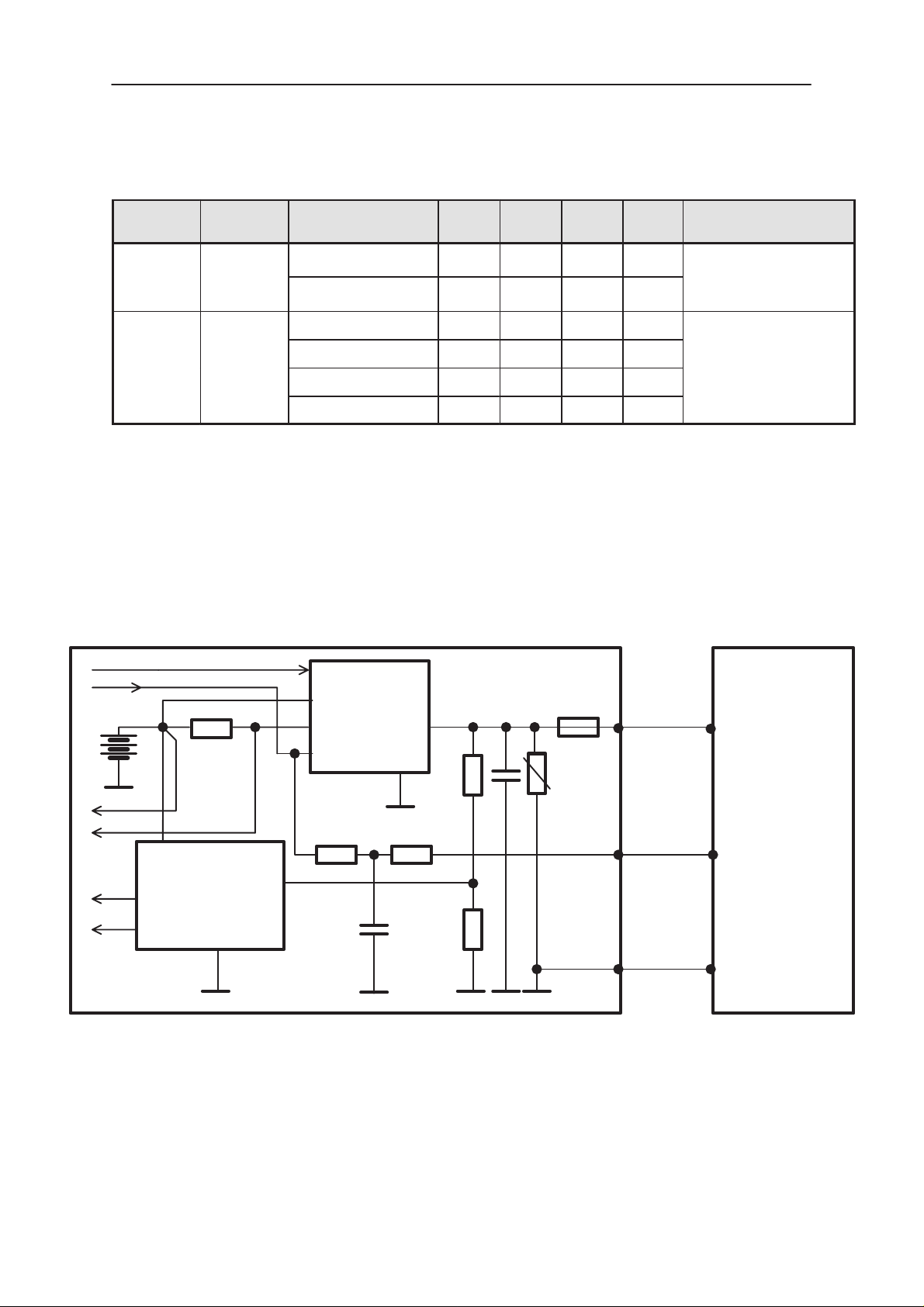
Battery charging
Acceptable chargers are detected by the software. The absolute maximum input voltage is 30V due to the transient suppressor that is protecting the charger input. At the phone end there is no difference between a
plug–in charger or a desktop charger. The DC–jack pins and bottom connector charging pads are connected together inside the phone. The
charging block diagram is below.
Technical Documentation
ParameterFrom
Minimum
Logic high ”1” 2.0 2.90 V
Logic low ”0” 0 0.5 V
Logic high ”1” 2.0 2.90 V
Logic low ”0” 0 0.5 V
PWM frequency 1 32 Hz
PWM duty cycle 0 100 %
Typi-
cal
mum
FunctionUnitMaxi-
M2BUS data input
Charger switch and
control signa
LIM
CSW
MCU
MCU
0R22
VBAT
VBATSW
VCHARGSW
PSA
GND
VCHAR
LIM
VOUT
RSENSE
PWM
10k
27p
CHAPS
VCH
GND
TRANSCEIVER
1u
50.3k
10k
10k
Figure 2. Charging block diagram
30V
2A
VIN
CHRG_CTRL
L_GND
CHARGER
NOT IN
ACP–7
Startup charging
When a charger is connected, the CHAPS is supplying a startup current
minimum of 130mA to the phone. The startup current provides initial
Page 2 – 16
Original 10/98
Page 17
PAMS
NHX-7
Technical Documentation
Baseband Module JP3
charging to a phone with an empty battery. The startup circuit charges
the battery until the battery voltage level reaches 3.0V (+/– 0.1V) and the
PSA releases the PURX reset signal and program execution starts.
Charging mode is changed from startup charging to PWM charging that is
controlled by the MCU software. If the battery voltage reaches 3.55V
(3.75V maximum) before the program has taken control over the charging, the startup current is switched off. The startup current is switched on
again when the battery voltage has decreased to 100mV (nominal).
Table 3. Startup characteristics
Parameter Symbol Min Typ Max Unit
VOUT Start– up mode cutoff limit Vstart 3.45 3.55 3.75 V
VOUT Start– up mode hysteresis
NOTE: Cout = 4.7 uF
Start–up regulator output current
VOUT = 0V ... Vstart
Vstarthys 80 100 200 mV
Istart 130 165 200 mA
Battery overvoltage protection
Output overvoltage protection is used to protect phone from damage.
This function is also used to define the protection cutoff voltage for different battery types (Li or Ni). The power switch is immediately turned OFF if
the voltage in VOUT rises above the selected limit VLIM1 or VLIM2.
Table 4. VLIM characteristics
Parameter Symbol LIM input Min Typ Max Unit
Output voltage cutoff limit (dur-
ing transmission or Li–battery)
Output voltage cutoff limit (no
transmission or Ni–battery)
VLIM1 LOW 4.4 4.6 4.8 V
VLIM2 HIGH 4.8 5.0 5.2 V
The voltage limit (VLIM1 or VLIM2) is selected by logic LOW or logic
HIGH on the CHAPS (N101) LIM– input pin. Default value is lower limit
VLIM1.
When the switch in output overvoltage situation has once turned OFF, it
stays OFF until the the battery voltage falls below VLIM1 (or VLIM2) and
PWM = LOW is detected. The switch can be turned on again by setting
PWM = HIGH.
Original 10/98
Page 2 – 17
Page 18
NHX-7
PAMS
Baseband Module JP3
VCH
VCH<VOUT
VOUT
VLIM1 or VLIM2
SWITCH
ON OFF
Technical Documentation
t
t
ON
PWM (32Hz)
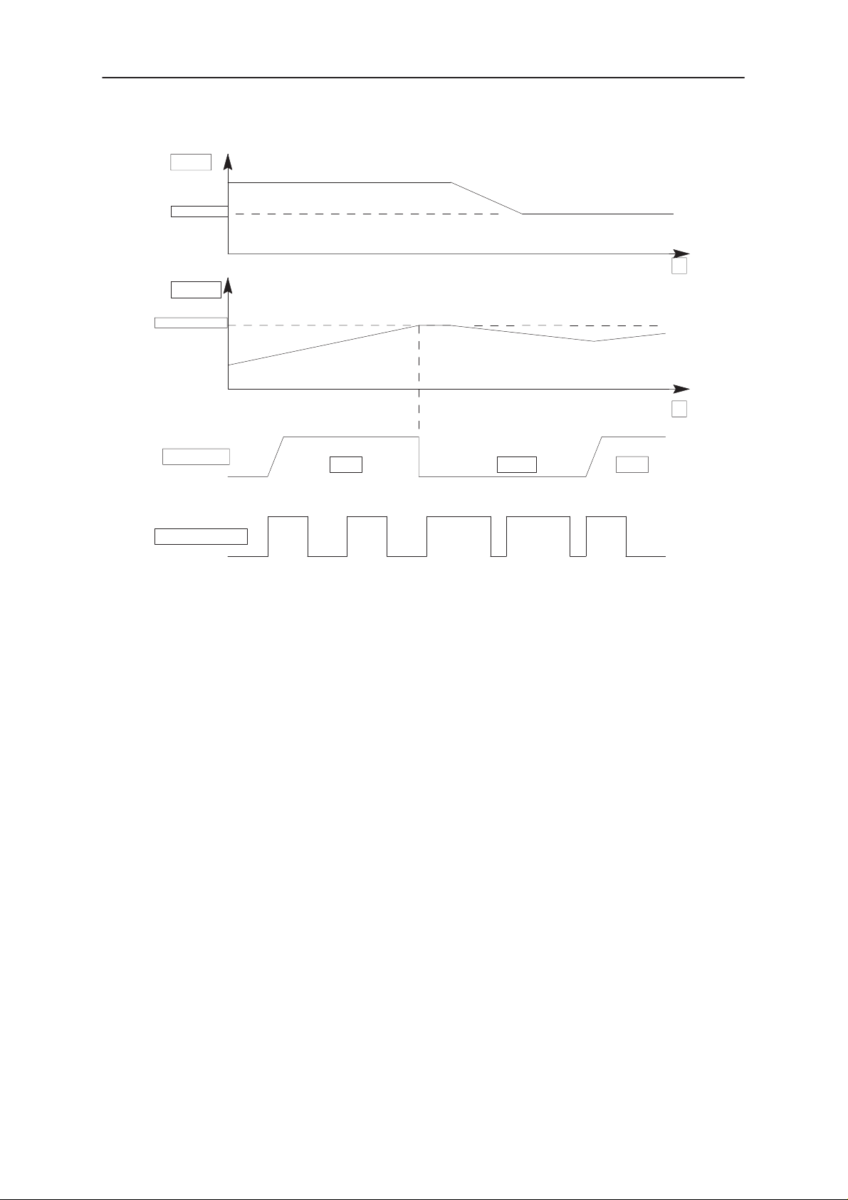
Figure above: Battery overvoltage protection
Battery removal during charging
Output overvoltage protection is also needed in case the main battery is
removed when a charger connected or a charger is connected before the
battery is connected to the phone.
With a charger connected, if VOUT exceeds VLIM1 (or VLIM2), the
CHAPS turns switch OFF until the charger input has decreased below
Vpor (nominal 3.0V, maximum 3.4V). The MCU software stops the charging (turn off PWM) when it detects that the battery has been removed.
The CHAPS remains in protection state as long as the PWM stays HIGH
after the output overvoltage situation has occurred.
Page 2 – 18
Original 10/98
Page 19
PAMS
NHX-7
Technical Documentation
VCH
(Standard
Charger)
VOUT
PWM
Vpor
VLIM
4V
Vstart
”1”
”0”
Droop depends on load
& C in phone
Baseband Module JP3
Istart off due to VCH<Vpor
Vstarthys
t
t
SWITCH
1.1Battery removed, (standard) charger connected, VOUT rises (follows charger voltage)
2. VOUT exceeds limit VLIM(X), switch is turned immediately OFF
3.3VOUT falls (because no battery) , also VCH<Vpor (standard chargers full–rectified
4. Software sets PWM = LOW –> CHAPS does not enter PWM mode
5. PWM low –> Startup mode, startup current flows until Vstart limit reached
6. VOUT exceeds limit Vstart, Istart is turned off
7. VCH falls below Vpor
ON
OFF
2
output). When VCH > Vpor and VOUT < VLIM(X) –> switch turned on again (also PWM
is still HIGH) and VOUT again exceeds VLIM(X).
5
4
Figure above: Battery removal during charging
Different PWM frequencies ( 2Hz and 32 Hz)
When a travel charger (2– wire charger) is used, the power switch is
turned ON and OFF by the PWM input when the PWM rate is 2Hz. When
the PWM is HIGH, the switch is ON and the output current Iout = charger
current – CHAPS supply current. When PWM is LOW, the switch is OFF
and the output current Iout = 0. To prevent the switching transients inducing noise in audio circuitry of the phone soft switching is used.
6
7
t
The performance travel charger (3– wire charger) is controlled with PWM
at a frequency of 32Hz. When the PWM rate is 32Hz CHAPS keeps the
power switch continuously in the ON state.
Original 10/98
Page 2 – 19
Page 20
NHX-7
PAMS
Baseband Module JP3
SWITCH
PWM (2Hz)
SWITCH
Technical Documentation
ON ONON OFF OFF
ON
PWM (32Hz)
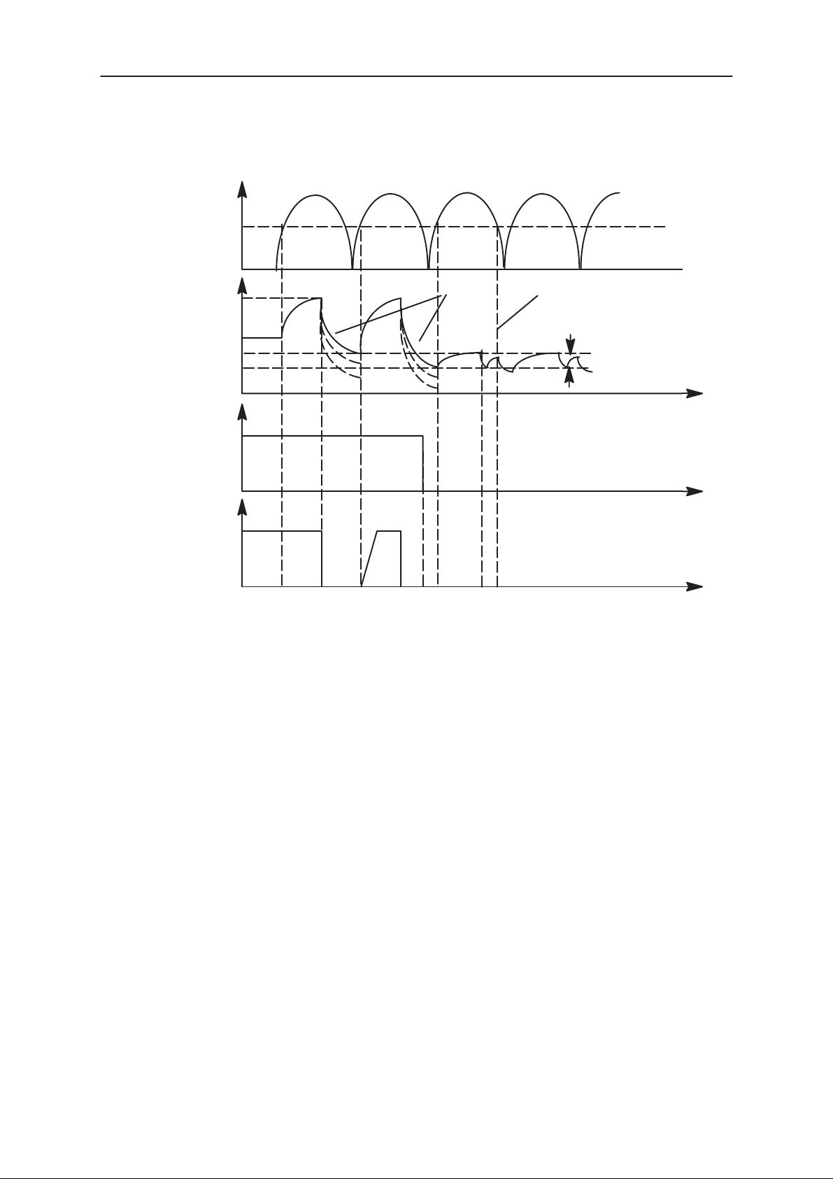
Figure 3. Switch control with 2Hz and 32 Hz frequencies (in this case 50% duty cycle)
Charger Current measurement
The charging current measurement is based on the reading of differential
voltages over the shunt resistor at the CHAPS output lines. The voltage is
measured and amplified by a differential amplifier and it is carried to the
MCU A/D converter. Measurement area is up to 1400 mA and 1 A/D bit
equals 1.85 mA. The charging current calibration is done with 0 mA and
500 mA in production test line. When charger is connected the current
measurement connection is activated. The A/D–conversion result and
charging current can be calculated from equations :
A/D readout = 1024 * V
Charging current:
I=(V
ICHAR
– V
(0mA)) * (500mA/(V
ICHAR
ICHAR
/ VREF
(500mA) – V
ICHAR
ICHAR
(0mA))
where VREF=2.82 V
Page 2 – 20
V
ICHAR
= voltage in ICHAR line
Original 10/98
Page 21
PAMS
ICHAR
NHX-7
Technical Documentation
Name Min Typ Max Unit Notes
V
ICHAR
From Charger input line
0.46 0.69 0.92 V
163 250 334 A/D
1.22 1.44 1.65 V
443 522 598 A/D
1.98 2.19 2.39 V
718 795 867 A/D
Baseband Module JP3
Table 5. Charger current measurement
Charging current is 0 mA. ( Calibration point )
Charging current is 500 mA. ( Calibration point )
Charging current is 1000 mA.
680k
100k
0R22
CHAPS
Ichar
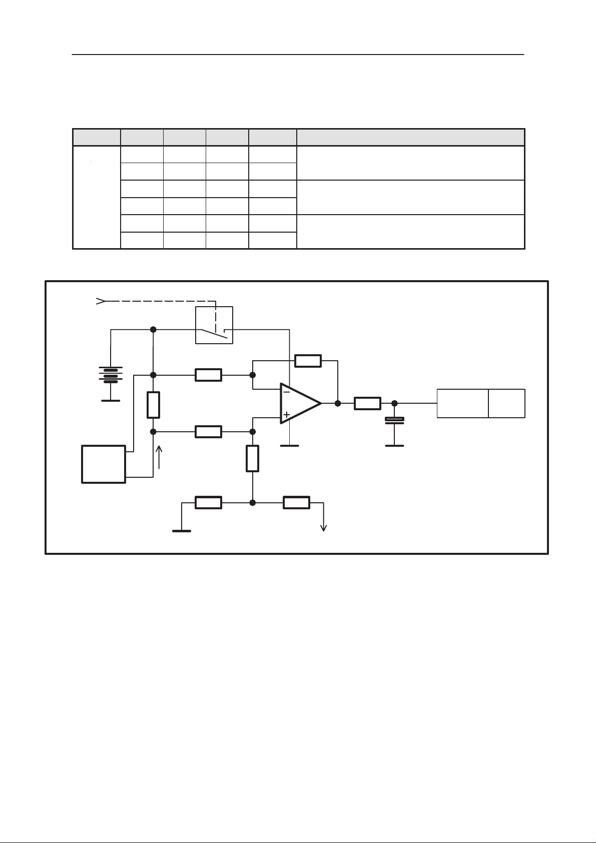
Battery identification
Different battery types are identified by a pull-down resistor inside the battery pack. The BSI line inside transceiver has a 22k pull-up to VA. The
MCU can identify a battery by reading the BSI line DC–voltage level with
a MCU (D201) A/D–converter.
22k
100k
680k
3k9
12k
+VA
Figure 4. Charger current measurement
1u
Ichar
A/D
conv.
MCU
Original 10/98
Page 2 – 21
Page 22

NHX-7
PAMS
Baseband Module JP3
Table 6. Battery Identification
Name Min Typ Max Unit Notes
BSI
0 2.8 V Battery size indication
22k pullup resistor to VA in phone
14.2 15 15.8 kohm Indication of a BMS–2V vibra battery (900mAh
9.5 10 10.5 kohm Indication of a BMS–2S battery (900mAh NiMH)
37 39 41 kohm Indication of a BLS–2 battery (900mAh LiIon)
48.5 51 53.5 kohm Indication of a BLS–4 battery (1600mAh LiIon)
–5 5 % Indication resistor and pullup resistor tolerance
Technical Documentation
NiMH)
BVOLT
BATTERY
BTEMP
2.8V
TRANSCEIVER
BSI
R
s
BGND
Battery voltage measurement, VBATSW
Battery voltage can be measured up to 6.27 V from the VBATSW line.
The absolute accuracy is low because of the voltage reference and
A/D–converter +/– 8 LSB accuracy . This battery voltage measurement
offset error must be calibrated with input voltage 4.1 V. The A/D conversion result can be calculated from equation:
A/D readout = 1024 * (VBAT* ( 0.45)) / VREF VREF=2.82 V
For example:
4.1 V results 670 = 29Dh
3.6 V results 588 = 24Ch
3.0 V results 490 = 1EAh
22k
10k
10n
BSI
A/D
Conv.
MCU
Charger voltage measurement, VCHARG
Charger voltage can be measured up to 17.00 V from VCHARG line. The
absolute accuracy is low because of the voltage reference and A/D–con-
Page 2 – 22
Original 10/98
Page 23

PAMS
NHX-7
Technical Documentation
Baseband Module JP3
verter +/– 8 LSB accuracy. The A/D–conversion result can be calculated
from equation :
A/D readout = 1024 * (VCHARG*(10/60.3)) / VREF VREF=2.82 V
For example:
8.4 V results 506 = 1F9h
Battery temperature
The battery temperature is measured with a NTC inside the battery pack.
The BTEMP line inside transceiver has a 100k pullup to VA. The MCU
can calculate the battery temperature by reading the BTEMP line DC–
voltage level with a MCU (D201) A/D–converter.
Table 7. Battery temperature
Pin Name Min Typ Max Unit Notes
3 BTEMP
0 2.90 V Battery temperature indication
100k pullup resistor to VA in phone
Battery package has NTC pull down resis-
tor:
47k +/–5%@+25C , B=4050+/–3%
–1 1 % 100k pullup resistor tolerance
BATTERY
R
T
NTC
BVOLT
BSI
BTEMP
BGND
TRANSCEIVER
VA
100k
10k
1k
BTEMP
MCU
CSW
10k
VibraPWM
ON/OFF
Battery temperature monitoring schematic diagram above
Based on 47k ± 5 % NTC with B = 4090 ±1.5 %. Without any alignment,
with that and 1 % pull–up resistor, ± 2.5 C accuracy is achieved between
– 20 and +60 C (± 3.5 C @ –40 ... +85 C).
Original 10/98
Page 2 – 23
Page 24

NHX-7
PAMS
Baseband Module JP3
Table 8. Battery temperature vs. AD readings and NTC resistance
T [C] AD R [k] T [C] AD R [k] T [C] AD R [k]
–40 963 1589 5 560 120.9 50 145 16.53
–35 942 1151 10 497 94.53 55 122 13.63
–30 915 842.8 15 436 74.40 60 103 11.30
–25 882 622.6 20 379 58.95 65 88 9.404
–20 842 464.1 25 327 47.00 70 74 7.865
–15 795 349.0 30 280 37.71 75 63 6.607
–10 743 264.6 35 238 30.43 80 54 5.573
–5 685 202.3 40 202 24.70 85 46 4.721
0 623 155.8 45 171 20.15 90 39 4.015
Technical Documentation
Vibra alerting device
A vibra alerting device is used for giving silent signal to the user of an incoming call. The device is not placed in the phone but it will be added to a
special battery pack. The vibra is controlled with a PWM signal by the
MCU via the BTEMP battery terminal.
Table 9. VIbra battery connection
Name Min Typ Max Unit Notes
BTEMP 9 11 14 kHz PWM control to VIBRA BATTERY
BSI
0 2.90 V Battery size indication
Phone has 100kohm pull up resistor.
14.2 15 15.8 kohm Battery size indication resistor (vibra battery)
A 15kohm BSI resistor is needed to detect the vibra battery. It is only used
to enable vibra selection in user menu. When alerting, VibraPWM signal
is delivered to battery.
Page 2 – 24
Original 10/98
Page 25

PAMS
NHX-7
Technical Documentation
Vibra
22k
10n
100n
BATTERY
R
T
47k
NTC
VBAT
BSI
BTEMP
GND
VA
100k
R3
1k
Baseband Module JP3
TRANSCEIVER
10k
BTEMP
MCU
CSW
10k
VIBRAPWM
ON/OFF
Figure 5. Vibra battery
Supply voltage regulators and controlling
The heart of the power distribution is the PSA asic. It includes all the voltage regulators and feeds power to the whole system. The baseband digital and analog parts are powered from the VL and VA regulators which
provide the 2.82 V baseband supply. The baseband regulators are active
when the phone is powered on.
The PSA includes also two 2.82 V regulators (VRX and VTX) providing
power to the RF section. These regulators can be controlled by the direct
control signals from the MCU. The VRX regulator can also be controlled
by the signal from the NASTA.
– VTX_ENA ( from MCU ) controls VTX regulator
– PSBS_ENA ( from NASTA ) controls VRX regulator
In addition PSA includes also functions listed bellow:
– Buffer for the M2BUS.
The buffer translates the logical input signal to open–drain output.
Table 10. M2BUS buffer truth table
Original 10/98
Input Output
LOW LOW
HIGH Z
Page 2 – 25
Page 26

NHX-7
PAMS
Baseband Module JP3
– Power on/off and reset logic. The Power off logic can be used as a
watchdog.
– Supply voltage monitor and automatic reset/power–off.
VBATSW is internally divided and buffered battery voltage output. The
A/D –converter input monitoring the battery voltage can be connected
here. The circuit monitors the voltage at the VBAT input and forces
the circuit to Reset if the voltage level is below allowed limit voltage,
VBATcoff–. A hysteresis is included to prevent oscillation between different states.
– Battery charger detection.
Externally divided charger voltage VCHAR goes through PSA internal
switch to VCHARSW output. The A/D –converter input monitoring the
charger voltage can be connected here.
– Automatic on–chip current limiting
– On–chip thermal shutdown, which protects PSA from overheating.
Thermal shutdown includes hysteresis in order to prevent oscillation
during the thermal protection.
Technical Documentation
Table 11. Regulators VA and VL characteristic
Parameter
Test Conditions
Output Voltage VL, V A 2.73 2.82 2.90 V
Output current of the regulator
(all regulators enabled)
Quiescent current
VL: Iload = 0mA
Iload = 40mA
VA: Iload = 0mA
Iload = 100mA
Quiescent current
Tamb = +25C, VBAT=3.6V
VL: Iload = 0mA
Iload = 40mA
VA: Iload = 0mA
Iload = 100mA
Quiescent current in Power–Off
VL
VA
Line regulation: VL, VA
IoutVL = 40mA,
IoutVL = 100mA,
3.25VVBAT5.2V
Symbol Limits
Min Typ Max
Iout
Iout
Iq
Iq
Iqoff
VL
line
VL
VA
, VA
line
040
0 100
200
220
200
220
110
130
110
130
6
15
20 mV
Unit
mA
mA
mA
mA
mA
mA
mA
mA
mA
mA
mA
mA
Load regulation: VL, VA
0mAIloadVL40mA,
0mAIloadVA100mA,
3.25VVBAT5.2V
Page 2 – 26
VL
load
, VA
load
30 mV
Original 10/98
Page 27

PAMS
NHX-7
Technical Documentation
Table 11. Regulators VA and VL characteristic (continued)
Test Conditions
Line transient:
AC=0.5V square wave
Slew rate = 50 mV/ms
f = 500Hz ... 2kHz
3.5VVBAT5.2V
Load transient: VL, VA
IloadVL 100mA to 40mA,
IloadVA 100mA to 100mA in
10ms
3.25VVBAT5.2V
Current limit (VL,VA = 0V)
VL
VA
Power Supply Ripple Rejection
3.2VVBAT5.2V
Baseband Module JP3
SymbolParameter
Min Typ Max
VL
r, VA
linet
V
Trec
Note 1
I
lim
PSRR 40 dB
linetr
40 dB
40
20
60 180
150 450
UnitLimits
mV
ms
mA
mA
0mAIloadVL40mA,
0mAIloadVA100mA
f = 10Hz ... 10kHz
Settling time
Cload=1mF20%
load current 0mA
ts
Note 2
160 ms
Note 1: Voltage deviation (V) is the output voltage overshoot in tran-
sient response. Recovery time (Trec) is the time from the beginning of the
transient response to the time point when the regulator output voltage first
crosses the final stable value after overshoot.
Note 2: Settling time is defined from the time point of mode change Power–Off to Reset to the time when regulator output voltage is within 5% of
the final value.
Table 12. Regulators VRX and VTX characteristic
Parameter
Test Conditions
Output Voltage VRX, VTX 2.73 2.82 2.90 V
Symbol Limits
Min Typ Max
Unit
Output currents of the regulators
(all regulators enabled)
Quiescent current
VRX: Iload = 0A
Iload = 50mA
VTX: Iload = 0A
Iload = 60mA
Original 10/98
Iout
Iout
Iq
VRX
VTX
0.05 50
0.02 60
320
360
320
360
mA
mA
mA
mA
mA
mA
Page 2 – 27
Page 28

NHX-7
PAMS
Baseband Module JP3
Table 12. Regulators VRX and VTX characteristic (continued)
Test Conditions
Quiescent current
Tamb = +25C, VBAT=3.6V
VRX: Iload = 0A
Iload = 50mA
VTX: Iload = 0A
Iload = 60mA
Quiescent current in Power–Off
VRX
VTX
Line regulation: VRX, VTX
IoutVRX = 50mA,
IoutVTX = 60mA,
3.25VVBAT5.2V
Load regulation: VRX, VTX
50mAIload
20mAIload
3.25VVBAT5.2V
VRX
VTX
50mA,
60mA,
SymbolParameter
Iq
Iqoff
VRX
VRX
line,
load,
VTX
VTX
line
load
Technical Documentation
UnitLimits
Min Typ Max
180
195
180
195
14
17
20 mV
30 mV
mA
mA
mA
mA
mA
mA
Line transient: VRX, VTX
AC=0.5Vpp square wave
Slew rate = 50 mV/ms
f = 500Hz .... 2kHz
3.5VVBAT5.2V
Load transient: VRX, VTX
Iload
50mA to 50mA,
VRX
IloadVTX 20mA to 60mA in 10ms
3.25VVBAT5.2V
Current limit (VRX,VTX = 0V)
VRX
VTX
Power supply ripple rejection
3.25VVBAT5.2V
50mAIload
20mAIload
VRX
VTX
50mA,
60mA,
f = 10Hz.....10kHz
f = 10Hz.....50kHz
f = 10Hz.....100kHz
Settling time,
Cload=1mF20%
load current 0mA
VRX
linetr,
V
Trec
Note 1
I
lim
PSRR
ts
Note 2
VTX
VRX,VTX
linetr
40 dB
40
20
75 225
90 270
50
40
35
mV
ms
mA
mA
dB
dB
dB
100 ms
Note 1: Voltage deviation (V) is the output voltage overshoot in tran-
sient response. Recovery time (Trec) is the time from the beginning of the
transient response to the time point when the regulator output voltage first
crosses the final stable value after overshoot.
Note 2: Settling time is defined from VTX_ENA/VRX_ENA rise to the time
when regulator output voltage is within 5% of the final value.
Page 2 – 28
Original 10/98
Page 29

PAMS
O
NHX-7
Technical Documentation
Baseband Module JP3
Operation modes
The circuit has three operational modes: Power–Off, Reset and Power–
On. The additional modes are the Protection mode and Battery disconnected (VBAT < VRth, master reset threshold). Respective conditions of
the external signals are described in the NO TAG.
Table 13. Operational modes
MODE PURX VRX_ENAVTX_ENAVLVAVRX VTX VBATSW VCHAR
–SW
Power–
Off
Reset
Power–
n
LOW X X Z Z Z Z Z LOW
LOW L L 2.8V Z Z Z Z LOW
LOW H H 2.8V 2.8V 2.8V Z Z LOW
HIGH
L L 2.8V Z Z VBATSW VCHAR XPWRONX
H H 2.8V 2.8V 2.8V VBATSW VCHAR XPWRONX
PWRON-
BUFF
NOTE: VBATSW and VCHARSW are controlled by internal VSW_ENA–
signal during power–on.
NOTE: PWRONBUFF is an inverted (and buffered) PWRONX. A logic
LOW level at PWRONX (active LOW) will force a logic HIGH level at
PWRONBUFF.
Power–Off Mode
In order to be in Power–Off mode VBAT must be above VRth.
During Power–Off mode PURX is at logical low level. VA, VL, VRX and
VTX regulators are disabled and in high–Z low output state.
Entering Power–Off Mode
The PSA contains a watchdog counter that is reset by writing ”1” – ”0” sequence to input PWROFFX.
The circuit goes to Power–off mode from Power–On after delay Toff if
watchdog has not been reset during this time.
The other possibility to enter the Power–Off is from Reset, if the PSA can
not enter Power–On mode because VBATcoff+ is not reached. This
means that watchdog elapses before the microcontroller is able to produce a pulse to PWROFFX. If charger is present (VCHAR>VCHARth),
transition from Reset to Power–Off can not occur but the circuit stays in
Reset mode as long as battery has been charged above VBATcoff+.
The circuit goes to battery disconnected mode if battery voltage drops below master reset threshold (VRth–).
For testing purposes the watchdog can be disabled and reset by grounding the WD_DISX pin. In normal use it can be left floating (internal pull
up).
Original 10/98
Page 2 – 29
Page 30

NHX-7
PAMS
Baseband Module JP3
Charging in Power–Off
Charging is not possible in Power–Off. Connecting a charger during Power–Off generates a rising edge on VCHAR input and the circuit enters Reset mode. Circuit stays in Reset as long as the battery is charged to the
limit VBATcoff+.
If the watchdog elapses during Power–On when charger is connected,
the circuit goes to Power–Off. Because charger detection is level sensitive, charger is detected and the circuit goes via Reset mode to Power–
On mode.
Reset Mode
The circuit goes into Reset mode from Power–Off when:
– the battery voltage is initiated (master reset) or
– logic low voltage in PWRONX is detected or
– charger voltage becomes available or
Technical Documentation
– when recovering from Protection mode
In Reset mode the VL and VA outputs are activated by an internal enable
signal. The VRX and VTX have external enable inputs VRX_ENA and
VTX_ENA. VBATSW and VCHARSW are disabled and PURX is LOW.
The circuit leaves the Reset mode after a delay Trd for Power–On if VBAT
> VBATcoff+. Watchdog is reset when Power–On mode is entered.
The circuit goes into Reset mode from Power–On when the battery voltage VBAT drops below VBATcoff–.
VBAT is monitored internally, hence if voltage VBAT drops below the
threshold (determined by internal resistors), transition from Power–on to
Reset mode is done. If VBAT doesn’t rise back above reset release limit
in time T
the Watchdog elapses and the circuit powers off.
off
To avoid PSA going to RESET mode due to fast transient, transition from
Power–On to Reset mode is not done if VBAT is below VBATcoff– for
shorter time than threshold detection delay T
dd.
The circuit leaves the Reset mode after a delay Trd if VBAT > VBATcoff+.
Page 2 – 30
Original 10/98
Page 31

PAMS
NHX-7
Technical Documentation
VBAT
VBATcoff +
VBATcoff
VBATcoff –
PURX
Figure 6. Threshold detection delay Tdd and PURX reaction time T
Baseband Module JP3
T>TddT<Tdd
Tdd Trr
rr
VBATcoff +
VBATcoff
VBATcoff –
Power–On Mode
In Power–on mode all the functions are active. VBATSW and VCHARSW
outputs are activated by the internal enable signal VSW_ENA. PURX is
high in Power–On.
From Power–On mode the circuit goes to Power–Off mode after a delay
Toff (watchdog delay set by an external capacitor Cosc) if no writing sequence to PWROFFX from logical high level to low level has detected
during this time.
VBAT
Hyst +
Hyst –
Power–onReset Reset
Figure 7. Reset limits and hysteresis
In Power_on mode the circuit does not react on PWRONX pulse i.e.
the circuit must be switched off by the system by not updating the watchdog writing in time Toff.
Original 10/98
Page 2 – 31
Page 32

NHX-7
PAMS
Baseband Module JP3
AUDIO
Audio Control
Most of audio control is performed by the NASTA 4.5 IC, which contains
audio and signalling processors. Internal and headset microphones signals are connected to same input of the NASTA via bilateral switch. The
EAR signal of the NASTA is fed to an external amplifier ( LM4862 ) with a
dual ended type output. The XEAR signal of NASTA is carried to the transistor buffer.
Internal microphone
The internal microphone is connected to the bottom connector by means
of mounting springs for automatic assembly. The microphone requires a
bias current to operate. The bias current is generated in the NASTA.
Technical Documentation
Internal earphone
The internal earphone is connected to the UI board. The low impedance,
dynamic type earphone is connected to a differential output of the audio
amplifier ( LM4862 ). Keypress and user function response beeps are
generated with the internal earphone.
Buzzer
Alerting tones and/or melodies as a signal of an incoming call are generated with a buzzer that is controlled with a PWM signal by the MCU. The
buzzer is a SMT device and is placed on the UI board.
Headset detection
The external headset device is connected to the system connector, from
which the signals are routed via bilateral switch to the NASTA microphone
input and via transistor buffer to the NASTA XEAR output. In the XMIC
line there is a 47 k
phone is low compared to the transceiver pullup. When there is no call
going the XMIC is pulled up. When a headset is connected, the XMIC is
pulled down. The XMIC is connected to HSCON line which is one of
MCU’s A/D inputs. MCU is scanning the HSCON line and it detects both
connection and disconnection. When headset is detected the headset microphone will get the DC bias current from transistor V740.
Ω pullup in the transceiver. Resistance of the micro-
Headset Switch detection
In the XEAR line there is a 47 kΩ pullup in the transceiver. Resistance of
the earphone is low compared to the transceiver pullup. When a remote
Page 2 – 32
Original 10/98
Page 33

PAMS
NHX-7
Technical Documentation
control switch of the headset is open, there is a capacitor in series with
the earphone, so the XEAR is pulled up by the phone. When the switch is
closed, the XEAR is pulled down via the earphone. The XEAR is connected to HEADSW which is one of MCU input line. So both press and
release of button gives an interrupt.
NASTA ASIC
The NASTA 4.5 is a single chip audio/signalling processor in a 64 TQFP
package for AMPS and TACS systems.
Main features
– Single chip 2.8 V supply and Internal signal ground generation
– 8 bit parallel interface with pull ups
– Low noise microphone amplifier
– Input for a handset microphone or an accessory
– Microphone sensitivity compensation +4.8/–4.2 dB range (4 bits)
– Compandor
– RX and TX filters
– Tx hard limiters
– Internal reference compensation +1.00/–0.75 dB range(3 bits)
– Summing stage for voice and signalling data and SAT and ST
– Transmitter compensation amplifier with +3.75/–3.75 dB range (4 bits)
– TX speech max deviation trimmer with +1.75/–1.75 dB range (3 bits)
– Receiver compensation amplifier with +3.75/–3.75 dB range (4 bits)
– Volume control amplifier with –20/+17.5 range (4 bits)
– Earphone amplifier with drive capability for ceramic earpiece
– Buffered output for a handset or an accessory
– Audio mute switches
– Dual and single tone multifrequency generator
– 4.8 MHz oscillator/PLL–VCO circuitry for clock generation
– Driver for buzzer amplifier
– Hardware implemented hands free
– Synchronization to the received wide band signalling from base station
– Data validity detection
– Continuous word sync validity check
– Manchester encoding and decoding
– 3/5 majority vote and bch decoding for the received messages
– SAT filtering, detection and regeneration
– ST signal generation
– Transmitted data,ST and SAT filtering
– Programmable output clock with clock stop
– Low power consumption modes, Extended standby drivers
– Programmable timer
– AFC function
Baseband Module JP3
Original 10/98
Page 2 – 33
Page 34

NHX-7
PAMS
Baseband Module JP3
Table 14. Pin list of the NASTA ASIC
Pin no Symbol Pin type Notes
1 VDD1 + 2.8 V Supply voltage, digital
2 XRD DIN/pu Read control signal, active state LOW, pull–up > 50 k
3 XCS DIN/pu Chip select signal, active state LOW, pull–up > 50 k
4 A3 DIN 4–bit address bus, MSB
5 A2 DIN 4–bit address bus
6 A1 DIN 4–bit address bus
7 A0 DIN 4–bit address bus, LSB
8 D7 DIO 8–bit bidirectional data bus MSB
9 D6 DIO 8–bit bidirectional data bus
10 D5 DIO 8–bit bidirectional data bus
11 D4 DIO 8–bit bidirectional data bus
12 D3 DIO 8–bit bidirectional data bus
Technical Documentation
13 D2 DIO 8–bit bidirectional data bus
14 D1 DIO 8–bit bidirectional data bus
15 D0 DIO 8–bit bidirectional data bus LSB
16 VDD2 + 2.8 V Supply voltage, digital
17 TOUT DOUT Test Output, Digital
18 XCLR DIN HW reset input, active state LOW
19 TMODE DIN/pd Test mode selection, pull–down > 50 k
20 TSEL DIN/pd Test select, pull–down > 50 k
21 XINT DOUT Interrupt request, active state LOW
22 SYNBIAS DOUT Synthetizer on/off control, HIGH = power on
23 RXBIAS DOUT Receiver on/off control, HIGH = power on
24 IF AIN IF input
25 VSS2 0 V Supply voltage, digital ground
26 VSA2 0 V Supply voltage, analog
27 DAF AIN Signal input
28 FILO AOUT Rxfilter output
29 EXPI AIN Expander input
30 EAMPBO AOUT Expander Amplifier B output
31 EWCI AIN Expander Window Comparator input
32 EXPO AOUT Expander output
33 VDA2 + 2.8 V Supply voltage, analog
34 VOLI AIN Volume control ampl. input (Volume)
35 XEAR AOUT Buffered output for handset or an accessory
36 EVGND AIN Earphone driver virtual ground
Page 2 – 34
Original 10/98
Page 35

PAMS
NHX-7
Technical Documentation
Table 14. Pin list of the NASTA ASIC (continued)
NotesPin typeSymbolPin no
37 EARM AOUT Earphone driver output
38 EARP AOUT Earphone driver output
39 CWCI AIN Compander window control input
40 DACO AOUT DA converter output
41 SIDEAR AOUT Sidetone output
42 REF AIN Internal analog signal ground 1.40 V
43 MIC AIN Microphone amplifier input
44 BIMIC AOUT Microphone bias current output
45 CMIC AIN Microphone current stabilization capacitor
46 XMIC AIN Audio input for a handset or an accessory
47 ATTO AOUT Transmit HF attenuator output (TXATT)
48 VDA1 + 2.8 V Supply voltage, analog
Baseband Module JP3
49 COMI AIN Compressor input
50 COMO AOUT Compressor output
51 EMPI AIN Pre emphasis input
52 EMPO AOUT Pre emphasis output
53 LPIN AIN Transmit lowpass filter input
54 ATST AOUT Audio Filter Test output
55 MOD AOUT Transmit path output
56 VSA1 0 V Supply voltage, analog
57 VSS1 0 V Supply voltage, digital ground
58 BUZZ AOUT Buzzer output
59 ATOUT AOUT Test pin
60 CLKOUT COUT 14.85 MHz system clock output
61 CLKIN CIN 14.85 MHz system clock input
62 CLKLCD DOUT Clock signal for LCD, 80 kHz, tristate when
MCS1=MCS2=0
63 CLKMCU DOUT Clock signal for MCU, 4.8 MHz or 2.4 MHz
64 XWR DIN/pu Write control signal, active state LOW, pull–up > 50 k
Transmit (TX) audio signal path
The TX audio signal is processed in the NASTA circuit and fed via the
MOD line to the TX synthesizer on SYNTHESIZER module.
The NASTA ASIC contains the following stages for TX signal processing:
Original 10/98
Page 2 – 35
Page 36

NHX-7
PAMS
Baseband Module JP3
MICAM:
The signal input level from the microphone is 2.4mVrms nom.,
max. 40mVrms. The signal fed to this stage and amplified up to
200 mVrms.
TXMUX + TXAAF:
TX source selection (exmic/mic/dmmf/muted). Txaafil prevents
aliasing in TXBP filter.
TXATT:
TXATT is a hands free attenuator. Maximum attenuation is selectable from four levels: –30, –27, –24 or –21 dB.
MICTRI:
MICTRI is for different microphone (phone microphone, headset and handset etc.) sensitivity compensation. It is used also
for dtmf level setting. Gain 16 levels, step 0.6 dB, range –4.2 –
+4.8dB.
Technical Documentation
BANDPASS:
Tx bandpass filter (300 – 3000Hz) filters high freq noise and
low freq hum.
COMPR:
It compresses speech dynamic area to avoid noise at tx and
radio path. It is a amplitude compressor and ratio is 2:1 in dB
scale. It can be bypassed for measurement or dtmf purposes.
LIM1:
Hard limiter. It cuts the signal transients at +–439 mVpp levels.
PRE–EMP:
Pre–emphasis filter gives +6 dB/oct emphasis at the frequency
band of 300 – 3000Hz.
LIM2:
Hard limiter. it cuts the signal transients at +–439mV levels.
TXLP:
The corner frequency of tx lowpass filter is 3000 Hz. Amplitude
attenuation is 12 dB/oct after the corner point. Filter includes
notch at 6 kHz.
TXTRI:
TXPOSTFIL:
Page 2 – 36
TXTRI is for nominal deviation tuning. Gain 8 levels, step 0.5
dB, range –+1.75dB.
Postfil eliminates filter clock.
Original 10/98
Page 37

PAMS
NHX-7
Technical Documentation
SUM:
SUM block makes d/a conversion of all generated signals.
Then it sums all used signals and speech together.
WTRFIL:
This block is a lowpass filter for SAT, ST and data. Transmitter
Compensation Amplifier is these too. Gain 16 levels, step 0.5
dB.
WPOSFIL:
WPOSFIL filters out the replicates of the output spectrum
around WTRFIL clock frequency and its harmonics.
RECEIVE (RX) AUDIO SIGNAL PATH
The NASTA contains the following stages for RX signal processing:
RXTRI:
Baseband Module JP3
RXTRI is for demodulation sensitivity compensation. Gain 16
levels, step 0.5 dB, range –+3.75dB.
RXAAF:
RX aa filter filters out noise and other high frequency components from the incoming signal. It prevents aliasing in SATFIL
and RXFIL.
RXMUX+AAFIL:
Rxmux selects speech from DAF–pin or DTMF from generator
or all mute. Aafil prevents aliasing in RXFIL.
DEEMP+ RXFIL:
Rx filter filters out high frequency noise and low frequency
hum. It has de–emphasis –6 dB/oct for the received speech
signal (300–3000). There is a notch at 6kHz.
EXP:
Expands the speech dynamic back to normal. It is a amplitude
expander and ratio is 1:2 in dB scale. It can be bypassed for
measurement or DTMF purposes.
VOL:
RXATT:
Original 10/98
VOL is for earphone or accessory speaker/earphone volume
control. Volume Control Amplifier. Gain 16 levels over –20 to
+17.5 dB in 2.5 dB steps.
RXATT is a hands free attenuator. Maximum attenuation is selectable from four levels: –30, –27, –24 or –21 dB.
Hands free controller (HF CONTR) measures peak–to–peak
Page 2 – 37
Page 38

NHX-7
PAMS
Baseband Module JP3
level of the received audio and controls gains of the transmit
and receive attenuators as a function of measured signal level.
EAR:
The earpiece amplifier is a single input, differential output amplifier for a ceramic earpiece.
ACC:
Buffer for accessory line is capable of driving high capacitive
load. Gain and response of the buffer are fixed.
SIDEAR:
Audio output to be summed with EAR amplifier. Earphone amplifier gives extra +6dB gain to SIDEAR.
Transmitting data path
The data to be transmitted is loaded into the transmitting register DTR. From
the DTR register the 8 bit data is fed into PISO–register , which changes the
8–bit data bytes to serial form. The serial NRZ–data is fed to the Manchester
encoder (MANEN) and then to the summing block (SUM). Timing signals
needed for data transmission are generated internally.
Technical Documentation
Receiving data path
The data from anti alias filter is connected through the comparator (DATAC) to a Manchester decoder (MANDEC) which decodes Manchester
data to the NRZ (Non Return to Zero) format. The modem is synchronized to the receiving data with a digital phase locked loop (DPLL) and a
word synchronization detection block (RECBUF). Data validity (DATVAL)
is continuously detected (DFLAG), and this information is used internally
when word synchronization detection is accepted. The serial data from
the Manchester decoder is 3/5 majority voted (VOTE), BCH–decoded
(BCH), corrected (CORR) and shifted to the receiver register (RREG).
The final data word consists of 28 bits. 4 status bits are added to RREG
to make up a 32 bit register, which is read in 8 bit bytes via status multiplexer (SMUX). The Receiver timing block (RECTIM) extracts the data
from the received frames on control and voice channels and generates
the data transfer interrupts (WFLAG). It also generates the repeat interrupts RFLAG. It maintains bit and word synchronization during different
frames and passes the synchronization staus (SFLAG) forward to the status register. On FOCC (Forward Control Channel) signalling mode it separates the multiplexed data streams (channel A and B) and Busy/Idle–information (XBOI). On FVC (Forward Voice Channel) signalling mode it extracts data repeats from voice channel message frames.
IF
Page 2 – 38
The Intermediate Frequency Counter (IFCTR) is located on the modem
to measure the frequency of IF signal.
Original 10/98
Page 39

PAMS
NHX-7
Technical Documentation
AFC
The AFC makes the synthesizer fine tuning. It can be used for channel sidestep also.
The AFC DA–converter output DC level tunes the RF oscillator (VCXO).
ST signalling tone generator
The signalling tone generator is two bit D/A converter that produces an 8
kHz sine wave. The tolerance of the frequency is +– 1 Hz.
Receiving SAT path
The SAT signal is filtered and amplified with a bandpass filter (SATFIL).
SATFIL (Supervisory Audio Tone input FILter) is a 6 kHz bandpass filter.
It separates the 5970, 6000, 6030 Hz SAT signal from the incoming voice
and noise during voice channel operation. The signal is converted to digital square wave signal with a comparator (SATCOMP). The SAT detection
is executed with a digital PLL/detection circuitry (SATDET). The logic
compares the SCC code given by control register bits SCC0 and SCC1 to
the incoming SAT frequency and indicates the result with a status register
bit (SATVAL). The regenerated SAT is then fed to summing block (SUM).
Baseband Module JP3
Clock divider
The main function of the the NASTA baseband clock generator is to generate a 4.8 MHz clock signal with selectable frequency shift (approx. 80
ppm) from 14.85 MHz master clock.
NHX–7 employs a 2.4 MHz clock for MCU (CLKMCU) and a 80kHz kHz
clock for LCD display CLKLCD.
Standby Modes for Power Saving
The normal standby mode (receiver and synthetizer are continuously ON,
audio paths OFF) is automatically activated when the circuit is initialized
working in control channel (COXV = 1) and the extented standby is disabled
(ESTDBY = 0).
The extented standby mode (receiver and synthetizer ON/OFF times controlled by the NASTA) is activated when the circuit is initialized working in
control channel, extented standby is enabled and synthesizer and receiver
hardware controls are enabled (COXV=ESTDBY=SPHE=RPHE=1). In extented standby mode the interrupts from control filler messages can be
masked (FIME=1). The maximum number of consecutive received filler
messages without interrupt is 31. After the interrupt the number of masked
interrupts (filler) is available in SRB (RFMC0...4).
Original 10/98
Page 2 – 39
Page 40

NHX-7
PAMS
Baseband Module JP3
RF Section
Technical Summary
The purpose of the RF sub–module is to receive and demodulate the radio frequency signal from a base station and transmit modulated RF signal to a base station. The RF section comprises the RX–submodule, the
TX submodule and the Synthesizer submodule.
EMC leakage is prevented with sheet metal boxes covering the critical
blocks of the transceiver.
Basic Specification
Technical Documentation
Table 15. Basic Specifications
Parameter Value
RX frequency band 917 – 950 MHz
TX frequency band 872 – 905 MHz
RX LO frequency band 962 – 995 MHz
Duplex spacing 45 MHz
Channel numbers 1329...2047, 0...600
Number of channels 1320
Channel spacing 25 kHz
TX output power 6 levels; 6.5 (+2/–4) dBm to 26.5 (+2/–4) dBm
Method of frequency synthesis Dual PLL with two UHF signals for RX LO and TX
Frequency control AFC with +/– 2.5 kHz limits
Receiver type Superheterodyne with double IF
Modulator type FM–modulator
Current consumption, reception 50 mA
Current consumption, standby 30 mA
Current consumption, transmission 550 mA
Page 2 – 40
Original 10/98
Page 41

PAMS
NHX-7
Technical Documentation
Baseband Module JP3
RF Module Characteristics
Maximum ratings
The maximum battery voltage during transmission must not exceed 5.85
V. Higher battery voltages may destroy the power amplifier module.
Table 16. Maximum ratings
Parameter Value
Battery voltage ( Ni–Mh Battery ) nom. 3.6 V, min. 3.1 V, max. 4.6 V
Battery voltage ( Li–Ion Battery ) nom. 3.6 V, min. 3.1 V, max. 4.1 V
Regulated supply voltage 2.82 V +/– 0.09V
Operating temperature range –10 ... +55 deg.C
DC Characteristics
Regulator
The PSA regulator module in the BB unit regulates voltages VA, VRX and
VTX to the fixed 2.82 V level for the RF unit.
Battery Save at Reception Mode
The receiver and receiver synthesizer blocks are switched on/off during
stand–by mode. This switching is controlled by the NASTA – audio module. If the received signal is strong enough, it switches PSA’s VRX_ENA
off for about half of time. This powers down all the receiver blocks and
RX–VCO. Also the synthesizer module is switched to power off mode
during battery save.
Control Signals
The following table describes the RF current consumption with different
status of the control signals. RX and TX synthesizer phase locked loops
are switched on/off by a control byte that is loaded to the PLL circuit.
Table 17. Control Signals and Current Consumtion
VRX_ENA + SW
powerup for RX
synthesizer
H H H 550 mA Power Level 2
VTX_ENA + SW
powerup for TX
synthesizer
TXE Typical Current
Consumption /mA
Note
H H L 70 mA
H L L 50 mA Synthesizer TX part
has been powered
off
L L L 8 mA All RF parts have
been powered off
Original 10/98
Page 2 – 41
Page 42

Page 2 – 42
Battery
3.6 V
VTX_ENA
Power Distribution Diagram
NHX-7
Baseband Module JP3
Power
Amplifier
Original 10/98
500 mA 25 mA
2. TX–
buffer
1.st TX–
Buffer
VTX
2.7 V
10 mA10 mA
TX–VCO
PSA
LNA
VRX
5 mA
2.7 V
1 mA
IF Amp.
VA 2.7 V
10 mA
RX–VCO
10 mA
6 mA / 10 mA
RX on / RX + TX on
VRX_ENA
3 mA
IF CircuitLO Buf f.
PLL
IC
2 mA
VCTCXO
TXE
Technical Documentation
PAMS
Page 43

PAMS
NHX-7
Technical Documentation
Baseband Module JP3
Connections
Connections to Baseband module
Signal Name Type Function
AFC Analog out The reference oscillator frequency adjust.
DAF Analog in Demodulated received signal (audio + data)
GND Power Common ground
IF Analog out 2nd IF signal (450 kHz)
MOD Analog out Modulation signal for transmitter (audio + data)
RSSI Analog in Received signal strength indicator. Voltage measurement.
SCLK Digital out Serial clock for synthesizer. Active state: Rising edge
SDAT Digital out Serial data for synthesizer. Active state: High
SLE Digital out Synthesizer latch enable. Active state: Low
HPD_EN
RXS_LD Digital in
TXC PWM out Transmitter power control
TXE Digital out Transmitter enable. Active state: High
TXI Analog in ”TX power on” –indicator
VA Power Regulated voltage to synthesizer circuit and VCTCXO
VBAT
VRX Power Regulated voltage to receiver
VTX Power Regulated voltage to TX–VCO, 1st.TX–LO buffer and power
Supply voltage VDD 2.7 V
Logical 1 VOH >VDD*0,7
Logical 0 VOL <VDD*0,3
Logical 1 IOH <1mA , 1mA (typical)
Logical 0 IOL <1mA , 1mA (typical)
Digital out PLL Hardware power down
RX–synthesizer lock detect
Power
Battery voltage to transmitter
control circuit
Values for digital control signal
CLKIN VCTCXO signal
Frequency 14.85 MHz
Level 1 Vpp (0.7 Vpp Min.)
Load impedance % 5 kW //20 pF (Typical)
Start time 45 ms after VA rising
Original 10/98
Page 2 – 43
Page 44

NHX-7
PAMS
Baseband Module JP3
AFC VCTCXO control voltage
Type analog signal (DC–level)
Level 0.3...2.5 V DC
Source impedance Zs < 1.5 kohm
Load impedance 10 kohm // 10 pF ± 10 %
Control step size for TX freq. 100 Hz (typical)
DAF Demodulated audio and data
signal
Type analog signal
Nominal level 50 mVrms @2,3 kHz deviation
Unit to unit variation 35 mV...65 mV
Source impedance ZS < 5 kohm
Load impedance ZL > 50 kohm
Technical Documentation
IF 450 kHz 2nd IF signal
Level 250 mVpp (typical) not speci-
fied by manufacturer
Source impedance < 500
Load impedance > 7 k
MOD Modulation signal for trans-
mitter (Audio + data)
Type Analog signal
Nominal level 200 mVrms @2.3 kHz devi-
ation
Load impedance ZL > 50 k
Source impedance Zs < 2.5 k
RSSI Received signal strength in-
dicator
DC–level 0.2...2.3 V
Source impedance 56 k (typical)
SCLK Serial clock for synthesizer
Type digital signal
Pulse width > 1 us
SDAT Serial data for synthesizer
Type digital signal
Pulse width > 1 us
VALUES:
Page 2 – 44
Original 10/98
Page 45

PAMS
NHX-7
Technical Documentation
Serial data for synthesizerSDAT
Control byte x110 011x x001 11xx
Reference divider 1188
Divider formulas for RX oscilla-
tor (ch 1329...2047)
Divider formulas for RX oscilla-
tor (ch 0...600)
Divider formulas for TX oscilla-
tor (ch 1329...2047)
Divider formulas for TX oscilla-
tor (ch 0...600)
SLE Synthesizer enable
Type Digital signal
Function 0 = synthesizer enabled
Baseband Module JP3
(x = don‘t care bit)
N = 2 ( ch – 1329 ) + 73361
N = 2 ch + 78399
N = 2 ( ch – 1329 ) + 69761
N = 2 ch + 71199
1 = syntheziser disabled
HPD_EN PLL Hardware power down
Type Digital signal
Function 0 = Power down enabled
1 = Power down disabled
RXS_LD RX–Synthesizer lock detect
Type Digital signal
Function 0 = Unlocked
1 = Locked
TXC Transmitter power control
Type PWM signal
Function Duty cycle of the TXC signal
defines the TX power level
PWM frequency 9.4 kHz
Number of duty cycle steps 256
Load impedance > 100 kohm
TXE Transmitter on/off control
Type Digital signal
Function 0 = TX off
1 = TX on
Original 10/98
Page 2 – 45
Page 46

NHX-7
PAMS
Baseband Module JP3
TXI ”TX power on” –indicator
Type Analog signal
Source impedance 33 k
Level < 1 V = TX off
VA Regulated voltage for synthe-
sizer
Nominal value 2.7 V " 4%
Max. current 100 mA
VBAT Battery voltage
Nominal value 3.6 V
Minimum value 3.1 V
Absolute maximum 4.6 V
Max. current 800 mA
Technical Documentation
> 1 V = TX on
VRX Regulated voltage for receiv-
er
Nominal value 2.82 V (–0.09V /+0.08V)
Max. current 50 mA
VTX Regulated voltage for TX
Nominal value 2.82 V (–0.09V /+0.08V)
Max. current 60 mA
Antenna
The phone includes a helix antenna. The electrical length of the helix antenna is 3/8 wave length.
Page 2 – 46
Original 10/98
Page 47

PAMS
NHX-7
Technical Documentation
Baseband Module JP3
Functional description of radio sub–module
Block diagram
DAF
RSSI
IF
PHASE SHIFTER
TX VCO
TX LO BUFFER
MOD
SLE
SCLK
SDATA
AFC
VCTCXO 14.85 MHz
TXC
TXE
TXI
HPD_EN
RXS_LD
450 kHz FILTER
IF AMPLIFIER
45 MHz
CRYSTAL FILTER
DIODE MIXER
IF CIRCUIT
TANK CIRCUIT FOR 2.ND LO
UMA 1015AM
SYNTHESIZER IC
LOOP FILTER
RX LO BUFFER
LOOP FILTER
PLL
PLL
TX BUFFER
RX VCO
RF9102
AMPLIFIER MODULE
TX POWER CONTROL
Original 10/98
SAW–FILTER
LNA
ANTENNA
DUPLEX–FILTER
POWER DETECTOR
DIR_COUPLER
Page 2 – 47
Page 48

NHX-7
PAMS
Baseband Module JP3
RF components
Antenna: 0660184
Antenna clip: 9510480
Duplexer: 4512085
45 MHz IF filter: 4510129
450 kHz IF filter: 4550045
SAW filter: 4511034
VCTCXO: 4510171
FM detector IC: 4349694
PLL IC: 4340393
RX VCO: 4350113
TX VCO: 4350115
Power amplifier: 4370099
Receiver
The receiver is a dual–conversion superheterodyne using two intermediate
frequencies, 45 MHz and 450 kHz.
Technical Documentation
The RF signal from the duplexer RX port is applied to the RF amplifier.
Next the signal is filtered with SAW–filter Z321. The filter is followed by a
single balanced diode mixer, which has 6 dB conversion loss.
After that mixer signal is filtered with the crystal filter Z350, which has 15 kHz
bandwidth. Next the IF signal is amplified by V380. From the amplifier the
IF–signal is applied to the second mixer.
The second mixer, the LO buffer transistor, IF amplifier and quadrature
detector are all integrated in the circuit N370. The second LO frequency,
44.55 MHz, is third harmonic of the VCTCXO frequency. LO signal is
realized with tank circuit C372 and L371. After the mixer the 450kHz IF
signal is filtered with ceramic filter Z370. The IF amplifier output signal is
phase shifted by resonance circuit. After this the signal is fed to a quadrature
detector.
Signal DAF is low pass filtered by R372 and C379. The DAF, RSSI and 2nd
IF signal (450 kHz) are fed to the audio/logic unit.
During battery–save mode the voltage VRX is down and all the receiver
blocks and the RX synthesizer are powered down.
RX Synthesizer
The first injection frequency for receiver is generated by a digital phase
locked loop (PLL). The output frequency of the loop (LO) is obtained from
a voltage–controlled oscillator (VCO) G530. The VCO output signal is
amplified by RX–LO–buffer and fed to the receiver mixer . The injection level
required by the receiver mixer is about +3 dBm. In addition, the signal is fed
back to the dualsynthesizer circuit N820.
The overall divisor of the chain is selected according to the desired channel.
Page 2 – 48
Original 10/98
Page 49

PAMS
NHX-7
Technical Documentation
The internal dividers of N820 are programmed with 17 bits, which are
transferred serially on the SDAT (synthesizer data) line from the processor
into an internal shift register also located in N820. Data transfer is timed with
SCLK clock pulses.
The divided frequency is compared with a highly stable reference frequency
by a phase comparator in the PLL circuit. The phase comparator controls the
VCO frequency by means of a DC voltage through the loop filter so as to keep
the divided frequency applied to the phase comparator equal to the fixed
reference frequency.
The reference frequency is 12,5 kHz. This reference frequency is obtained
from voltage controlled crystal oscillator (VCTCXO). Oscillator frequency is
14.85 MHz. The VCTCXO frequency is divided by 1188.
RX loop filter
Phase comparator output is pin 3. If the VCO (G530) frequency is too high,
the output goes low and discharge integrator capacitor C521. After this, the
DC control voltage and the VCO frequency will decrease.
Baseband Module JP3
If the VCO frequency is too low, the output goes high and charge the
integrator capacitors C522 and C523. Thereafter the DC control voltage and
the VCO frequency will go up.
Output pulses from the phase detector have to be supplied to the loop filter.
The function of the integrator is to convert positive and negative pulses to DC
voltage. The remaining ripple and AC components are filtered in the lowpass
filter.
TX Synthesizer
The transmitter synthesizer generates a frequency modulated transmitter
signal for the transmitter section. The modulated TX injection frequency is
generated in TX–VCO (G430). The TX modulated TX signal is amplified in
TX–buffer before the transmitter.
TX Loop Filter
Output pulses from the phase detector N820 pin 17 have to be supplied to
the loop filter. The integrator, which consists of R420 and C421, converts
positive and negative pulses to DC voltage. The remaining ripple is filtered
in the low–pass filter.
Transmitter
The transmitter comprises a power amplifier module. The modulated RF
signal from the TX synthesizer is applied to the 50 ohm input of the module.
The power level is controlled by the voltage supplied to the pin 8. Amplifier
module has two output pins ( pins 13 and 12 ). The real part of the output
impedance is 7 ohms. The amplified RF signal is fed to the duplex filter via
Original 10/98
Page 2 – 49
Page 50

NHX-7
PAMS
Baseband Module JP3
Technical Documentation
a 50 ohm impedance matching circuit. Harmonics generated by the
transmitter are attenuated in the matching circuit and duplex filter. A voltage
proportional to the output power is rectified from a directional coupler by
DC–biased Schottky diode V640. This rectified voltage is fed to a differential
amplifier which consists of transistor V650. The reference voltage is filtered
from the PWM signal provided by the TXC line. The differential amplifier
adjusts the control voltage so that the reference voltage and the voltage
proportional to the output power are equal. The transmitter is switched on
when TXE goes high (logic 1). TXE enables the transmitter power control
circuit by transistor V641. When the transmitter is inactive (TXE low) the RF
level from the transmitter is reduced below –60 dBm.
RF Characteristics
Temperature range Minimum Typical /
Nominal
Operating temperature –10 +55 °C
Maximum Unit / Notes
Duplexer
Transmitter Receiver
Frequency 872...905 MHz 917...950 MHz
Insertion loss max 3.5 dB 4.8 dB
Ripple at BW max 3.0 dB 3.0 dB
Termination im-
pedance
Permissible input
power
Returnloss at BW 12 dB 10 dB
Attenuation min
50 50
2.0 W 1.0W
Frequency [MHz] Att. [dB] Frequency [MHz] Att. [dB]
917...950 40 872...905 48
1744...1810 40 962...995 10
2616...2715 30 1007...1040 25
RX submodule
N=Normal
E=Extreme
conditions
Page 2 – 50
RX Specification
Unit / Notes
Frequency range 917...950 MHz
Type FM receiver, 2 IFs
Intermediate Freguencies 45 MHz, 450 kHz
Original 10/98
Page 51

PAMS
NHX-7
Technical Documentation
RX Specification (continued)
E=Extreme
conditions
N RF–sensitivity < –110 dBm (SINAD 20 dB)
E RF–sensitivity < –107 dBm (SINAD 20 dB)
N / E Adjacent channel selectivity >55 dB (25 kHz)
N Spurious response rejection > 55 dB
N Intermodulation rejection > 55 dB
Blocking:
N RX–band excluding the receive freq 1
MHz
N Bands 895 – 905 MHz and 970 – 980
MHz
N Spurious emissions:
N 100 kHz ... 1000 MHz < –57 dBm
>–50 dBm
> –23 dBm
Baseband Module JP3
Unit / Notes N=Normal
N 1000 MHz ... 4000 MHz < –47 dBm
N RX–band < –70 dBm
N TX–band < –60 dBm
N / E Audio harmonic distortion < –30 dB (third harmonic)
N/E Noise & Hum < –32 dB
Audio frequency response
N 300 Hz...500 Hz +0.5/–1 dBm
N 500 Hz...2 kHz 0.5 dB
N 2 kHz... 3 kHz +0.5/–1 dB
N 10 kHz –6 dB (max.)
N / E RSSI dynamic range > 65 dB
N /E RSSI starting level > –113 dBm /–110 dBm
N/E RSSI linearity < 5 (10) dB
Preamplifier
Minimum Typical /
Nominal
Supply voltage 2.7 V
Maximum Unit / Notes
Frequency band 917 950 MHz
Current consumption 5.5 6.5 mA
Insertion gain 14 15 16 dB
Gain flatness 0,5 dB
Noise figure 2.3 dB
Reverse isolation 20 dB
Original 10/98
Page 2 – 51
Page 52

NHX-7
PAMS
Baseband Module JP3
Minimum
Nominal
IIP3 –8,0 dBm
Input return loss
(Z0=50)
Output return loss
(Z0=50)
10 dB
10 dB
Technical Documentation
SAW–filter
Minimum Typical /
Nominal
Center frequency, f
Bandwidth "16,5 MHz
Attenuation:
DC – 850MHz 35 dB
0
933,5 MHz
Maximum Unit / Notes
Unit / NotesMaximumTypical /
850 – 900 MHz 25 dB
900 – 905 MHz 10 dB
962 – 970 MHz 8 dB
970 – 1007 MHz 18 dB
1007 – 1010 MHz 30 dB
1010 MHz – 1.5 GHz 35 dB
1.5 – 3.0 GHz 15 dB
Insertion loss 4.0 5.0 dB
Passband ripple 1.0 dB
VSWR in passband 2.5
Termination impedance 50
1st mixer
Minimum Typical /
Nominal
Frequency band
RF 917 950 MHz
Maximum Unit / Notes
LO 962 995 MHz
IF 45 MHz
Conversion loss 9 dB
IIP3 5 dBm
LO power level 3 5 7 dBm
LO–RF isolation 22 30 dB
Page 2 – 52
Original 10/98
Page 53

PAMS
NHX-7
Technical Documentation
Baseband Module JP3
1st IF–filter
Minimum Typical / Nomi-
nal
Type 2–pole
Center frequency, f
Passband width (at
–3dB)
Stopband attenuation 12 dB at f0 ± 50 kHz
Stopband attenuation 65 dB at f0 –900 kHz
Spurious response rejec-
tion
Insertion loss 3 dB
Passband ripple 1 dB
Terminating impedance 800 // 1,5 W // pF
Group delay distortion 10 ms at f0 ±15 kHz
0
f0 ± 15 kHz kHz
10 dB
45,000 MHz
Maximum Unit / Notes
Case SMD
IF–amplifier
Minimum Typical /
Nominal
Operating frequency 45 MHz
Supply voltage 2,7 3,0 V
Input impedance 800 // 1.5 W // pF
Output impedance 1000 W
Current consumption 1 mA
Insertion gain (voltage) 10 dB
Noise figure 3 dB
IIP3 –30 dBm
Maximum Unit / Notes
2nd IF filter
Minimum Typical /
Nominal
Center frequency 450 kHz
6 dB bandwidth ± 12.5 kHz
50 dB bandwidth ± 24 kHz
Insertion loss 4.0 dB
Maximum Unit / Notes
Original 10/98
Page 2 – 53
Page 54

NHX-7
PAMS
Baseband Module JP3
Minimum
Nominal
Ripple 3.0 dB
Spurious response re-
jection
Input & output imped-
ance
35 dBm
1500 W
Technical Documentation
IF–circuit
Minimum Typical /
Nominal
Supply voltage 2.0 2.6 V
Current consumption 4.6 mA
Input resistance 5500 W
Input capasitance 2,8 pF
Maximum Unit / Notes
Unit / NotesMaximumTypical /
Mixer output resistance –20 % 1800 +20 % W
Noise figure 10 dB at 45 MHz
3rd order intercept
point
Mixer conversion gain 15 18 21 dB
2. lo frequency 44.550 MHz
2. lo injection level 90 dBmV
2. lo input impedance 10 kW
2. lo harmonic level –6 dBc
AM–rejection 40 dB (Vin=80 dBmV)
RSSI dynamic range 60 dB
Case 16 SSOP
–11 dBm
TX submodule
TX Specification
N=Normal
E=Extreme
conditions
Frequency range 872 ... 905 MHz
Unit / Notes
N / E Output power (after duplex filter) at all
channels
N / E PL 0,1,2 26.5 ( +2/ –4 ) dBm
N / E PL 3 22.5 ( +2/ –4 ) dBm
N / E PL 4 18.5 ( +2/ –4 ) dBm
N / E PL 5 14.5 ( +2/ –4 ) dBm
Page 2 – 54
Original 10/98
Page 55

PAMS
NHX-7
Technical Documentation
TX Specification (continued)
E=Extreme
conditions
N / E PL 6 10.5 ( +2/ –4 ) dBm
N / E PL 7 6.5 ( +2/ –4 ) dBm
N / E Carrier switching time to within 3 dB of
specified output power and frequency
within 2.5 ppm of final frequency
N / E Carrier switching time from full power to
–60 dBm
N / E Power level transition time (within 3 dB
from any power level)
Spurious emissions
N 100 kHz ... 1000 MHz < –36 dBm
N 1000 MHz ... 4000 MHz < –30 dBm
< 2 ms
< 2 ms
< 20 ms
Baseband Module JP3
Unit / Notes N=Normal
N RX–band < –70 dBm
N TX–band (exept 50 kHz Ft) < –36 dBm
Modulation bandwidth outside the region
N 17 kHz < –26 dBc
N 37.5 kHz < –45 dBc
N 50 kHz < –60 dBc
Power amplifier
Minimum Typical /
Nominal
Supply voltage 3.15 3.6 5.85 V
Current consumption 550 mA (at P
Input power +4 +6 +9 dBm
Output power 30 31 33 dBm
Efficiency 50 % (at operation point)
Harmonic level –30 dBc (at 2*f
Harmonic level –45 dBc (at 3*f
Spurious mixing loss at
output
Output SWR No damage
9 10 dB (f
Maximum Unit / Notes
= 1,2 W)
out
)
carrier
and
carrier
carrier
45MHz)
higher)
Original 10/98
Page 2 – 55
Page 56

NHX-7
PAMS
Baseband Module JP3
Technical Documentation
Power control circuit
Minimum Typical /
Nominal
Supply voltage 3.15 3.6 4.6 V
Drive current 10 mA
Power control range 20 dB
Maximum Unit / Notes
Synthesizer submodule
PLL circuit for RX local oscillator signal and TX injection
PLL Synthesizer specification
Minimum Typical / Nomi-
nal
Frequency band (RX LO) 962 995 MHz
Maximum Unit / Notes
Frequency band (TX) 872 905 MHz
Channel separation 25 kHz
VCTCXO frequency 14.85 MHz
VCTCXO input level 1 Vpp (10k)
Frequency stability ± 2.5 ppm
RF signal level from VCO
to prescaler
Supply voltage 2.7 V
Current consumption 8.5 mA
50 mVrms
RX local oscillator signal
Minimum Typical /
Nominal
Frequency band 962 995 MHz
Output level +3 +5 +7 dBm / 50
Output return loss 10 dB
Phase noise –112 dBc / Hz (25 kHz)
Tuning voltage limits 1 4 V
Maximum Unit / Notes
Tuning voltage at center frequency
Tuning voltage sensitivity
Temperature stability "10 MHz (all conditions)
Locking time to ±1
channel
15 18 21 MHz / V
Page 2 – 56
2.5 V
20 ms
Original 10/98
Page 57

PAMS
NHX-7
Technical Documentation
Minimum
Nominal
Locking time to any
channel
RF signal level from
VCO to prescaler
Supply voltage 2.7 V
Current consumption 22 mA
50 mVrms
40 ms
Baseband Module JP3
Unit / NotesMaximumTypical /
TX VCO
Minimum Typical /
Nominal
Frequency band 872 905 MHz
Output level –3 0 +3 dBm / 50
Output return loss 10 dB
Maximum Unit / Notes
Phase noise –102 dBc / Hz (25 kHz)
Tuning voltage limits 0 4 V
Tuning voltage at cen-
ter frequency
Tuning voltage sensitiv-
ity
Locking time to " 1
channel
Locking time to any
channel
Modulation
Input impedance 100 k
deviation error 10 % (in all conditions)
mod. frequency 0,3 10 kHz
mod. sensitivity 200 mV
RF signal level from
VCO to prescaler
Supply voltage 2.7 V
Current consumption 10 mA
15 18 21 MHz / V
50 mVrms
2,5 V
20 ms
40 ms
(2.3 kHz dev.)
rms
TX buffers
Minimum Typical /
Nominal
Frequency range 872 905 MHz
1.st buffer
Output level –2 4 dBm
Maximum Unit / Notes
Original 10/98
Page 2 – 57
Page 58

NHX-7
PAMS
Baseband Module JP3
Supply voltage 2.7 V
Current con–
sumption
2.nd buffer
Output level 8 12 dBm
Supply voltage 3.1 3.6 4.6 V
Current con–
sumption
Minimum
Nominal
10 mA
35 mA
Technical Documentation
VCTCXO
Minimum Typical /
Nominal
Frequency 14.85 MHz
Maximum Unit / Notes
Unit / NotesMaximumTypical /
Control voltage 0.5 2,5 V
Controlled frequency
area
Control step 1.5 Hz
Frequency accuracy 2.5 ppm (all conditions)
Output level 1 Vpp
Supply voltage 2.7 V
Current consumption 2 mA
f01,25 Hz
Page 2 – 58
Original 10/98
Page 59

PAMS
NHX-7
Technical Documentation
Baseband Module JP3
Parts list of JP3 (EDMS Issue 4.3) Code: 0201185
ITEM CODE DESCRIPTION VALUE TYPE
R102 1422881 Chip resistor 0.22 5 % 1 W 1218
R105 1430778 Chip resistor 10 k 5 % 0.063 W 0402
R106 1430187 Chip resistor 47 k 1 % 0.063 W 0402
R107 1430764 Chip resistor 3.3 k 5 % 0.063 W 0402
R110 1430778 Chip resistor 10 k 5 % 0.063 W 0402
R111 1430778 Chip resistor 10 k 5 % 0.063 W 0402
R140 1430778 Chip resistor 10 k 5 % 0.063 W 0402
R141 1430788 Chip resistor 22 k 5 % 0.063 W 0402
R142 1430804 Chip resistor 100 k 5 % 0.063 W 0402
R143 1430145 Chip resistor 100 k 1 % 0.063 W 0402
R144 1430145 Chip resistor 100 k 1 % 0.063 W 0402
R145 1430842 Chip resistor 680 k 1 % 0.063 W 0402
R146 1430842 Chip resistor 680 k 1 % 0.063 W 0402
R147 1430788 Chip resistor 22 k 5 % 0.063 W 0402
R148 1430766 Chip resistor 3.9 k 5 % 0.063 W 0402
R149 1430780 Chip resistor 12 k 5 % 0.063 W 0402
R161 1430770 Chip resistor 4.7 k 5 % 0.063 W 0402
R162 1430770 Chip resistor 4.7 k 5 % 0.063 W 0402
R163 1430734 Chip resistor 220 5 % 0.063 W 0402
R172 1430770 Chip resistor 4.7 k 5 % 0.063 W 0402
R202 1430145 Chip resistor 100 k 1 % 0.063 W 0402
R203 1430778 Chip resistor 10 k 5 % 0.063 W 0402
R206 1430754 Chip resistor 1.0 k 5 % 0.063 W 0402
R207 1430778 Chip resistor 10 k 5 % 0.063 W 0402
R208 1430690 Chip jumper 0402
R210 1430804 Chip resistor 100 k 5 % 0.063 W 0402
R211 1430776 Chip resistor 8.2 k 5 % 0.063 W 0402
R212 1430690 Chip jumper 0402
R231 1430121 Chip resistor 22 k 1 % 0.063 W 0402
R232 1430778 Chip resistor 10 k 5 % 0.063 W 0402
R241 1430790 Chip resistor 27 k 5 % 0.063 W 0402
R251 1430792 Chip resistor 33 k 5 % 0.063 W 0402
R252 1430792 Chip resistor 33 k 5 % 0.063 W 0402
R261 1430754 Chip resistor 1.0 k 5 % 0.063 W 0402
R262 1430832 Chip resistor 2.7 k 5 % 0.063 W 0402
R320 1430778 Chip resistor 10 k 5 % 0.063 W 0402
R322 1430744 Chip resistor 470 5 % 0.063 W 0402
R323 1430772 Chip resistor 5.6 k 5 % 0.063 W 0402
R333 1430700 Chip resistor 10 5 % 0.063 W 0402
R340 1430776 Chip resistor 8.2 k 5 % 0.063 W 0402
R341 1430770 Chip resistor 4.7 k 5 % 0.063 W 0402
R342 1430700 Chip resistor 10 5 % 0.063 W 0402
R343 1430734 Chip resistor 220 5 % 0.063 W 0402
Original 10/98
Page 2 – 59
Page 60

NHX-7
PAMS
Baseband Module JP3
R361 1430778 Chip resistor 10 k 5 % 0.063 W 0402
R362 1430778 Chip resistor 10 k 5 % 0.063 W 0402
R363 1430756 Chip resistor 1.2 k 5 % 0.063 W 0402
R366 1430714 Chip resistor 33 5 % 0.063 W 0402
R370 1430758 Chip resistor 1.5 k 5 % 0.063 W 0402
R371 1430770 Chip resistor 4.7 k 5 % 0.063 W 0402
R372 1430762 Chip resistor 2.2 k 5 % 0.063 W 0402
R373 1430714 Chip resistor 33 5 % 0.063 W 0402
R381 1430770 Chip resistor 4.7 k 5 % 0.063 W 0402
R420 1430774 Chip resistor 6.8 k 5 % 0.063 W 0402
R421 1430786 Chip resistor 18 k 5 % 0.063 W 0402
R422 1430690 Chip jumper 0402
R423 1430690 Chip jumper 0402
R430 1430718 Chip resistor 47 5 % 0.063 W 0402
R431 1430734 Chip resistor 220 5 % 0.063 W 0402
R434 1430700 Chip resistor 10 5 % 0.063 W 0402
R440 1430720 Chip resistor 56 5 % 0.063 W 0402
R441 1430774 Chip resistor 6.8 k 5 % 0.063 W 0402
R442 1430764 Chip resistor 3.3 k 5 % 0.063 W 0402
R443 1430700 Chip resistor 10 5 % 0.063 W 0402
R444 1430744 Chip resistor 470 5 % 0.063 W 0402
R450 1430726 Chip resistor 100 5 % 0.063 W 0402
R451 1430770 Chip resistor 4.7 k 5 % 0.063 W 0402
R452 1430770 Chip resistor 4.7 k 5 % 0.063 W 0402
R453 1430700 Chip resistor 10 5 % 0.063 W 0402
R454 1430724 Chip resistor 82 5 % 0.063 W 0402
R455 1430690 Chip jumper 0402
R520 1430774 Chip resistor 6.8 k 5 % 0.063 W 0402
R521 1430784 Chip resistor 15 k 5 % 0.063 W 0402
R522 1430770 Chip resistor 4.7 k 5 % 0.063 W 0402
R523 1430690 Chip jumper 0402
R530 1430724 Chip resistor 82 5 % 0.063 W 0402
R531 1430734 Chip resistor 220 5 % 0.063 W 0402
R532 1430700 Chip resistor 10 5 % 0.063 W 0402
R641 1430726 Chip resistor 100 5 % 0.063 W 0402
R642 1430770 Chip resistor 4.7 k 5 % 0.063 W 0402
R643 1430770 Chip resistor 4.7 k 5 % 0.063 W 0402
R644 1430690 Chip jumper 0402
R645 1430792 Chip resistor 33 k 5 % 0.063 W 0402
R646 1430770 Chip resistor 4.7 k 5 % 0.063 W 0402
R647 1430700 Chip resistor 10 5 % 0.063 W 0402
R648 1430804 Chip resistor 100 k 5 % 0.063 W 0402
R651 1430796 Chip resistor 47 k 5 % 0.063 W 0402
R652 1430786 Chip resistor 18 k 5 % 0.063 W 0402
R653 1430754 Chip resistor 1.0 k 5 % 0.063 W 0402
R654 1430778 Chip resistor 10 k 5 % 0.063 W 0402
R655 1430808 Chip resistor 150 k 5 % 0.063 W 0402
Technical Documentation
Page 2 – 60
Original 10/98
Page 61

PAMS
NHX-7
Technical Documentation
R656 1430778 Chip resistor 10 k 5 % 0.063 W 0402
R658 1430690 Chip jumper 0402
R659 1430778 Chip resistor 10 k 5 % 0.063 W 0402
R660 1430690 Chip jumper 0402
R731 1430766 Chip resistor 3.9 k 5 % 0.063 W 0402
R741 1430804 Chip resistor 100 k 5 % 0.063 W 0402
R742 1430762 Chip resistor 2.2 k 5 % 0.063 W 0402
R743 1430796 Chip resistor 47 k 5 % 0.063 W 0402
R745 1430762 Chip resistor 2.2 k 5 % 0.063 W 0402
R746 1430804 Chip resistor 100 k 5 % 0.063 W 0402
R747 1430804 Chip resistor 100 k 5 % 0.063 W 0402
R752 1430804 Chip resistor 100 k 5 % 0.063 W 0402
R753 1430804 Chip resistor 100 k 5 % 0.063 W 0402
R754 1430804 Chip resistor 100 k 5 % 0.063 W 0402
R755 1430710 Chip resistor 22 5 % 0.063 W 0402
R760 1430812 Chip resistor 220 k 5 % 0.063 W 0402
R767 1430764 Chip resistor 3.3 k 5 % 0.063 W 0402
R768 1430794 Chip resistor 39 k 5 % 0.063 W 0402
R769 1430796 Chip resistor 47 k 5 % 0.063 W 0402
R770 1430788 Chip resistor 22 k 5 % 0.063 W 0402
R771 1430776 Chip resistor 8.2 k 5 % 0.063 W 0402
R775 1430690 Chip jumper 0402
R777 1430690 Chip jumper 0402
R790 1430778 Chip resistor 10 k 5 % 0.063 W 0402
R791 1430788 Chip resistor 22 k 5 % 0.063 W 0402
R792 1430700 Chip resistor 10 5 % 0.063 W 0402
R793 1430700 Chip resistor 10 5 % 0.063 W 0402
R794 1430804 Chip resistor 100 k 5 % 0.063 W 0402
R795 1430726 Chip resistor 100 5 % 0.063 W 0402
R796 1430796 Chip resistor 47 k 5 % 0.063 W 0402
R797 1430812 Chip resistor 220 k 5 % 0.063 W 0402
R811 1430754 Chip resistor 1.0 k 5 % 0.063 W 0402
R812 1430754 Chip resistor 1.0 k 5 % 0.063 W 0402
R816 1430700 Chip resistor 10 5 % 0.063 W 0402
R820 1430792 Chip resistor 33 k 5 % 0.063 W 0402
R821 1430690 Chip jumper 0402
R822 1430690 Chip jumper 0402
R826 1430788 Chip resistor 22 k 5 % 0.063 W 0402
R829 1430778 Chip resistor 10 k 5 % 0.063 W 0402
R830 1430778 Chip resistor 10 k 5 % 0.063 W 0402
R831 1430778 Chip resistor 10 k 5 % 0.063 W 0402
C100 2320546 Ceramic cap. 27 p 5 % 50 V 0402
C101 2604127 Tantalum cap. 1.0 u 20 % 35 V
3.5x2.8x1.9
C102 2604209 Tantalum cap. 1.0 u 20 % 16 V
3.2x1.6x1.6
C103 2611668 Tantalum cap. 4.7 u 20 % 10 V
Baseband Module JP3
Original 10/98
Page 2 – 61
Page 62

NHX-7
PAMS
Baseband Module JP3
3.2x1.6x1.6
C104 2604209 Tantalum cap. 1.0 u 20 % 16 V
3.2x1.6x1.6
C105 2604209 Tantalum cap. 1.0 u 20 % 16 V
3.2x1.6x1.6
C106 2604209 Tantalum cap. 1.0 u 20 % 16 V
3.2x1.6x1.6
C107 2604209 Tantalum cap. 1.0 u 20 % 16 V
3.2x1.6x1.6
C108 2604209 Tantalum cap. 1.0 u 20 % 16 V
3.2x1.6x1.6
C111 2320530 Ceramic cap. 5.6 p 0.25 % 50 V 0402
C112 2320584 Ceramic cap. 1.0 n 5 % 50 V 0402
C113 2320584 Ceramic cap. 1.0 n 5 % 50 V 0402
C114 2320584 Ceramic cap. 1.0 n 5 % 50 V 0402
C115 2320584 Ceramic cap. 1.0 n 5 % 50 V 0402
C116 2320584 Ceramic cap. 1.0 n 5 % 50 V 0402
C117 2320584 Ceramic cap. 1.0 n 5 % 50 V 0402
C118 2320584 Ceramic cap. 1.0 n 5 % 50 V 0402
C119 2320546 Ceramic cap. 27 p 5 % 50 V 0402
C120 2320584 Ceramic cap. 1.0 n 5 % 50 V 0402
C121 2320584 Ceramic cap. 1.0 n 5 % 50 V 0402
C122 2320584 Ceramic cap. 1.0 n 5 % 50 V 0402
C123 2320620 Ceramic cap. 10 n 5 % 16 V 0402
C124 2320131 Ceramic cap. 33 n 10 % 16 V 0603
C125 2604209 Tantalum cap. 1.0 u 20 % 16 V
3.2x1.6x1.6
C126 2320083 Ceramic cap. 1.0 n 5 % 50 V 0603
C127 2320560 Ceramic cap. 100 p 5 % 50 V 0402
C128 2320107 Ceramic cap. 10 n 5 % 50 V 0603
C129 2320546 Ceramic cap. 27 p 5 % 50 V 0402
C130 2320546 Ceramic cap. 27 p 5 % 50 V 0402
C131 2320546 Ceramic cap. 27 p 5 % 50 V 0402
C132 2320546 Ceramic cap. 27 p 5 % 50 V 0402
C133 2320620 Ceramic cap. 10 n 5 % 16 V 0402
C140 2320131 Ceramic cap. 33 n 10 % 16 V 0603
C141 2320131 Ceramic cap. 33 n 10 % 16 V 0603
C161 2320546 Ceramic cap. 27 p 5 % 50 V 0402
C201 2307816 Ceramic cap. 47 n 20 % 25 V 0805
C202 2307816 Ceramic cap. 47 n 20 % 25 V 0805
C203 2307816 Ceramic cap. 47 n 20 % 25 V 0805
C210 2320781 Ceramic cap. 47 n 20 % 16 V 0603
C228 2320620 Ceramic cap. 10 n 5 % 16 V 0402
C229 2320620 Ceramic cap. 10 n 5 % 16 V 0402
C231 2320779 Ceramic cap. 100 n 10 % 16 V 0603
C232 2320620 Ceramic cap. 10 n 5 % 16 V 0402
C251 2307816 Ceramic cap. 47 n 20 % 25 V 0805
Technical Documentation
Page 2 – 62
Original 10/98
Page 63

PAMS
NHX-7
Technical Documentation
C260 2320560 Ceramic cap. 100 p 5 % 50 V 0402
C261 2320560 Ceramic cap. 100 p 5 % 50 V 0402
C262 2320560 Ceramic cap. 100 p 5 % 50 V 0402
C263 2320560 Ceramic cap. 100 p 5 % 50 V 0402
C264 2320560 Ceramic cap. 100 p 5 % 50 V 0402
C265 2320560 Ceramic cap. 100 p 5 % 50 V 0402
C266 2320560 Ceramic cap. 100 p 5 % 50 V 0402
C267 2320560 Ceramic cap. 100 p 5 % 50 V 0402
C268 2320560 Ceramic cap. 100 p 5 % 50 V 0402
C269 2320560 Ceramic cap. 100 p 5 % 50 V 0402
C270 2320560 Ceramic cap. 100 p 5 % 50 V 0402
C271 2320560 Ceramic cap. 100 p 5 % 50 V 0402
C272 2320560 Ceramic cap. 100 p 5 % 50 V 0402
C273 2320560 Ceramic cap. 100 p 5 % 50 V 0402
C274 2320560 Ceramic cap. 100 p 5 % 50 V 0402
C275 2320560 Ceramic cap. 100 p 5 % 50 V 0402
C276 2320560 Ceramic cap. 100 p 5 % 50 V 0402
C277 2320560 Ceramic cap. 100 p 5 % 50 V 0402
C278 2320560 Ceramic cap. 100 p 5 % 50 V 0402
C279 2320560 Ceramic cap. 100 p 5 % 50 V 0402
C280 2320560 Ceramic cap. 100 p 5 % 50 V 0402
C281 2320560 Ceramic cap. 100 p 5 % 50 V 0402
C320 2320546 Ceramic cap. 27 p 5 % 50 V 0402
C321 2320532 Ceramic cap. 6.8 p 0.25 % 50 V 0402
C322 2320546 Ceramic cap. 27 p 5 % 50 V 0402
C324 2320538 Ceramic cap. 12 p 5 % 50 V 0402
C325 2320534 Ceramic cap. 8.2 p 0.25 % 50 V 0402
C328 2611668 Tantalum cap. 4.7 u 20 % 10 V
3.2x1.6x1.6
C331 2320620 Ceramic cap. 10 n 5 % 16 V 0402
C340 2320520 Ceramic cap. 2.2 p 0.25 % 50 V 0402
C341 2320538 Ceramic cap. 12 p 5 % 50 V 0402
C342 2320526 Ceramic cap. 3.9 p 0.25 % 50 V 0402
C343 2320526 Ceramic cap. 3.9 p 0.25 % 50 V 0402
C344 2320546 Ceramic cap. 27 p 5 % 50 V 0402
C345 2320546 Ceramic cap. 27 p 5 % 50 V 0402
C350 2320544 Ceramic cap. 22 p 5 % 50 V 0402
C354 2320530 Ceramic cap. 5.6 p 0.25 % 50 V 0402
C360 2320620 Ceramic cap. 10 n 5 % 16 V 0402
C361 2320620 Ceramic cap. 10 n 5 % 16 V 0402
C362 2320620 Ceramic cap. 10 n 5 % 16 V 0402
C370 2320584 Ceramic cap. 1.0 n 5 % 50 V 0402
C371 2320584 Ceramic cap. 1.0 n 5 % 50 V 0402
C372 2320546 Ceramic cap. 27 p 5 % 50 V 0402
C373 2320620 Ceramic cap. 10 n 5 % 16 V 0402
C374 2320620 Ceramic cap. 10 n 5 % 16 V 0402
C375 2604329 Tantalum cap. 4.7 u 20 % 10 V
Baseband Module JP3
Original 10/98
Page 2 – 63
Page 64

NHX-7
PAMS
Baseband Module JP3
3.5x2.8x1.9
C376 2320620 Ceramic cap. 10 n 5 % 16 V 0402
C377 2310490 Ceramic cap. 360 p 2 % 50 V 0805
C378 2320556 Ceramic cap. 68 p 5 % 50 V 0402
C379 2320584 Ceramic cap. 1.0 n 5 % 50 V 0402
C380 2320620 Ceramic cap. 10 n 5 % 16 V 0402
C381 2320620 Ceramic cap. 10 n 5 % 16 V 0402
C382 2320560 Ceramic cap. 100 p 5 % 50 V 0402
C420 2320120 Ceramic cap. 22 n 10 % 25 V 0603
C421 2604209 Tantalum cap. 1.0 u 20 % 16 V
3.2x1.6x1.6
C424 2320618 Ceramic cap. 4.7 n 5 % 25 V 0402
C430 2611668 Tantalum cap. 4.7 u 20 % 10 V
3.2x1.6x1.6
C431 2320546 Ceramic cap. 27 p 5 % 50 V 0402
C432 2320546 Ceramic cap. 27 p 5 % 50 V 0402
C440 2320548 Ceramic cap. 33 p 5 % 50 V 0402
C442 2320548 Ceramic cap. 33 p 5 % 50 V 0402
C443 2320530 Ceramic cap. 5.6 p 0.25 % 50 V 0402
C444 2320520 Ceramic cap. 2.2 p 0.25 % 50 V 0402
C447 2320602 Ceramic cap. 4.7 p 0.25 % 50 V 0402
C448 2320548 Ceramic cap. 33 p 5 % 50 V 0402
C449 2320602 Ceramic cap. 4.7 p 0.25 % 50 V 0402
C450 2320514 Ceramic cap. 1.2 p 0.25 % 50 V 0402
C451 2320514 Ceramic cap. 1.2 p 0.25 % 50 V 0402
C452 2320620 Ceramic cap. 10 n 5 % 16 V 0402
C453 2320548 Ceramic cap. 33 p 5 % 50 V 0402
C454 2320532 Ceramic cap. 6.8 p 0.25 % 50 V 0402
C455 2320620 Ceramic cap. 10 n 5 % 16 V 0402
C520 2320620 Ceramic cap. 10 n 5 % 16 V 0402
C522 2310784 Ceramic cap. 100 n 10 % 25 V 0805
C523 2320781 Ceramic cap. 47 n 20 % 16 V 0603
C524 2320594 Ceramic cap. 2.7 n 5 % 50 V 0402
C525 2320618 Ceramic cap. 4.7 n 5 % 25 V 0402
C530 2611668 Tantalum cap. 4.7 u 20 % 10 V
3.2x1.6x1.6
C531 2320546 Ceramic cap. 27 p 5 % 50 V 0402
C532 2320546 Ceramic cap. 27 p 5 % 50 V 0402
C601 2320620 Ceramic cap. 10 n 5 % 16 V 0402
C602 2320548 Ceramic cap. 33 p 5 % 50 V 0402
C603 2320548 Ceramic cap. 33 p 5 % 50 V 0402
C604 2320602 Ceramic cap. 4.7 p 0.25 % 50 V 0402
C605 2604209 Tantalum cap. 1.0 u 20 % 16 V
3.2x1.6x1.6
C606 2320584 Ceramic cap. 1.0 n 5 % 50 V 0402
C625 2604209 Tantalum cap. 1.0 u 20 % 16 V
3.2x1.6x1.6
Technical Documentation
Page 2 – 64
Original 10/98
Page 65

PAMS
NHX-7
Technical Documentation
C631 2320532 Ceramic cap. 6.8 p 0.25 % 50 V 0402
C633 2320620 Ceramic cap. 10 n 5 % 16 V 0402
C634 2320548 Ceramic cap. 33 p 5 % 50 V 0402
C635 2320530 Ceramic cap. 5.6 p 0.25 % 50 V 0402
C641 2320532 Ceramic cap. 6.8 p 0.25 % 50 V 0402
C642 2320538 Ceramic cap. 12 p 5 % 50 V 0402
C643 2320548 Ceramic cap. 33 p 5 % 50 V 0402
C644 2320548 Ceramic cap. 33 p 5 % 50 V 0402
C645 2320548 Ceramic cap. 33 p 5 % 50 V 0402
C646 2320598 Ceramic cap. 3.9 n 5 % 50 V 0402
C648 2320620 Ceramic cap. 10 n 5 % 16 V 0402
C650 2320131 Ceramic cap. 33 n 10 % 16 V 0603
C652 2320620 Ceramic cap. 10 n 5 % 16 V 0402
C660 2320602 Ceramic cap. 4.7 p 0.25 % 50 V 0402
C701 2320584 Ceramic cap. 1.0 n 5 % 50 V 0402
C703 2320131 Ceramic cap. 33 n 10 % 16 V 0603
C704 2320131 Ceramic cap. 33 n 10 % 16 V 0603
C705 2320131 Ceramic cap. 33 n 10 % 16 V 0603
C706 2320131 Ceramic cap. 33 n 10 % 16 V 0603
C710 2320131 Ceramic cap. 33 n 10 % 16 V 0603
C711 2320131 Ceramic cap. 33 n 10 % 16 V 0603
C712 2320131 Ceramic cap. 33 n 10 % 16 V 0603
C713 2320131 Ceramic cap. 33 n 10 % 16 V 0603
C714 2320131 Ceramic cap. 33 n 10 % 16 V 0603
C715 2320131 Ceramic cap. 33 n 10 % 16 V 0603
C716 2310784 Ceramic cap. 100 n 10 % 25 V 0805
C717 2320131 Ceramic cap. 33 n 10 % 16 V 0603
C721 2320131 Ceramic cap. 33 n 10 % 16 V 0603
C731 2320546 Ceramic cap. 27 p 5 % 50 V 0402
C732 2320131 Ceramic cap. 33 n 10 % 16 V 0603
C733 2320131 Ceramic cap. 33 n 10 % 16 V 0603
C740 2320131 Ceramic cap. 33 n 10 % 16 V 0603
C741 2320131 Ceramic cap. 33 n 10 % 16 V 0603
C742 2320131 Ceramic cap. 33 n 10 % 16 V 0603
C753 2320584 Ceramic cap. 1.0 n 5 % 50 V 0402
C760 2320131 Ceramic cap. 33 n 10 % 16 V 0603
C762 2320779 Ceramic cap. 100 n 10 % 16 V 0603
C763 2604209 Tantalum cap. 1.0 u 20 % 16 V
3.2x1.6x1.6
C766 2320131 Ceramic cap. 33 n 10 % 16 V 0603
C767 2320620 Ceramic cap. 10 n 5 % 16 V 0402
C770 2320594 Ceramic cap. 2.7 n 5 % 50 V 0402
C771 2320764 Ceramic cap. 6.8 n 10 % 25 V 0402
C772 2320109 Ceramic cap. 15 n 5 % 25 V 0603
C781 2320779 Ceramic cap. 100 n 10 % 16 V 0603
C790 2320779 Ceramic cap. 100 n 10 % 16 V 0603
C791 2320131 Ceramic cap. 33 n 10 % 16 V 0603
Baseband Module JP3
Original 10/98
Page 2 – 65
Page 66

NHX-7
PAMS
Baseband Module JP3
C792 2312296 Ceramic cap. Y5 V 1210
C793 2320131 Ceramic cap. 33 n 10 % 16 V 0603
C794 2320779 Ceramic cap. 100 n 10 % 16 V 0603
C812 2604209 Tantalum cap. 1.0 u 20 % 16 V
3.2x1.6x1.6
C813 2320534 Ceramic cap. 8.2 p 0.25 % 50 V 0402
C814 2320598 Ceramic cap. 3.9 n 5 % 50 V 0402
C815 2320598 Ceramic cap. 3.9 n 5 % 50 V 0402
C820 2320618 Ceramic cap. 4.7 n 5 % 25 V 0402
C821 2611668 Tantalum cap. 4.7 u 20 % 10 V
3.2x1.6x1.6
C823 2604209 Tantalum cap. 1.0 u 20 % 16 V
3.2x1.6x1.6
C824 2320598 Ceramic cap. 3.9 n 5 % 50 V 0402
C825 2604209 Tantalum cap. 1.0 u 20 % 16 V
3.2x1.6x1.6
C826 2320598 Ceramic cap. 3.9 n 5 % 50 V 0402
L101 3641262 Ferrite bead 30r/100mhz 2a 1206 1206
L102 3641262 Ferrite bead 30r/100mhz 2a 1206 1206
L103 3641262 Ferrite bead 30r/100mhz 2a 1206 1206
L104 3641262 Ferrite bead 30r/100mhz 2a 1206 1206
L320 3645111 Chip coil 3 n Q=8/100M 0603
L350 3645015 Chip coil 560 n 10 % Q=15/25 MHz
0603
L360 3608439 Chip coil 820 n 5 % 1206
L361 3608439 Chip coil 820 n 5 % 1206
L370 3640103 Chip coil 320 u 2 % Q=40/796 kHz
1812
L371 3641302 Chip coil 470 n 5 % Q=30/25 MHz
1008
L430 3641262 Ferrite bead 30r/100mhz 2a 1206 1206
L631 3641262 Ferrite bead 30r/100mhz 2a 1206 1206
G430 4350115 Vco 872–905mhz 3.0v 10ma tx etacs ETACS
G520 4350113 Vco 962–995mhz 3.0v 10ma rx etacs ETACS
G810 4510171 VCTCXO 14.85 M +–2PPM 3.0V
F101 5119011 SM, fuse f2a 63v 120 1206
F102 5119011 SM, fuse f2a 63v 120 1206
Z100 3640035 Filt z>450r/100m 0r7max 0.2a 0603 0603
Z101 3640035 Filt z>450r/100m 0r7max 0.2a 0603 0603
Z102 3640035 Filt z>450r/100m 0r7max 0.2a 0603 0603
Z103 3640035 Filt z>450r/100m 0r7max 0.2a 0603 0603
Z104 3640035 Filt z>450r/100m 0r7max 0.2a 0603 0603
Z321 4511034 Saw filter 933.5+–16.5 M 5.4x4.7
Z350 4510129 XTAL filter 45 M +–15KHZ SMD
Z370 4550045 Cer.filt 450+–12.5khz/6db11.8x7.5
Z660 4512085 Dupl 872–905/917–950mhz 29x14 29x14
V101 1825005 Chip varistor vwm14v vc30v 0805 0805
Technical Documentation
Page 2 – 66
Original 10/98
Page 67

PAMS
NHX-7
Technical Documentation
V102 1825003 Chip varistor vwm5.5v vc15.5 0805 0805
V103 4113651 Trans. supr. QUAD 6 V SOT23–5
V120 4100567 Sch. diode x 2 BAS70–04 70V15 mA SERSOT23
V140 4219922 Transistor x 2 UM6
V200 4210102 Transistor BC858W pnp 30 V 100 mA
200MWSOT323
V210 4100567 Sch. diode x 2 BAS70–04 70V15 mA SERSOT23
V320 4210004 Transistor BFG67X npn 20 V 50 mA
7.5GHZSOT143
V340 4115802 Sch. diode x 2 4V 30 mA SOT23
V341 4210090 Transistor BFG540/X npn 15 V 129 mA
SOT143
V380 4210066 Transistor BFR93AWnpn 12 V 35 mA SOT323
V430 4210066 Transistor BFR93AWnpn 12 V 35 mA SOT323
V440 4210090 Transistor BFG540/Xnpn 15 V 129 mA SOT143
V640 4110014 Sch. diode x 2 BAS70–07 70 V 15 mA SOT143
V641 4219922 Transistor x 2 UM6
V650 4219904 Transistor x 2 UMX1 npn 40 V SOT363
V651 4210102 Transistor BC858Wpnp 30 V 100 mA 200MW SOT323
V740 4210100 Transistor BC848W npn 30 V SOT323
V741 4100567 Sch. diode x 2 BAS70–0470V15 mA SERSOT23
V790 4219922 Transistor x 2 UM6
D002 4340251 IC, EEPROM NMP40251 SO8S
D700 4340387 IC, 2xbilateral switch sso TC7W66FU SSOP8
N100 4370165 Chaps charger control so16 SO16
N101 4370471 Power asic for etacs/nmt450
N140 4340059 IC, lp opamp+3/15v r&r sso LMC7101 SSOP5
N370 4349694 IC, if amp+fm detector sso TA31136 SSO16
N601 4370099 Rf9102 pw amp 824–849mhz SO16SQB
N701 4370469 Nasta 4.5 mas1020a
N761 4340331 IC, Power amp. LM4862 P W SO8S
N820 4340393 IC, 2xsynth 1.1ghz ssop UMA1015AM SSOP20
X099 5460021 SM, conn 2x14m spring p1.0 pcb/p PCB/PCB
X101 5469069 SM, batt conn 2pol spr p3.5 100v 100V2A
X102 5469069 SM, batt conn 2pol spr p3.5 100v 100V2A
X103 5469061 SM, system conn 6af+3dc+mic+jack
A300 9517011 Shield assembly–4 dmc00508
A400 9517010 Shield assembly–3 dmc00507
A500 9517010 Shield assembly–3 dmc00507
A600 9517011 Shield assembly–4 dmc00508
9510480 Antenna clip dmd04121 nhx–7
9854322 PCB JP3 41.0X111.95X1.0 M4 4/PA
0240775 SW program MCU for NHX–7
Baseband Module JP3
Original 10/98
Page 2 – 67
Page 68

NHX-7
PAMS
Baseband Module JP3
Technical Documentation
This page intentionally left blank.
[]
1
Page 2 – 68
Original 10/98
 Loading...