

Page 1

PAMS Technical Documentation
NHN–6N Series Transceivers
Chapter 3
System Module
Original 11/97
Page 2

NHN–6N
PAMS
System Module
Technical Documentation
CONTENTS
Introduction 3 – 4. . . . . . . . . . . . . . . . . . . . . . . . . . . . . . . . . . . . . . . . . . . . . . . . . . . . . .
List of Sub–modules 3 – 4. . . . . . . . . . . . . . . . . . . . . . . . . . . . . . . . . . . . . . . .
Modes of Operation 3 – 5. . . . . . . . . . . . . . . . . . . . . . . . . . . . . . . . . . . . . . . . . . .
DC Characteristics 3 – 5. . . . . . . . . . . . . . . . . . . . . . . . . . . . . . . . . . . . . . . . . . . .
Connections 3 – 6. . . . . . . . . . . . . . . . . . . . . . . . . . . . . . . . . . . . . . . . . . . . . . . . . .
Battery/Service Connector 3 – 6. . . . . . . . . . . . . . . . . . . . . . . . . . . . . . . . . . .
Charger Connector 3 – 7. . . . . . . . . . . . . . . . . . . . . . . . . . . . . . . . . . . . . . . . .
Audio Specifications 3 – 8. . . . . . . . . . . . . . . . . . . . . . . . . . . . . . . . . . . . . . . .
Headset Connector 3 – 8. . . . . . . . . . . . . . . . . . . . . . . . . . . . . . . . . . . . . . . . .
Circuit Description 3 – 9. . . . . . . . . . . . . . . . . . . . . . . . . . . . . . . . . . . . . . . . . . . . .
CTRLU 3 – 9. . . . . . . . . . . . . . . . . . . . . . . . . . . . . . . . . . . . . . . . . . . . . . . . . . .
CTRLU Internal Signals, Inputs 3 – 9. . . . . . . . . . . . . . . . . . . . . . . . . . . . . .
CTRLU Internal Signals, Outputs 3 – 9. . . . . . . . . . . . . . . . . . . . . . . . . . . . .
Block description 3 – 10. . . . . . . . . . . . . . . . . . . . . . . . . . . . . . . . . . . . . . . . . . .
RFTEMP, RF temperature measurement 3 – 12. . . . . . . . . . . . . . . . . . . . . .
Main components 3 – 12. . . . . . . . . . . . . . . . . . . . . . . . . . . . . . . . . . . . . . . . . .
PWRU 3 – 16. . . . . . . . . . . . . . . . . . . . . . . . . . . . . . . . . . . . . . . . . . . . . . . . . . . .
Block description 3 – 16. . . . . . . . . . . . . . . . . . . . . . . . . . . . . . . . . . . . . . . . . . .
MUUMI Block diagram 3 – 19. . . . . . . . . . . . . . . . . . . . . . . . . . . . . . . . . . . . . . . . .
AUDIO 3 – 20. . . . . . . . . . . . . . . . . . . . . . . . . . . . . . . . . . . . . . . . . . . . . . . . . . . . . . .
Introduction 3 – 20. . . . . . . . . . . . . . . . . . . . . . . . . . . . . . . . . . . . . . . . . . . . . . . .
Main features 3 – 20. . . . . . . . . . . . . . . . . . . . . . . . . . . . . . . . . . . . . . . . . . . . . .
Technical specifications 3 – 21. . . . . . . . . . . . . . . . . . . . . . . . . . . . . . . . . . . . .
NIPA Block Diagram 3 – 24. . . . . . . . . . . . . . . . . . . . . . . . . . . . . . . . . . . . . . .
Transmit (TX) audio signal path 3 – 25. . . . . . . . . . . . . . . . . . . . . . . . . . . . . .
RF Section 3 – 29. . . . . . . . . . . . . . . . . . . . . . . . . . . . . . . . . . . . . . . . . . . . . . . . . . . . . .
Technical Summary 3 – 29. . . . . . . . . . . . . . . . . . . . . . . . . . . . . . . . . . . . . . . . . . . .
Functional Description 3 – 29. . . . . . . . . . . . . . . . . . . . . . . . . . . . . . . . . . . . . . . . .
Basic Specifications 3 – 29. . . . . . . . . . . . . . . . . . . . . . . . . . . . . . . . . . . . . . . .
Module Characteristics 3 – 30. . . . . . . . . . . . . . . . . . . . . . . . . . . . . . . . . . . . . . . . .
Connections 3 – 30. . . . . . . . . . . . . . . . . . . . . . . . . . . . . . . . . . . . . . . . . . . . . . . . . .
Page 3 – 2
Maximum ratings 3 – 30. . . . . . . . . . . . . . . . . . . . . . . . . . . . . . . . . . . . . . . . . . .
DC Characteristics 3 – 30. . . . . . . . . . . . . . . . . . . . . . . . . . . . . . . . . . . . . . . . .
Connections to Baseband module 3 – 30. . . . . . . . . . . . . . . . . . . . . . . . . . . .
Digital control signal values 3 – 31. . . . . . . . . . . . . . . . . . . . . . . . . . . . . . . . . .
Block diagram 3 – 35. . . . . . . . . . . . . . . . . . . . . . . . . . . . . . . . . . . . . . . . . . . . .
Receiver 3 – 36. . . . . . . . . . . . . . . . . . . . . . . . . . . . . . . . . . . . . . . . . . . . . . . . . .
Original 11/97
Page 3

PAMS
NHN–6N
Technical Documentation
RX Synthesizer 3 – 36. . . . . . . . . . . . . . . . . . . . . . . . . . . . . . . . . . . . . . . . . . . .
RX loop filter 3 – 36. . . . . . . . . . . . . . . . . . . . . . . . . . . . . . . . . . . . . . . . . . . . . . .
TX Synthesizer 3 – 37. . . . . . . . . . . . . . . . . . . . . . . . . . . . . . . . . . . . . . . . . . . .
TX Loop Filter 3 – 37. . . . . . . . . . . . . . . . . . . . . . . . . . . . . . . . . . . . . . . . . . . . .
Transmitter 3 – 37. . . . . . . . . . . . . . . . . . . . . . . . . . . . . . . . . . . . . . . . . . . . . . . .
Regulators 3 – 37. . . . . . . . . . . . . . . . . . . . . . . . . . . . . . . . . . . . . . . . . . . . . . . .
AFC function 3 – 38. . . . . . . . . . . . . . . . . . . . . . . . . . . . . . . . . . . . . . . . . . . . . .
UIF Module 3 – 38. . . . . . . . . . . . . . . . . . . . . . . . . . . . . . . . . . . . . . . . . . . . . . . . . . .
UIF internal Signals, Inputs 3 – 38. . . . . . . . . . . . . . . . . . . . . . . . . . . . . . . . . .
UIF internal Signals, Outputs 3 – 38. . . . . . . . . . . . . . . . . . . . . . . . . . . . . . . .
Parts List of JR9B EDMS Issue 2.3 version 01 Code: 0201178 3 – 39. . . .
Schematic Diagrams of JR9B: layout version 01
System Module
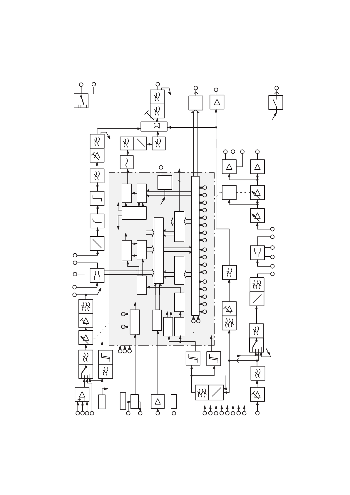
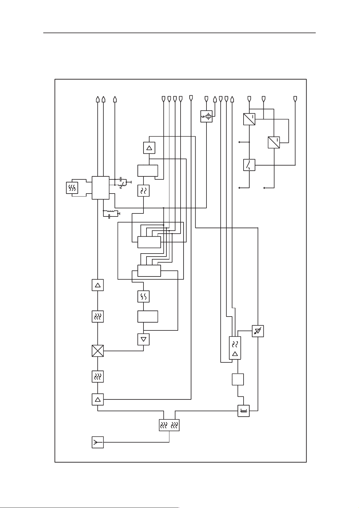
Block Diagram of System/RF Blocks (Version: 01; Edit: 89) 3A–1. .
Circuit Diagram of Connector (Version: 02; Edit: 89) 3A–2. . . . . . . .
Circuit Diagram of CTRLU Section (Version: 02; Edit: 119) 3A–3. . .
Circuit Diagram of PWRU Section (Version: 02; Edit: 101) 3A–4. . . .
Circuit Diagram of Audio Section (Version: 02; Edit: 228) 3A–5. . . . .
Circuit Diagram of Keyboard Section (Version: 02; Edit: 72) 3A–6. .
Circuit Diagram of Display Section (Version: 02; Edit: 18) 3A–7. . . .
Circuit Diagram of Receiver Section (Version: 02; Edit: 131) 3A–8. .
Circuit Diagram of Transmitter Section (Version: 02; Edit: 81) 3A–9.
Circuit Diagram of Synthesizer Section (Version: 02; Edit: 114) 3A–10
Layout Diagram (Version 01) 3A–11. . . . . . . . . . . . . . . . . . . . . . . . . . . . .
Original 11/97
Page 3 – 3
Page 4
NHN–6N
PAMS
System Module
Introduction
The baseband submodule controls the internal operation of the phone. It
controls the user interface, i.e. LCD driver, keyboard, and audio interface
functions. The module performs all signalling towards the system, and
carries out audio–frequency signal processing. In addition, it controls the
operation of the transceiver and stores tuning data for the phone.
All functional blocks of the baseband are mounted on a single multi layer
printed circuit board. This board also contains RF–parts. The chassis of
the radio unit contains separating walls for baseband and RF. All components of the baseband are surface mountable. They are reflow soldered .
The connections to the Display–module are fed through a flex to the
board connector.
The Baseband Module includes power supply, modem, audio filters, micro–controller, nonvolatile memory, SIS–processor, and keyboard. The
display is a separate module. Power supply circuits like regulators, voltage detection and charging control, are integrated to the custom MUUMI
circuit . The modem and audio operations are integrated into NIPA ASIC.
The micro–controller is a Hitachi H8 series controller with 64 kbytes ROM
and 2 kbytes RAM. The 2 kbytes EEPROM memory is of serial I
type. The SIS–processor is a Motorola MC68HC11A8 connected to the
controller over serial bus I2C.
Technical Documentation
2
C–bus
List of Sub–modules
Name of submodule Notes
CTRLU
PWRU
AUDIO
UIF
RECEIVER
TRANSMITTER
SYNTHESIZER
These blocks are only functional blocks and therefore have no type nor
material codes.
Control Unit for the phone
Power supply
Audio
User interface
Receiver
Transmitter
Synthesizer
Page 3 – 4
Original 11/97
Page 5
PAMS
NHN–6N
Technical Documentation
Modes of Operation
The module has three operating modes: stand–by, listening, and conversation mode.
Standby mode:
CPU‘s clock is switched off, only NIPA timer is running to take care of battery save timings.
If charger is connected CPU doesn‘t go to standby mode.
Listening mode:
In the listening mode, some blocks of the audio IC (NIPA) are in standby
state.
Conversation mode:
System Module
In the conversation mode all ICs are active.
DC Characteristics
Pin / Conn. Line Symbol Minimum Typical /
Nominal
VCS
VCS
VBA T 4.5V 4.8V 6.8V
VRF 4.5V 4.8V 6.8V VBAT for RF mod-
VA 3.1V 3.3V 3.5V Imax = 20mA
VL2 3.1V 3.3V 3.5V Imax = 40mA
VL3 3.84V 4.0V 4.16V Imax = 100mA
VREF 3.2V 3.3V 3.42V Imax = 5mA
9.5V 10.5V 10.5V LCH–6; ACH–6
740mA
10.5V 12.0V 16.5V ACH–8
265mA
Maximum Unit / Notes
ule
Original 11/97
Page 3 – 5
Page 6
NHN–6N
PAMS
System Module
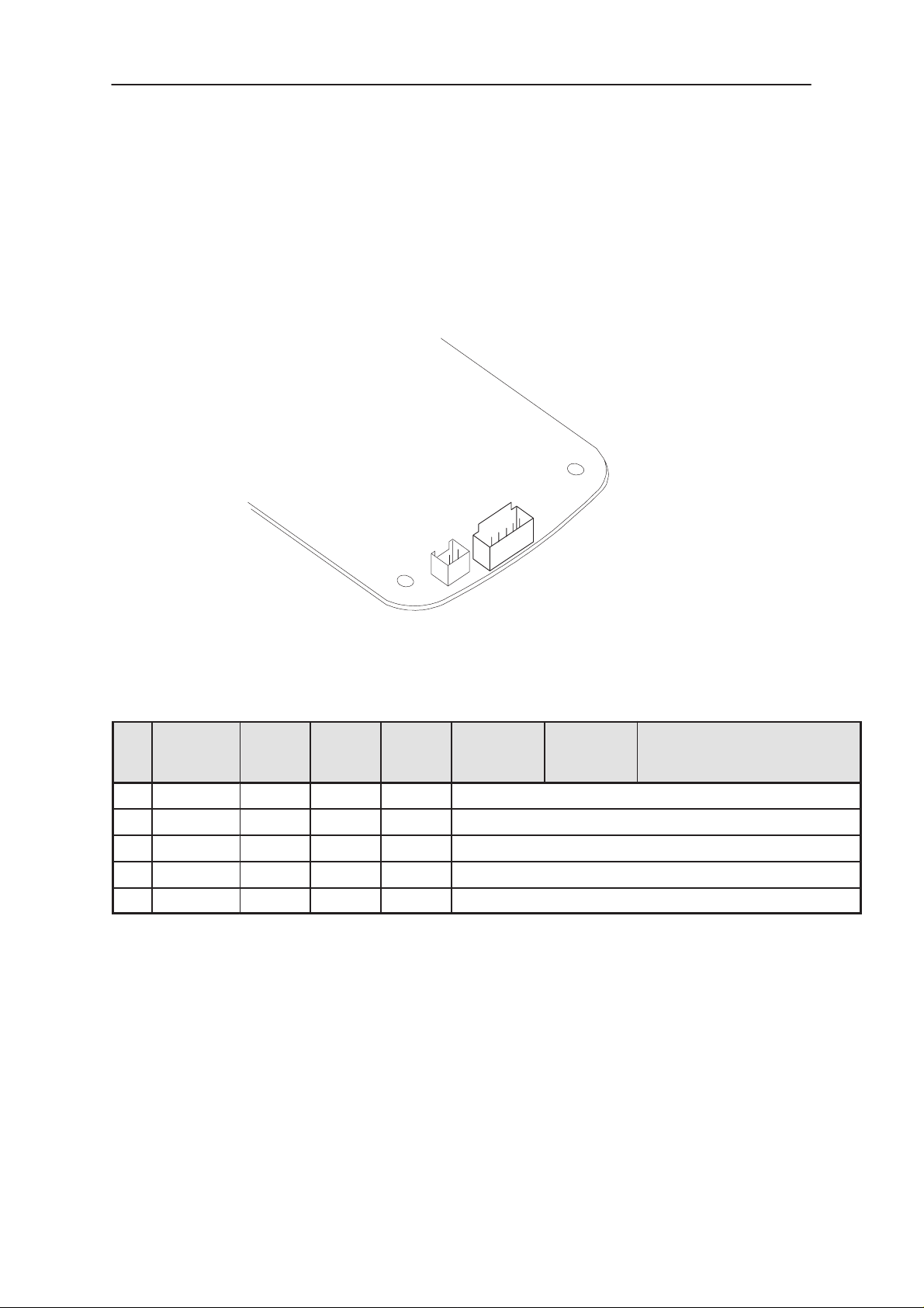
Connections
Battery/Service Connector
Technical Documentation
Pin Line
Symbol
1 VBAT 4.2V 4.8V 6.8V Battery voltage for transceiver.
2 MBUS Mbus line
3 XEAR External earphone
4 XMIC External microphone
5 GND Power supply ground.
Mini-
mum
Typical
/ Nomi-
nal
Maxi-
mum
Minimum Typical /
Nominal
Maximum
Page 3 – 6
Original 11/97
Page 7
PAMS
NHN–6N
Technical Documentation
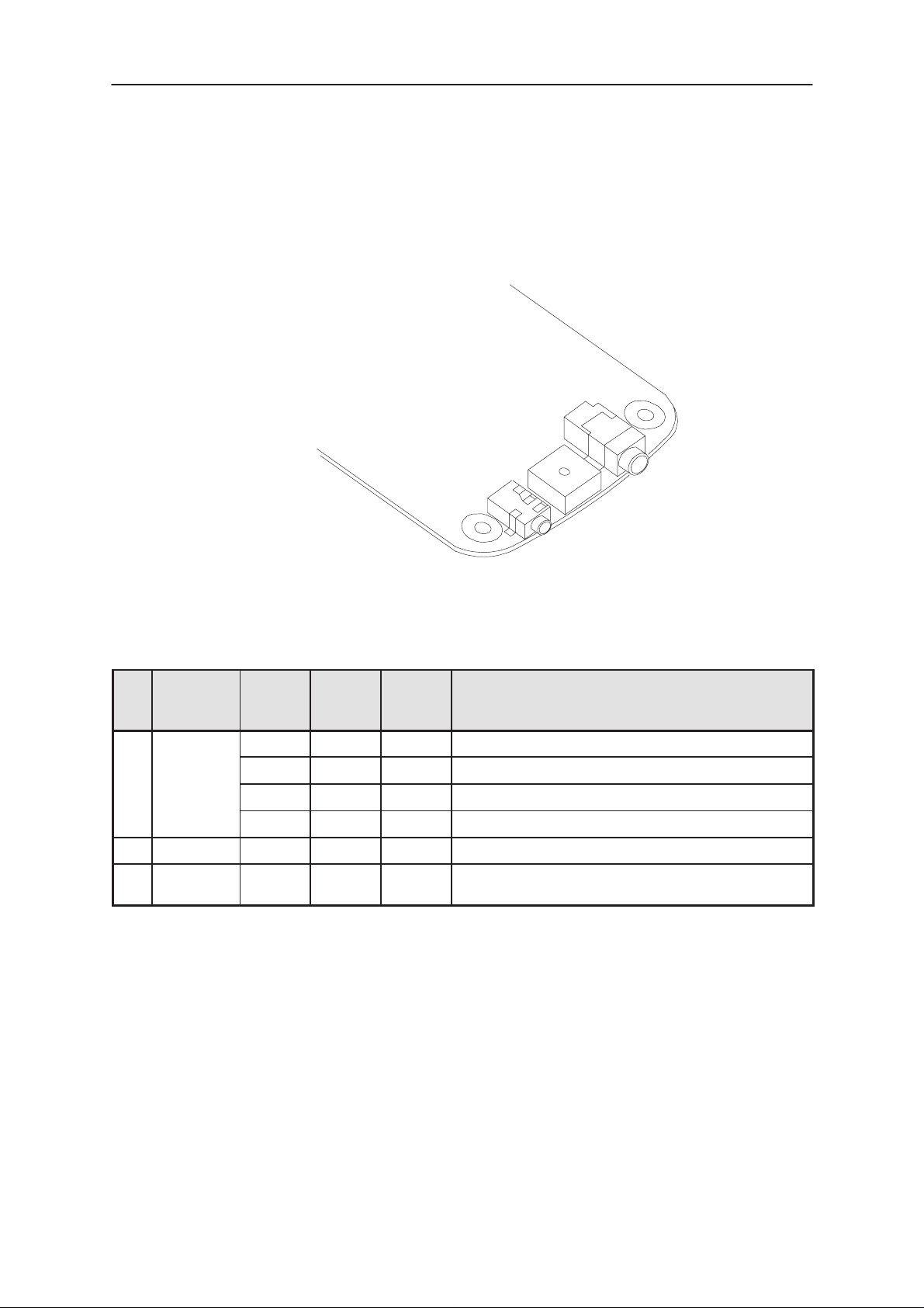
Charger Connector
System Module
Pin Line
Symbol
2 VCS
3 GND Power Supply Ground
4 TERMI-
NAL
Minimum
9.5V 10.5V 10.5V LCH–6 and ACH–6
10.5V 12.0V 16.5V ACH–8
Typical
/ Nomi-
nal
740mA
265mA
Maxi-
mum
Unit / Notes
S0001227
Original 11/97
Page 3 – 7
Page 8
NHN–6N
PAMS
System Module
Technical Documentation
Audio Specifications
Typical / Nomi-
nal
MIC (NIPA ’s input pin) 0.25 mV Mic amplifier input
EARP, EARM 760 mV Earphone amplifier output
XEAR 170mV
XMIC 260mV
rms
rms
Maximum Unit / Notes
(NIPA’s input pin)
Via Battery / Service
Connector
2600mV
rms
Via Battery / Service
Connector
Headset Connector
The handsfree headset is connected by a 2,5 mm TC – Jack. The external earphone and microphone use the same audio lines and the same
amplifier as the internal earphone and microphone.
Pin Line
Symbol
1 GND Power Supply Ground
Unit / Notes
2 XMIC Bias from NIPA, external microphone
3 XEAR Audio from amplifier, external earphone
4 MIC Internal microphone
5 EAR Internal earphone
Page 3 – 8
Original 11/97
Page 9
PAMS
NHN–6N
Technical Documentation
System Module
Circuit Description
CTRLU
The Control block controls all phone functions, and SIS–processor too.
CTRLU Internal Signals, Inputs
Signal Name Notes From
VL2 Logic supply voltage Max 40 mA PWRU
VL3 SIS processor and earphone amplifier supply voltage PWRU
VREF Reference voltage 3.3V 2%. Max. 5mA. PWRU
PWRON Signal from power button. PWRU
XRES Reset line from MUUMI PWRU
VCHARG Charger voltage to A/D converter PWRU
VBATSW Battery voltage to A/D converter . PWRU
BTEMP Battery temperature CTRLU
RFTEMP RF temperature SYNTHESIZER
RSSI Received signal strenght indication RECEIVER
TXI Transmitter output power level indication TRANSMITTER
RXD Serial interface (M2BUS) PWRU
XINT Interrupt request from NIPA AUDIO
NMI No maskable Interrupt request from NIPA AUDIO
CLKMCU Clock for controller AUDIO
HSCONN Headset recognition AUDIO
CTRLU Internal Signals, Outputs
Signal Name Notes To
TXD Serial interface (M2BUS) PWRU
CSW Charger control PWRU
AGC Gain control RECEIVER
RXE RX Circuit power on/off RECEIVER
SCLK Synchronous data clock for synthesizers SYNTHESIZER
SDAT Synchronous data for synthesizers SYNTHESIZER
SLE Synthesizer data latch enable SYNTHESIZER
TXE Transmitter control (on/off) TRANSMITTER
TXC Transmitter Power Control TRANSMITTER
TXS TX synthesizer enable SYNTHESIZER
EAREN Earphone enable AUDIO
XNCS NIPA chip select signal AUDIO
XNWR NIPA write control signal AUDIO
Original 11/97
Page 3 – 9
Page 10
NHN–6N
PAMS
System Module
XNRD NIPA read control signal AUDIO
NA(3:0) NIPA address bus AUDIO
ND(7:0) NIPA data bus AUDIO
LIGHTS Backlights on/off UIF
COL0/
XPWROFF
COL1–4 Lines for keyboard read (keypad outputs) UIF
ROW0–2 Lines for keyboard read (keypad inputs). Input pullup used UIF
LCDD0–3 Lcd driver data UIF
E Lcd driver chip select signal UIF
RW Lcd driver read/write select signal UIF
RS Lcd driver register select signal UIF
LCDRES Lcd driver reset signal UIF
MBUSEN Mbus enable AUDIO
Line for keyboard read/
Power off control
Technical Documentation
UIF
ToNotesSignal Name
Block description
CTRLU – PWRU
CTRLU controls the watchdog timer in MUUMI. It sends a positive pulse
at approximately 1 s intervals to the XPWROFF pin of MUUMI to keep the
power on. If CTRLU fails to deliver this pulse, the MUUMI will cut off power from the system. CTRLU also controls the charger on/off switching in
the PWRU block. When power off is requested, CTRLU leaves the
MUUMI watchdog without reset. After the watchdog has elapsed, MUUMI
cuts off the supply voltages from the phone. Battery charging is controlled
by CSW line, which is a PWM–controlled output port (frequency about 11
Hz).
VBATSW, Battery voltage measurement
The battery voltage can be measured up to 9.075 V nominal with 3.3 V
reference voltage. The absolute accuracy is low because of the reference
3 % accuracy, and A/D–converter +/– 8 LSB accuracy . This battery voltage measurement offset error must be calibrated with input voltage 4.8 V.
The A/D conversion result can be calculated from the equation:
A/D readout = 1024 * (VBATSW* ( 4/11)) / VREF VREF=3.3V
Page 3 – 10
For example:
6.9 V results 778 = 30AH
4.8 V results 542 = 21EH
4.0 V results 451 = 1C3H
Original 11/97
Page 11

PAMS
NHN–6N
Technical Documentation
VCHARG, Charger voltage measurement
The charger voltage can be measured up to 21.6 V nominal. The
A/D–conversion result can be calculated from the equation :
A/D readout = 1024 * (VCSW*(18/118)) / VREF VREF=3.3 V
For example:
BTEMP , Battery temperature measurement
Battery temperature measurement is implemented with 15 kohm NTC
and 47 kohm pull–up resistor. The A/D conversion readout can be calculated from the equation:
11 V gives 520 = 208H
10 V gives 473 = 1D9H
4.8 V gives 227 = 0E3H
A/D readout= 1024* ( R
NTC
/( R
NTC
System Module
+47k))
CTRLU – AUDIO
The interface between micro–controller and NIPA circuit is a bi–directional
8–bit data bus with 4 address lines. Address, data, and control lines are
used in micro–controller as I/O–port pins. Data line direction must be controlled with the micro–controller data direction register. The Interface includes address outputs NA0–3, data inputs (read) / outputs (write)
ND0–7, chip select control output XNCS, read control output XNRD, write
control output XNWR, and interrupt inputs XINT and NMI. To minimize
power consumption in battery stand by mode, control signals XRD and
XCS should be in ’0’ state, address output NA0–3 and NWR in ’1’ state,
and data lines ND0–7 should be inputs .
CTRLU – UIF
The keyboard is connected directly to the controller. COL0–4 are output
lines and ROW0–2 are input lines. The watchdog is updated at the same
time as keyboard scanning (XPWROFF). Keyboard scanning is done by
driving one COL to 0 V at time, and ROWs are used to read which key is
pressed.
For example:
+25°C gives 247 = 0F7H ( About 0.8 V )
The keyboard and LCD lights are controlled by the LIGHTS signal.
The LCD controller interface to the micro–controller are 4 bi–directional
data lines DD0–3, register select control RS output, read/write control RW
output, and bus enable control E output. The data lines LCDD0–3 and
control signals RS, RW must be set to high state during standby opera-
Original 11/97
Page 3 – 11
Page 12

NHN–6N
PAMS
System Module
tion because of the pull–up resistors in the LCD controller. LCD controller
resetting requires clock signal during XRES active low which is controlled
by LCDRES line. The MCU disables LCDRES after it has set LCDCLK
frequency to 57.6 kHz.
CTRLU – RECEIVER
The RECEIVER circuit power is connected on/off by the RXE signal.
Received signal strength is measured over the RSSI line, and the inter-
mediate frequency is measured over the IF line.
CTRLU – SYNT
The frequency is controlled by the AFC signal. The synthesizer is controlled via the synchronous serial bus SDAT/SCLK. The data is latched to
the synthesizer by the positive edge of the SLE line. The TX synthesizer
power on/off (TXS) line is controlled via PLL circuit. Control information is
programmed by using the SDAT line.
Technical Documentation
RFTEMP, RF temperature measurement
RF temperature measurement is implemented with 15 kohm NTC and
47 kohm pull–up resistor. The A/D conversion readout can be calculated
from the equation:
A/D readout= 1024* ( R
For example:
25 C gives 247 = 0F7H ( about 0.8 V )
CTRLU – TRANSMITTER
The transmitter output power level is measured over the TXI line. The
TXE line activates the power module. The power is controlled via the TXC
line which is a PWM–controlled output port (frequency about 5.1 kHz).
Main components
H8/3032 is a CMOS micro–controller. All memory needed (64kB ROM,
2kB RAM) except the EEPROM, is located in the controller. The MCU operating clock (3.6864 MHz) is generated on NIPA. H8/3032 is operating in
single–chip normal mode (mode 2) 64 kbyte address space, so all input/
output pins are used as I/O–ports.
NTC
/( R
NTC
+47k))
Pin Number Port Signal Description
1 PB0 SDAT
2 PB1
3 PB2
4 PB3 RXD
Page 3 – 12
Serial data for synthesizer
M2BUS net free timer input
Original 11/97
Page 13
PAMS
NHN–6N
Technical Documentation
5 PB4 EAREN
6 PB5 LCDRES
7 PB6 PWRON
8 PB7 SLE
9 P90 TXD
10 P92 RXD
11 P94 ECLK
12 VSS GND
13 – 20 P30 – P37 ND0 – ND7
21 VCC VL2
22 P10 NA0
23 P11 NA1
System Module
DescriptionSignalPortPin Number
Earphone enable
Reset for Lcd driver
Power button state
RX/TX synthesizer latch
Serial interface (M2BUS)
Serial interface (M2BUS)
Serial clock for EEPROM
Parallel data bus for NIPA
Address line for NIPA
Address line for NIPA
24 P12 NA2
25 P13 NA3
26 P14 XNCS
27 P15 XNWR
28 P16 XNRD
29 P17 LIGHTS
30 VSS GND
31 – 34 P20 – P23 LCDD0 – LCDD3
35 – 37 P24 – P26 ROW0 – ROW2
38 P27 COL4
39 P50 COL0/XPWROFF
40 – 42 P51 – P53 COL1 – COL3
43 P60 TXS
Address line for NIPA
Address line for NIPA
NIPA chip select
Read/write control to NIPA
Read/write control to NIPA
Backlight control
Lcd driver data
Keypad inputs (Input pullup
used)
Keypad output
Keypad output /
Watchdog control
(XPWROFF)
Keypad outputs
TX synthesizer enable. Ac-
tive high
44 – 45 MD0 – MD1
46
47 STBY
48 RES XRES
49 NMI NMI
50 VSS GND
NC
Original 11/97
Mode selection
Reset from MUUMI
Interrupt request from
NIPA
Page 3 – 13
Page 14
NHN–6N
PAMS
System Module
51 EXTAL CLKMCU
52 XTAL
53 VCC VL2
54 P63 TXE
55 P64 AGC
56 P65 RXE
57 RESO
58 AVSS GND
59 P70 VBATSW
60 P71 VCHARG
61 P72 RSSI
Technical Documentation
DescriptionSignalPortPin Number
External system clock from
NIPA
Transmitter on/off
Receiver gain control
RX circuit power on/off
Battery voltage
Charger voltage
Received signal strength
62 P73 TXI
63 P74 BTEMP
64 P75 HSCONN
65 P76 RFTEMP
66 P77
67 VREF VREF
68 AVCC VREF
69 P80 XINT
70 P81 RS
71 P82 RW
72 P83 E
73 PA0 SISCLK
74 PA1 SISD
Transmitter power monitor
Battery temperature
Headset recognition
RF temperature
Interrupt request from
NIPA
Lcd driver register select
Lcd driver read/write
Lcd driver chip select
Serial clock for SIS–pro-
cessor
Serial data for SIS–proces-
sor
75 PA2 EDATA
76 PA3 SCLK
77 PA4 CSW
78 PA5 MBUSEN
79 PA6 TXC
80 PA7
Page 3 – 14
Serial data to/from EEPROM
Serial clock for synthesizer
Charging control
Mbus enable
Transmitter power control
Original 11/97
Page 15
PAMS
NHN–6N
Technical Documentation
MC68HC11A8
MC68HC11A8 is a SIS (subscriber identification) circuit connected to the
controller over serial bus I2C.
SIS–processor signals
Pin No Signal From
31 EXTAL Clock input from the NIPA
43 RESET Reset input
47 PD0
50 PD1
EEPROM
I2C bus clock
I2C bus data
There is one 2k EEPROM in the phone. EEPROM is a nonvolatile
memory into which the tuning data for the phone is stored. In addition, it
contains the short code memory locations to retain user selectable phone
numbers.
System Module
EEPROM signals
Pin No Signal Description
5 SDA
6 SCL
I2C bus data
I2C bus clock
Original 11/97
Page 3 – 15
Page 16
NHN–6N
PAMS
System Module
Technical Documentation
PWRU
The power block provides the supply voltages for the baseband, and also
includes the charging electronics.
PWRU Internal Signals, Inputs
Signal Name Notes From
VBAT Battery voltage input CONNECTOR
XPWRON Power on control from keyboard UIF
XPWROFF Power off control from controller (watch dog) CTRLU
VCS Charging supply voltage from charger CONNECTOR
CSW Charger control CTRLU
TXD Serial interface (M2BUS) CTRLU
M2BUS Serial interface CONNECTOR
PWRU Internal Signals, Outputs
Signal Name Signal description To
VA Analog supply voltage. Max 20 mA. AUDIO
VL2 MCU supply voltage CTRLU, UIF
VL3 SIS processor and earphone amplifier supply voltage CTRLU, AUDIO
VREF Reference voltage 3.3V 2%. Max. 5mA. CTRLU, PWRU
RECEIVER,
TRANSMITTER
XRES Master reset CTRLU, AUDIO
VBATSW Battery voltage to A/D converter . CTRLU
VCHARG Charger voltage to A/D converter CTRLU
RXD Serial interface (M2BUS) CTRLU
PWRON Power button indicator, PWRON is same as XPWRON but
buffered and inverted.
CTRLU
Block description
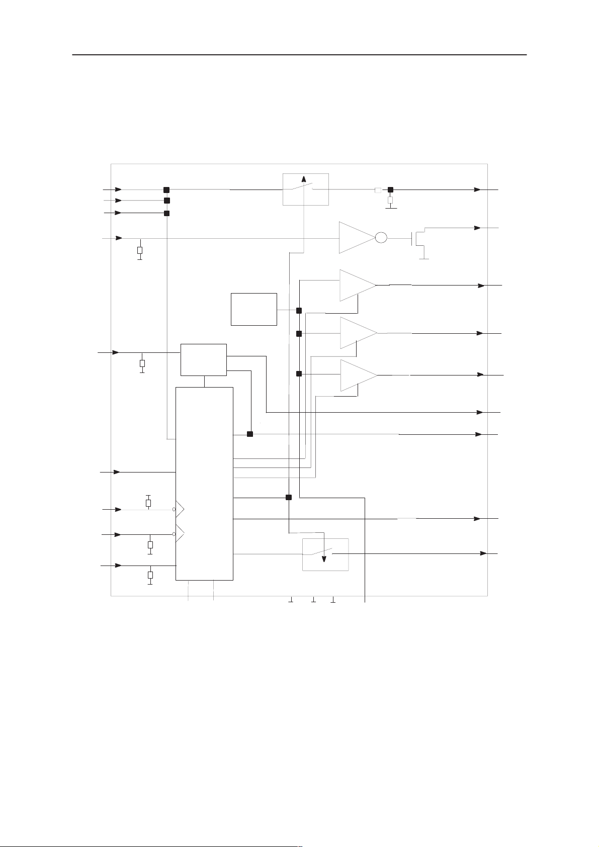
The baseband power supplying circuit MUUMI includes:
– the supply voltages:
VL2 40mA for digital circuits
VA 20mA for analog circuits
VREF 5mA reference voltage for A/D–converters and
regulators
– the supply voltage VL3 (100mA) for SIS–processor and earphone amplifier is generated by external regulator
– switched output of battery (VBATSW) and charger voltage (VCHARG)
measurements to MCU A/D–converter
– battery voltage detection and reset logic
– charger switch control output used to limit battery voltage VBAT < 6.8V
– power on/off switch input (XPWRON), buffered output to MCU
Page 3 – 16
Original 11/97
Page 17

PAMS
NHN–6N
Technical Documentation
(PWRON)
– watchdog timer using oscillator in COFF pin , cleared by falling edge
input in PWROFFX, elapsing time for watchdog timer is 3 ... 4 seconds
– M2BUS open drain output driver.
The charge switch driving circuit is implemented with discrete components. This circuit includes transient voltage protection, soft charge
switching, low voltage battery charging and battery disconnecting with
charger connected protection. This circuit also limits battery voltage when
charger is connected to protect MUUMI and TX transistors.
Power circuitry have three different operating modes: POWER OFF , RESET and POWER ON. In POWER OFF state MUUMI regulator outputs
are disabled and reset control output signal (PURX) is active low.
MUUMI internal oscillator at pin COFF is working in all operating modes.
MUUMI goes through short RESET state (100ms ) to POWER ON–state
, if PWR–button is pressed or charger voltage input is connected to
charging input VCS (charging voltage detection in MUUMI input VCHAR
is level active). In RESET–state regulator outputs VL,VA and VREF are
active and PURX–signal is active low. If battery voltage VBAT is lower
than 4.1 V (3.9V...4.3V) the circuit cannot go to POWER ON state.
MUUMI goes also to RESET state, when battery voltage is falling below
3.9 V (3.7V...4.1V). This situation is possible, when battery is fully discharged or battery is disconnected.
System Module
In POWER ON mode all regulator outputs are active and MUUMI reset
signal output PURX is inactive high. Micro–controller XPWROFF–output
signal clears at falling edge the watchdog inside MUUMI. If the watchdog
is not cleared , MUUMI goes to POWER OFF state. When the charger is
connected and battery voltage is higher than 4.1V , module stays in
POWER ON mode.
The micro–controller controls battery charging with CSW output (which is
PWM–controlled output port) and MUUMI limits the maximum battery voltage to 6.8 V with CHRGSW–output.
No current flows from charger (VCHARG) to battery , if MCU output CSW
is active low and XRES signal is inactive high. The battery is charged
also, when charger is connected and XRES signal is active low. The
charging circuit charges the battery during RESET to higher than 4.3 V.
The charging electronics is controlled by the CTRLU. When the charging
voltage is applied to the phone while the phone is powered up, the
CTRLU detects it and starts controlling the charging.
If the phone is in power–off, the MUUMI will detect the charging voltage .
If the battery voltage is high enough the reset will be released and the
CTRLU will start controlling the charging. If the battery voltage is too low
the phone is in reset and charging control circuitry will pass the charging
current to the battery. When the battery voltage has reached 4.1V
(3.9...4.3V) the reset will be removed and the CTRLU starts controlling
the charging. This all is invisible to the user.
Original 11/97
Page 3 – 17
Page 18

NHN–6N
PAMS
System Module
V116 is the charging switch; it is governed by the controller (CSW line) via
voltage regulator V114 and V115. In fast charge mode CSW is ”1” and in
maintain charge mode there is controller controlled pulses. In charge off
state CSW is ”0”. In maintain charge mode pulse ratio depends of charger
and temperature.
There is three different ways to switch power on:
– Power key pressing grounds the XPWRON line. The MUUMI defects
that and switches the power on.
– Charger detection on MUUMI detects that charger is connected and
switches power on.
– MUUMI will switch power on when the battery is connected. If the bat-
tery is changed during the call, the power is kept on. If not the power
is switched off.
Technical Documentation
Page 3 – 18
Original 11/97
Page 19
PAMS
NHN–6N
Technical Documentation
MUUMI Block diagram
VBAT1
1
VBAT2
22
VBAT3
5
M2BUSIN
11
760k
PWM
15
760k
CHARGER
CTRL
LOGIC
BANDGAP
REF
70k
40k
System Module
VBATSW
M2BUSOUT
VL2
VA
VREF
17
12
23
2
4
21
13
14
3
VCHAR
PWRONX
PWROFFX
TEST
VBAT
32k
760k
760k
LOW VBAT
& CHARGER
DETECT
PWR ON/OFF
&
RESET LOGIC
Creset
20
16
Coff
VL_ENA
VA_ENA
VREF_ENA
VSW_ENA
VCHAR
GND1
24
GND2
19
GND3
7
CHRGSW
PWRONXBUFF
VCHARSW
Cref
6
PURX
8
10
9
18
Original 11/97
Page 3 – 19
Page 20

NHN–6N
PAMS
System Module
AUDIO
Introduction
The block includes NIPA audio/signalling processor in a 64 TQFP package for NMT450 and NMT900 systems.
Main features
– Single chip FFSK modem and audio circuit
– Full duplex 1200 baud signalling
– DMS facility
– Low power consumption modes
– Programmable output clocks with clock stop for MCU and LCD
– 8 bit parallel interface with pull ups
– FSK indicator and level detector
– Speech volume indicator
– Programmable timer
– IF counter
– 8 bit DAC
– FII filter and gain control
– Low noise microphone amplifier
– Input for a handset microphone or an accessory
– Microphone sensitivity compensation +4.8/–4.2 dB range (4 bits)
– Compander
– RX and TX filters
– Tx hard limiter
– Tx AGC
– Internal reference compensation +1.00/–0.75 dB range(3 bits)
– Summing stage for voice/data, signalling and fii
– Transmitter compensation amplifier with +3.75/–3.75 dB range (4 bits)
– Receiver compensation amplifier with +3.75/–3.75 dB range (4 bits)
– Volume control amplifier with –20/+17.5 range (4 bits)
– Earphone amplifier with drive capability for ceramic earpiece
– Buffered output for a handset or an accessory
– Mute switches
– Dual and single tone multi–frequency generator
– Driver for buzzer amplifier
– Hands free functions
Technical Documentation
Page 3 – 20
Original 11/97
Page 21
PAMS
NHN–6N
Technical Documentation
System Module
Technical specifications
AUDIO Internal Signals, Inputs
Signal Name Notes From
XRES Reset line from MUUMI PWRU
XNCS Chip select signal CTRLU
XNWR Write control signal CTRLU
XNRD Read control signal CTRLU
NA0...3 4–bit address bus CTRLU
ND0...7 8–bit bi–directional data bus CTRLU
EAREN Earphone enable CTRLU
MBUSINT M2BUS interrupt request PWRU
KBINT Keyboard interrupt request UIF
IF (2nd) Intermediate frequency for AFC function RECEIVER
DAF Detected audio signal from receiver RECEIVER
XMIC External audio input from service accessories CONNECTOR
VBAT Battery voltage CONNECTOR
VA Analog supply voltage Max 20 mA. PWRU
VL3 Logic supply voltage for earphone amplifier, Max 100mA PWRU
MBUSEN Mbus enable from CTRLU CTRLU
AUDIO Internal Signals, Outputs
Signal Name Notes To
XINT Interrupt request to MCU CTRLU
NMI No maskable Interrupt request to MCU CTRLU
HSCONN Headset recognition to CTRLU CTRLU
LCDCLK Clock signal for LCD driver ( 57.6 kHz) UIF
CLKMCU Clock signal for MCU (3.6864 MHz) CTRLU
XEAR External audio output to service accessories CONNECTOR
MOD Audio output to synthesizer SYNTHESIZER
AFC VCTCXO control SYNTHESIZER
NIPA Pin list
Pin no Symbol Pin type Notes
1 VDD1 + 3.3 V Supply voltage, digital
2 XRD DIN/pd Read control signal, active state LOW, pull–down > 50
k
3 XCS DIN/pd Chip select signal, active state LOW, pull–down > 50
k
Original 11/97
Page 3 – 21
Page 22

NHN–6N
PAMS
System Module
NotesPin typeSymbolPin no
4 A3 DIN/pu 4–bit address bus, MSB, pull–up > 50 k
5 A2 DIN/pu 4–bit address bus, pull–up > 50 k
6 A1 DIN/pu 4–bit address bus, pull–up > 50 k
7 A0 DIN/pu 4–bit address bus, LSB, pull–up > 50 k
8 D7 DIO 8–bit bi–directional data bus MSB
9 D6 DIO 8–bit bi–directional data bus
10 D5 DIO 8–bit bi–directional data bus
11 D4 DIO 8–bit bi–directional data bus
12 D3 DIO 8–bit bi–directional data bus
13 D2 DIO 8–bit bi–directional data bus
14 D1 DIO 8–bit bi–directional data bus
15 D0 DIO 8–bit bi–directional data bus LSB
16 VDD2 + 3.3 V Supply voltage, digital
Technical Documentation
17 NMI DOUT Non maskable Interrupt request
18 XCLR DIN HW reset input, active state LOW
19 TMODE DIN/pd Test mode selection, pull–down > 50 k
20 TSEL DIN/pd Test select, pull–down > 50 k
21 XINT DOUT Interrupt request to MCU, active state LOW
22 MBUSINT DIN MBUS interrupt request, falling edge active
23 KBINT DIN Keyboard interrupt request, falling edge active
24 IF AIN IF input
25 VSS2 0 V Supply voltage, digital ground
26 VSA2 0 V Supply voltage, analog ground
27 DAF AIN Signal input
28 FILO AOUT Rxfilter output
29 EXPI AIN Expander input
30 EAMPBO AOUT Expander Amplifier B output
31 EWCI AIN Expander Window Comparator input
32 EXPO AOUT Expander output
33 VDA2 + 3.3 V Supply voltage, analog
34 VOLI AIN Volume control ampl. input (Volume)
35 EXTEAR AOUT Buffered output for handset or an accessory
36 EVGND AIN Earphone driver virtual ground
37 EARM AOUT Earphone driver output
38 EARP AOUT Earphone driver output
39 EARFB AIN Pin for feedback resistor of EARphone amplifier
40 DACO AOUT DA converter output
Page 3 – 22
Original 11/97
Page 23
PAMS
NHN–6N
Technical Documentation
NotesPin typeSymbolPin no
41 EARIN AOUT Pin for input resistor of EARphone amplifier
42 REF AIN Internal analog signal ground 1.65 V
43 MIC AIN Microphone amplifier input
44 BIMIC AOUT Microphone bias current output
45 CMIC AIN Microphone current stabilization capacitor
46 EXTMIC AIN Audio input for a handset or an accessory
47 TXBPO AOUT Transmit bandpass filter output
48 VDA1 + 3.3 V Supply voltage, analog
49 COMI AIN Compressor input
50 COMO AOUT Compressor output
51 EMPI AIN Pre emphasis input
52 FIIOUT AOUT Received FII signal
53 TOUT DOUT Test output, digital
System Module
54 ATST AOUT Audio Filter Test output
55 MOD AOUT Transmit path output
56 VSA1 0 V Supply voltage, analog ground
57 VSS1 0 V Supply voltage, digital ground
58 BUZZ DOUT Buzzer output
59 ATOUT AOUT Test pin
60 CLKIN CIN 7.3728 MHz (3.6864 MHz) crystal oscillator input or
input for the external clock
61 CLKOUT COUT 7.3728 MHz (3.6864 MHz) crystal oscillator output
62 CLKLCD DOUT Clock signal for LCD, 230.4 kHz or 57.6 kHz
63 CLKMCU DOUT Clock signal for MCU, 3.6864 MHz or 7.3728 MHz
64 XWR DIN/pu Write control signal, active state LOW, pull–up > 50
k
Original 11/97
Page 3 – 23
Page 24
NHN–6N
R
PAMS
System Module
NIPA Block Diagram
ATST
ATOUT
LIM
TXAAF
PREEMP
EMPI
CWCI
COMI COMO
TXBPO
AGC
VOL
SUM
TXTRI
RXAAF
SINGEN
MODTRFIL
MODRXFIL
TXLP TXTRI+TXPOSTFIL
AGC
PREEM LIM
COMPR
DATACOMP
txbpo
(to SIDEAR)
aloop (to RXMUX)
SINGEN MODTRFIL
FSKMOD
TRSTBY
TR
RFLAG
TFLAG
RECCTRL
INTERNAL
WTRFIL
SUM
TRREG
CTRL
STATUS
BITS
RECREG
DPLL
CLOCKS
MOD
WPOSFIL
ddtmf
SMUX
loop (to MODRXFIL)
MODTRPOST
BUZZ
DRIV
BUZZ
CONTROL BITS
DFLAG
DETED
AFC
XBSSBY
XTALKSBY
XBUZZSBY
XIFSBY
CREG
TIMER
DETFIL
DACO
D/A
8 bit
XDACSBY
XDTMFSBY
INTERFACE
FIIBUF
A0 A1 A2 A3 D0 D1 D2 D3 D4 D5 D6 D7
NMI
XINT
XWR
XRD
XCS
Technical Documentation
FIIOUT
EAR
FIIPOST
EARP
HF
EARM
CONTR
EVGND
RXATT ACC
EXP VOL
DEEMP+RXFIL
EXTEAR
SIDEA
SIDEAR
txbpo
(from TXBP)
64 pins
VOLI
EXPO
EWCI
EAMPBO
EXPI
FILO
MICAM
Page 3 – 24
TXMUX+TXAAF TXATT MICTRI TXBP
MIC
CMIC
BIMIC
ddtmf (to BUZZDRIV)
DTMFCOMP
dtmf
DTMF GEN
EXTMIC
CLKLCD CLKMCU
XCLR
TMODE
(to RXMUX)
REF GEN
CLKIN
CLOCKDIV
TSEL
OSC
IFAMP
CLKOUT
IFCNTR
IF
FSKIND
GND GEN
REF
FSKDIS
DATACOMP
KBINT
MBUSINT
MODRXFIL
LEVEL
FSKLEV
VDD2
VDD1
FIIFIL(4kHz)+FIITRI
dtmf
loop (from WPOSFIL)
VSS2
VSA1
VDA1
VDA2
RXMUX+AAFIL
VSA2
VSS1
aloop (from TXPOSTFIL)
RXTRI RXAAF
DAF
Original 11/97
Page 25

PAMS
NHN–6N
Technical Documentation
Transmit (TX) audio signal path
The TX audio signal is processed in the NIPA circuit and fed via the MOD
line to the TX synthesizer on SYNTHESIZER module.
NIPA ASIC contains the following stages for TX signal processing:
MICAM:
The signal from the microphone is fed to this stage and amplified up to
200 mVrms.
TXMUX + TXAAF:
TX source selection (exmic/mic/dmmf/muted). Txaafil prevents aliasing in
TXBP filter.
TXATT:
TXATT is a hands free attenuator. Maximum attenuation is selectable
from four levels: –30, –27, –24 or –21 dB.
MICTRI:
System Module
MICTRI is for different microphone (phone microphone, headset and
handset etc.) sensitivity compensation. It is used also for dtmf level setting. Gain 16 levels, step 0.6 dB.
BANDPASS:
Tx bandpass filter takes out high freq noise and low freq hum.
COMPR:
It compresses speech dynamic area to avoid noise at tx and radio path. It
is an amplitude compressor and ratio is 2:1 in dB scale. It can be bypassed for measurement or dtmf purposes.
PREEMP:
Pre–emphasis filter gives +6 dB/oct emphasis.
AGC:
A soft limiter is needed in order to suppress inter–modulation. Signal
measuring circuitry measures peak–to–peak voltage. If the signal on soft
limiter input is not a sine signal (clipped in preceding stages), peak–to–
peak signal level is increased in the post limiter filter.
LIM:
Hard limiter. It cuts the signal transients to 1131 mVpp levels.
TXLP:
The corner frequency of tx lowpass filter is 3400 Hz. Amplitude attenua-
tion is 12 dB/oct after the corner point. Filter includes notch at 4 kHz.
TXTRI:
TXTRI is for nominal deviation tuning. Gain 8 levels, step 0.5 dB.
TXPOSTFIL:
Original 11/97
Page 3 – 25
Page 26

NHN–6N
PAMS
System Module
Postfil eliminates filter clock.
SUM:
Speech, data and FII signals are summed together.
WTRFIL:
This block is a lowpass filter for FII and data. Transmitter Compensation
Amplifier is these too. Gain 16 levels, step 0.5 dB.
WPOSFIL:
WPOSFIL filters out the replicates of the output spectrum around WTRFIL
clock frequency and its harmonics.
RECEIVE (RX) AUDIO SIGNAL PATH
Technical Documentation
NIPA contains the following stages for RX signal processing:
RXTRI:
RXTRI is for demodulation sensitivity compensation. Gain 16 levels, step
0.5 dB.
RXAAF:
RX aafilter filters out noise and other high frequency components from
the incoming signal. It prevents aliasing in FIIFIL, RXFIL and MODRXFIL.
RXMUX+AAFIL:
Rxmux selects speech from DAF–pin or DTMF from generator or a loop
from TXTRI or mute. Aafil prevents aliasing in RXFIL.
DEEMP+ RXFIL:
Rx filter filters out high freq noise and low freq hum. It has de–emphasis
–6 dB/oct for the received speech signal. Design should include notch at
4kHz.
EXP:
It expands speech dynamic back to normal. It is an amplitude expander
and ratio is 1:2 in dB scale. It can be by–passed for measurement or dtmf
purposes.
VOL:
VOL is for earphone or accessory speaker/earphone volume control. Vol-
ume Control Amplifier. Gain 16 levels over –20 to +17.5 dB in 2.5 dB
steps.
Page 3 – 26
Original 11/97
Page 27

PAMS
NHN–6N
Technical Documentation
RXATT:
RXATT is a hands free attenuator. Maximum attenuation is selectable
from four levels: –30, –27, –24 or –21 dB.
Hands free controller (HF CONTR) measures peak–to–peak level of the
received audio and controls gains of the transmit and receive attenuators
as a function of measured signal level.
EAR:
The Earphone Amplifier is a single input, differential output amplifier for a
ceramic earpiece.
ACC:
Buffer for accessory line is capable of driving high capacitive load. Gain
and response of the buffer are fixed.
Transmitting data path
The data to be transmitted will be loaded into the transmitting register
TRREG. From the TRREG register the 8 bit data is transformed to serial data
which is sent to the FSK modulator (FSKMOD) and sine wave generator
(SINGEN) and then to the summing block (SUM).
System Module
Receiving data path
The data from anti alias filter is connected through the modems RX filter
(MODRXFIL) to the data comparator (DA TACOMP) and then to FSK discriminator. Further from FSK discriminator data is connected to detecting filter
(DETFIL) and from there to digital phase locked loop (DPLL).
IF
Intermediate frequency counter (IFCTR) is on the modem to measure
the frequency of IF signal.
AFC
AFC provides the synthesizer fine tuning. It can also be used for channel
sidestep.
AFC DA–converter output DC level tunes RF oscillator (VCXO).
FII path
The FII signal is filtered and amplified with a 4 kHz bandpass filter (FIIFIL). FIITRI is for FII sensitivity compensation. The filtered FII is then fed to
the summing block (SUM).
Original 11/97
Page 3 – 27
Page 28

NHN–6N
PAMS
System Module
Buzzer driver
The buzzer driver is a ’semi PWM’ signal generator. It detects rising edges
of DTMF signal and generates a pulse on every rising edge. The length of
the pulse can be set by writing a length control word to the register BUZZVOL. The length is N * 2.17 us, where N is a value in BUZZVOL register.
V alue 0x0H in BUZZVOL register disables buzzer driver i.e. BUZZ output is
always low.
The buzzer uses three volume levels, which are controlled by the PWM
signal.
Clock divider
The clock divider generates internal clock frequencies by dividing the
master clock frequency which is created by an internal crystal oscillator
and an external 7.3728 MHz or 3.6864 MHz crystal. An external clock signal can also be used. If the crystal is used, the oscillator output CLKOUT
must not be loaded. A buffered crystal frequency can be obtained at pin
CLKMCU directly or divided by two. A 230.4kHz / 57.6kHz clock can be
obtained at pin CLKLCD. The frequency can be selected with control bit
SELLCDC.
Technical Documentation
NHN–6N uses a 3.6864 MHz clock for the MCU (CLKMCU), and a
57.6 kHz clock for the LCD display (CLKLCD).
Page 3 – 28
Original 11/97
Page 29

PAMS
NHN–6N
Technical Documentation
RF Section
Technical Summary
Functional Description
The RF module is designed for handportable cellular phone which operates in the NMT900 system. The purpose of the module is to receive and
demodulate the radio frequency signal from base station and transmit
modulated RF signal to base station.
RF module is constructed on a 1.0 mm thick FR4 four–layer Printed Wire
Board. Dimensions of the PWB are 142 mm x 48 mm.
EMC leakage is prevented with magnesium shield on component side.
Basic Specifications
System Module
Parameter Value
RX frequency band 935.0125 – 959.9875 MHz
TX frequency band 890.0125 – 914.9875 MHz
RX LO frequency band 980.0125 – 1004.9875 MHz
Duplex spacing 45 MHz
Channel numbers 1 – 1000, 1025 – 2023
Number of channels 1999
Channel spacing 12.5/25 kHz
TX output power 0.1 W low power, 0.55 W high power
Method of frequency synthesis Dual PLL with two UHF signals for RX LO and
TX
Frequency control AFC with +/– 2.5 kHz limits
Receiver type Superheterodyne with double IF
Modulator type FM–modulator
Current consumption, reception 63 mA
Current consumption, standby 5.5 mA
Current consumption, transmission 550 mA
Original 11/97
Page 3 – 29
Page 30

NHN–6N
PAMS
System Module
Technical Documentation
Module Characteristics
Maximum ratings
The maximum battery voltage during transmission should not exceed 6.0
V. Higher battery voltages may destroy the power amplifier module.
Parameter Value
Battery voltage nom. 4.8 V, min. 4.5 V, max. 6.0 V,
Regulated supply voltage 3.6 V +/– 5 %
Operating temperature range –25 ... +55 deg.C
DC Characteristics
Regulators
There are two regulators in the RF unit. Regulators get their reference
voltages 3.3 V (Vref) from BB unit. Regulators regulate the battery voltage
to the fixed 3.6 V level.
Control Signals
In the following table the RF current consumption can be seen with different status of the control signals. RX and TX synthesizer phase locked
loops are switched on/off by a control byte of PLL circuit.
RXE + SW powerup for RX synthe-
sizer
H H H 550 mA Power Level 2
H H L 67 mA
H L L 42 mA Synthesizer TX part
L L L 1 mA All RF parts have
TXS + SW powerup for TX synthe-
sizer
TXE Typical Current
Consumption /mA
has been powered
off
been powered off
Connections
Connections to Baseband module
Signal Name Type Function
Note
AFC Analog out The reference oscillator frequency adjust.
AGC Digital out Receiver gain control. Active state: High
DAF Analog in Demodulated received signal (audio + fii+ data)
GND Power Common ground
IF Analog out 2nd IF signal (450 kHz)
Page 3 – 30
Original 11/97
Page 31

PAMS
NHN–6N
Technical Documentation
FunctionTypeSignal Name
MOD Analog out Modulation signal for transmitter (audio + fii + data)
RFTEMP Analog in Main crystal temperature.
RSSI Analog in Received signal strength indicator. Voltage measurement.
RXE Digital out Receiver enable, Active state: High
SCLK Digital out Serial clock for synthesizer. Active state: Rising edge
SDAT Digital out Serial data for synthesizer. Active state: High
SLE Digital out Synthesizer latch enable
TXC PWM out Transmitter power control
TXE Digital out Transmitter enable. Active state: High
TXI Analog in ”TX power on” –indicator
TXS Digital out TX synthesizer enable. Active state: High
VBAT Power Battery voltage to transmitter
VRF Power Battery voltage to regulator
System Module
VREF Power Reference voltage
Digital control signal values
Supply voltage VDD 3.3 V
Logical 1 VOH >VDD*0,7
Logical 0 VOL <VDD*0,3
Logical 1 IOH <1mA , 1mA (typical)
Logical 0 IOL <1mA , 1mA (typical)
AFC VCTCXO control voltage
Type analog signal (DC–level)
Level 0.3...3,0 V DC
Source impedance Zs < 1.5 kohm
Load impedance ZL > 10 kohm
Control step size for TX freq. 100 Hz (typical)
AGC Receiver gain control
Type Digital signal
Function 0 = AGC off
1 = AGC on
Original 11/97
Page 3 – 31
Page 32
NHN–6N
PAMS
System Module
DAF Demodulated audio and data
signal
Type analog signal
Nominal level 50 mVrms @3,0 kHz deviation
Unit to unit variation 35 mV...65 mV
Source impedance ZS < 5 kohm
Load impedance ZL > 50 kohm
IF 450 kHz 2nd IF signal
Level 250 mVpp (typical) not speci-
Source impedance < 10 k W
Load impedance > 50 k W
Technical Documentation
fied by manufacturer
MOD Modulation signal for trans-
mitter (Audio + data)
Type Analog signal
Nominal level 300 mVpp @3,0 kHz deviation
Load impedance ZL > 10 kW
Source impedance Zs < 5 kW
RFTEMP VCTCXO temperature
Type analog signal
Level 0...3,3 V DC
Temp. range –25...+55 degrees centigrade
RSSI Received signal strength in-
dicator
DC–level 0.2...3.0 V
Source impedance 56 kW (typical)
RXE Receiver enable
Type Digital signal
Function 0 = RX off
1 = RX on
On–state current 150 mA (typical) (300 mA max.)
Page 3 – 32
Original 11/97
Page 33
PAMS
NHN–6N
Technical Documentation
SCLK Serial clock for synthesizer
Type digital signal
Pulse width > 1 us
SLE Synthesizer enable
Type Digital signal
Function 0 = synthesizer enabled
1 = synthesizer disabled
TXC Transmitter power control
Type PWM signal
Function Duty cycle of the TXC signal
defines the TX power level
PWM frequency 5 kHz
System Module
Level 0...3.3 V DC
Number of duty cycle steps 256
Load impedance > 100 kohm
TXE Transmitter on/off control
Type Digital signal
Function 0 = TX off
1 = TX on
TXI ”TX power on” –indicator
Type Analog signal
Source impedance > 47 k
Level < 1 V = TX off
> 1 V = TX on
TXS TX synthesizer on/off
Type Digital signal
Function 0 = Supply off
1 = Supply on
Original 11/97
Page 3 – 33
Page 34
NHN–6N
PAMS
System Module
VBAT Battery voltage
Nominal value 4.8 V
Minimum value 4.5 V
Absolute maximum 6.9 V
Max. current 700 mA
VRF Battery voltage for RX regula-
tor
Nominal value 4.8 V
Minimum value 4.5 V
Absolute maximum 6.9 V
Max. current 100 mA
Technical Documentation
VREF Reference voltage
Level 3.3 V 4%
Page 3 – 34
Original 11/97
Page 35
PAMS
NHN–6N
Technical Documentation
Block diagram
DAF
IF
RSSI
450 kHz FILTER
IF CIRCUIT
TX LO BUFFER
PHASE SHIFTER
TX VCO
LOOP FILTER
MOD
SLE
SCLK
AGC
SDATA
RF TEMP
AFC
TXC
VCTCXO 14.85 MHz
TXE
TXI
VBAT
REGULATOR
3.6 V
VCCR
VTSYN TSYN SWITCH
System Module
VREF
REGULATOR
3.6 V
VSYN
TXS
IF AMPLIFIER
45 MHz
CRYSTAL FILTER
DIODE MIXER
RX–FILTER
LNA
UMA 1015
SYNTHESIZER IC
TANK CIRCUIT FOR 2.ND LO
PLL
PLL
LOOP FILTER
RX LO BUFFER
RX VCO
RF2131
AMPLIFIER MODULE
TX POWER CONTROL
POWER DETECTOR
Original 11/97
ANTENNA
DUPLEX–FILTER
DIR_COUPLER
Page 3 – 35
Page 36

NHN–6N
PAMS
System Module
Receiver
The receiver is a dual–conversion superheterodyne using two intermediate
frequencies, 45 MHz and 450 kHz.
The RF signal from the duplexer RX port is applied to the RF amplifier. The
amplifier has 18 dB gain and 1,5 dB noise figure.
Next the signal is filtered with Z321. The filter is followed by a single balanced
diode mixer, which has 6 dB conversion loss.
After the mixer signal is filtered with the crystal filter Z350, which has 7,5 kHz
bandwidth. Next the IF signal is amplified by V380. From the amplifier the
IF–signal is applied to the second mixer.
The second mixer, the LO buffer transistor, IF amplifier and quadrature
detector are all integrated in the circuit N370. The second LO frequency,
44.55 MHz, is third harmonic of the VCTCXO frequency . LO signal is realized
with tank circuit C372 and L371. After the mixer the 450kHz IF signal is
filtered with ceramic filter Z370. The IF amplifier output signal is phase
shifted by resonance circuit. After this the signal is fed to a quadrature
detector.
Technical Documentation
Signal DAF is low pass filtered by R372 and C379. The DAF, RSSI and 2nd
IF signal (450 kHz) are fed to the audio/logic unit.
RX Synthesizer
The first injection frequency for receiver is generated by a digital phase
locked loop (PLL). The output frequency of the loop (LO) is obtained from
a voltage–controlled oscillator (VCO) G530. The VCO output signal is
amplified by RX–LO–buffer and fed to the receiver mixer . The injection level
required by the receiver mixer is about +3 dBm. In addition, the signal is
feeded back to the dualsynthesizer circuit N820.
The overall divisor of the chain is selected according to the desired channel.
The internal dividers of N820 are programmed with 17 bits, which are
transferred serially on the SDAT (synthesizer data) line from the processor
into an internal shift register also located in N820. Data transfer is timed with
SCLK clock pulses.
The divided frequency is compared with a highly stable reference frequency
by a phase comparator in the PLL circuit. The phase comparator controls the
VCO frequency by means of a DC voltage through the loop filter so as to keep
the divided frequency applied to the phase comparator equal to the fixed
reference frequency.
The reference frequency is 12,5 kHz. This reference frequency is obtained
from voltage controlled crystal oscillator (VCXO or VCTCXO). Oscillator
frequency is 14.85 MHz. The VCXO frequency is divided by 1188.
RX loop filter
Phase comparator output is pin 3. If the VCO frequency is too high, the
output goes low and discharge integrator capacitor C521. After this, the DC
control voltage and the VCO frequency will decrease.
Page 3 – 36
Original 11/97
Page 37

PAMS
NHN–6N
Technical Documentation
If the VCO frequency is too low, the output goes high and charge the
integrator capacitor C521. Thereafter the DC control voltage and the VCO
frequency will go up.
Output pulses from the phase detector have to be supplied to the loop filter.
The function of the integrator is to convert positive and negative pulses to DC
voltage. The remaining ripple and AC components are filtered in the lowpass
filter.
TX Synthesizer
The transmitter synthesizer generates a frequency modulated transmitter
signal for the transmitter section. The modulated TX injection frequency is
generated in TX–VCO (G430). The TX modulated TX signal is amplified in
TX–buffer before the transmitter.
TX Loop Filter
Output pulses from the phase detector N820 pin 17 have to be supplied to
the loop filter. The integrator, which is constituted of R420 and C421,
converts positive and negative pulses to DC voltage. The remaining ripple
is filtered in the low–pass filter.
System Module
Transmitter
The transmitter is realized with a power amplifier module. The modulated RF
signal from the TX synthesizer is applied to the 50 ohm input of the module.
The power level is controlled by the voltage supplied to the pin 1. Zener diode
V642 protects the module against too high control voltages (>4.5 V).
Amplifier module has two pairs of output pins ( pins 10, 11 and 14,15 ).
Amplified RF signals are compined symmetrically and fed through a
low–pass filter to the duplex filter. The harmonics of the transmitter are
reduced by the duplex filter. A voltage proportional to the output power is
rectified from a directional coupler by DC–biased Schottky diode V640. This
rectified voltage is fed to a differential amplifier which consists of transistor
V650. The reference voltage is filtered from the PWM signal by TXC line. The
differential amplifier adjusts the control voltage so that the reference voltage
and the voltage proportional to the output power are equal. The transmitter
is switched on when TXE goes high (logic 1), which enables the transmitter
power control circuit by transistor V653. When the transmitter is inactive
(TXE low) the RF level from the transmitter is reduced below –57 dBm.
Regulators
The voltage regulators for RF parts consist of the transistors V310, 31 1, 313
and 314. The first regulator (V310, 311) provides the operating voltage for
the receiver, PLL circuit and RX–VCO buffer. The other one is used to
regulate the operating voltage of the RX–VCO. These regulators are
realized using discrete transistors because the output noise has to be very
low. The 3.3 V reference voltage (VREF) is fed from the logic module. TX
synthesizer gets the supply voltage via a switch which is realized using
transistors V411 and V410. The switch is controlled by the digital TXS–line
from the logic module.
Original 11/97
Page 3 – 37
Page 38

NHN–6N
PAMS
System Module
AFC function
The transceiver unit is equipped with AFC function, i.e. it uses the incoming
receive signal from base station as a frequency reference. The control loop
consists of the receiver, the IF counter in the NIPA, CPU, an 8–bit D/A
converter in the NIPA and the VCTCXO, which is used as a reference
oscillator for the synthesizer.
The 2nd IF signal (450 kHz) from receiver is fed to the NIP A. The IF counter
counts the received frequency. If the frequency differs from programmed
value, CPU adjusts the frequency of the VCXO by changing output voltage
of the D/A converter. This adjustment continues until the desired receive
frequency is achieved. AFC is not active during a channel scan and below
–90 dBm RX signal level.
UIF Module
Technical Documentation
The UIF module includes keyboard, keyboard illumination and display.
UIF internal Signals, Inputs
Signal Name Notes From
LIGHTS Backlights on/off CTRLU
COL0–4 Lines for keyboard read (keypad outputs) CTRLU
DD0–3 Lcd driver data CTRLU
E Lcd driver chip select signal CTRLU
RW Lcd driver read/write select signal CTRLU
RS Lcd driver register select signal CTRLU
LCDRES Lcd driver reset signal CTRLU
UIF internal Signals, Outputs
Signal Name Notes To
ROW0–2 Lines for keyboard read (keypad inputs). Internal pull–up of
MCU is used
XPWRON Power on control fro keyboard PWRU
CTRLU
KBINT Keyboard interrupt request, falling edge active AUDIO
Page 3 – 38
Original 11/97
Page 39

PAMS
NHN–6N
Technical Documentation
System Module
Parts List of JR9B EDMS Issue 2.3 (for layout version 01) Code: 0201178
ITEM CODE DESCRIPTION VALUE TYPE
R111 1430804 Chip resistor 100 k 5 % 0.063 W 0402
R112 1430786 Chip resistor 18 k 5 % 0.063 W 0402
R113 1430796 Chip resistor 47 k 5 % 0.063 W 0402
R114 1430754 Chip resistor 1.0 k 5 % 0.063 W 0402
R115 1430738 Chip resistor 270 5 % 0.063 W 0402
R116 1430804 Chip resistor 100 k 5 % 0.063 W 0402
R117 1430788 Chip resistor 22 k 5 % 0.063 W 0402
R118 1430770 Chip resistor 4.7 k 5 % 0.063 W 0402
R119 1430730 Chip resistor 150 5 % 0.063 W 0402
R120 1430764 Chip resistor 3.3 k 5 % 0.063 W 0402
R121 1430778 Chip resistor 10 k 5 % 0.063 W 0402
R122 1430780 Chip resistor 12 k 5 % 0.063 W 0402
R123 1430780 Chip resistor 12 k 5 % 0.063 W 0402
R124 1430778 Chip resistor 10 k 5 % 0.063 W 0402
R151 1430754 Chip resistor 1.0 k 5 % 0.063 W 0402
R155 1430754 Chip resistor 1.0 k 5 % 0.063 W 0402
R161 1430762 Chip resistor 2.2 k 5 % 0.063 W 0402
R162 1430770 Chip resistor 4.7 k 5 % 0.063 W 0402
R163 1430740 Chip resistor 330 5 % 0.063 W 0402
R202 1430796 Chip resistor 47 k 5 % 0.063 W 0402
R203 1430778 Chip resistor 10 k 5 % 0.063 W 0402
R204 1430796 Chip resistor 47 k 5 % 0.063 W 0402
R205 1430778 Chip resistor 10 k 5 % 0.063 W 0402
R206 1430796 Chip resistor 47 k 5 % 0.063 W 0402
R208 1430770 Chip resistor 4.7 k 5 % 0.063 W 0402
R242 1430792 Chip resistor 33 k 5 % 0.063 W 0402
R243 1430792 Chip resistor 33 k 5 % 0.063 W 0402
R245 1430770 Chip resistor 4.7 k 5 % 0.063 W 0402
R247 1430804 Chip resistor 100 k 5 % 0.063 W 0402
R251 1430792 Chip resistor 33 k 5 % 0.063 W 0402
R252 1430792 Chip resistor 33 k 5 % 0.063 W 0402
R263 1800673 NTC resistor 15 k 10 % 0.12 W 0805
R310 1430778 Chip resistor 10 k 5 % 0.063 W 0402
R311 1430778 Chip resistor 10 k 5 % 0.063 W 0402
R312 1430778 Chip resistor 10 k 5 % 0.063 W 0402
R313 1430758 Chip resistor 1.5 k 5 % 0.063 W 0402
R314 1430778 Chip resistor 10 k 5 % 0.063 W 0402
R315 1430776 Chip resistor 8.2 k 5 % 0.063 W 0402
R317 1430778 Chip resistor 10 k 5 % 0.063 W 0402
R318 1430786 Chip resistor 18 k 5 % 0.063 W 0402
R320 1430754 Chip resistor 1.0 k 5 % 0.063 W 0402
R321 1430786 Chip resistor 18 k 5 % 0.063 W 0402
R322 1430726 Chip resistor 100 5 % 0.063 W 0402
Original 11/97
Page 3 – 39
Page 40

NHN–6N
PAMS
System Module
R325 1430778 Chip resistor 10 k 5 % 0.063 W 0402
R326 1430758 Chip resistor 1.5 k 5 % 0.063 W 0402
R327 1430776 Chip resistor 8.2 k 5 % 0.063 W 0402
R328 1430778 Chip resistor 10 k 5 % 0.063 W 0402
R330 1430754 Chip resistor 1.0 k 5 % 0.063 W 0402
R331 1430808 Chip resistor 150 k 5 % 0.063 W 0402
R332 1430734 Chip resistor 220 5 % 0.063 W 0402
R333 1430700 Chip resistor 10 5 % 0.063 W 0402
R334 1430710 Chip resistor 22 5 % 0.063 W 0402
R335 1430764 Chip resistor 3.3 k 5 % 0.063 W 0402
R340 1430780 Chip resistor 12 k 5 % 0.063 W 0402
R341 1430832 Chip resistor 2.7 k 5 % 0.063 W 0402
R342 1430700 Chip resistor 10 5 % 0.063 W 0402
R343 1430734 Chip resistor 220 5 % 0.063 W 0402
R350 1430726 Chip resistor 100 5 % 0.063 W 0402
R360 1430744 Chip resistor 470 5 % 0.063 W 0402
R361 1430778 Chip resistor 10 k 5 % 0.063 W 0402
R362 1430778 Chip resistor 10 k 5 % 0.063 W 0402
R363 1430756 Chip resistor 1.2 k 5 % 0.063 W 0402
R365 1430690 Chip jumper 0402
R366 1430714 Chip resistor 33 5 % 0.063 W 0402
R370 1430758 Chip resistor 1.5 k 5 % 0.063 W 0402
R371 1430770 Chip resistor 4.7 k 5 % 0.063 W 0402
R372 1430754 Chip resistor 1.0 k 5 % 0.063 W 0402
R373 1430714 Chip resistor 33 5 % 0.063 W 0402
R374 1430804 Chip resistor 100 k 5 % 0.063 W 0402
R381 1430770 Chip resistor 4.7 k 5 % 0.063 W 0402
R411 1430778 Chip resistor 10 k 5 % 0.063 W 0402
R412 1430786 Chip resistor 18 k 5 % 0.063 W 0402
R413 1430778 Chip resistor 10 k 5 % 0.063 W 0402
R414 1430778 Chip resistor 10 k 5 % 0.063 W 0402
R420 1430766 Chip resistor 3.9 k 5 % 0.063 W 0402
R421 1430754 Chip resistor 1.0 k 5 % 0.063 W 0402
R422 1430770 Chip resistor 4.7 k 5 % 0.063 W 0402
R423 1430778 Chip resistor 10 k 5 % 0.063 W 0402
R430 1430718 Chip resistor 47 5 % 0.063 W 0402
R431 1430734 Chip resistor 220 5 % 0.063 W 0402
R432 1430788 Chip resistor 22 k 5 % 0.063 W 0402
R433 1430786 Chip resistor 18 k 5 % 0.063 W 0402
R434 1430700 Chip resistor 10 5 % 0.063 W 0402
R440 1430762 Chip resistor 2.2 k 5 % 0.063 W 0402
R441 1430772 Chip resistor 5.6 k 5 % 0.063 W 0402
R442 1430734 Chip resistor 220 5 % 0.063 W 0402
R443 1430700 Chip resistor 10 5 % 0.063 W 0402
R520 1430764 Chip resistor 3.3 k 5 % 0.063 W 0402
R521 1430754 Chip resistor 1.0 k 5 % 0.063 W 0402
R522 1430770 Chip resistor 4.7 k 5 % 0.063 W 0402
Technical Documentation
Page 3 – 40
Original 11/97
Page 41

PAMS
NHN–6N
Technical Documentation
R523 1430778 Chip resistor 10 k 5 % 0.063 W 0402
R530 1430724 Chip resistor 82 5 % 0.063 W 0402
R531 1430734 Chip resistor 220 5 % 0.063 W 0402
R532 1430700 Chip resistor 10 5 % 0.063 W 0402
R601 1430700 Chip resistor 10 5 % 0.063 W 0402
R632 1430700 Chip resistor 10 5 % 0.063 W 0402
R641 1430726 Chip resistor 100 5 % 0.063 W 0402
R642 1430796 Chip resistor 47 k 5 % 0.063 W 0402
R643 1430786 Chip resistor 18 k 5 % 0.063 W 0402
R644 1430754 Chip resistor 1.0 k 5 % 0.063 W 0402
R646 1430776 Chip resistor 8.2 k 5 % 0.063 W 0402
R647 1430744 Chip resistor 470 5 % 0.063 W 0402
R649 1430806 Chip resistor 120 k 5 % 0.063 W 0402
R651 1430796 Chip resistor 47 k 5 % 0.063 W 0402
R652 1430786 Chip resistor 18 k 5 % 0.063 W 0402
R653 1430754 Chip resistor 1.0 k 5 % 0.063 W 0402
R654 1430778 Chip resistor 10 k 5 % 0.063 W 0402
R656 1430796 Chip resistor 47 k 5 % 0.063 W 0402
R657 1430796 Chip resistor 47 k 5 % 0.063 W 0402
R659 1430778 Chip resistor 10 k 5 % 0.063 W 0402
R660 1430690 Chip jumper 0402
R721 1430754 Chip resistor 1.0 k 5 % 0.063 W 0402
R722 1430776 Chip resistor 8.2 k 5 % 0.063 W 0402
R731 1430762 Chip resistor 2.2 k 5 % 0.063 W 0402
R732 1430774 Chip resistor 6.8 k 5 % 0.063 W 0402
R733 1430778 Chip resistor 10 k 5 % 0.063 W 0402
R741 1430770 Chip resistor 4.7 k 5 % 0.063 W 0402
R742 1430796 Chip resistor 47 k 5 % 0.063 W 0402
R743 1430796 Chip resistor 47 k 5 % 0.063 W 0402
R767 1430778 Chip resistor 10 k 5 % 0.063 W 0402
R768 1430786 Chip resistor 18 k 5 % 0.063 W 0402
R769 1430816 Chip resistor 330 k 5 % 0.063 W 0402
R771 1430762 Chip resistor 2.2 k 5 % 0.063 W 0402
R772 1430151 Chip resistor 10 5 % 0.063 W 0603
R773 1430151 Chip resistor 10 5 % 0.063 W 0603
R791 1430724 Chip resistor 82 5 % 0.063 W 0402
R793 1430804 Chip resistor 100 k 5 % 0.063 W 0402
R800 1800673 NTC resistor 15 k 10 % 0.12 W 0805
R811 1430778 Chip resistor 10 k 5 % 0.063 W 0402
R812 1430754 Chip resistor 1.0 k 5 % 0.063 W 0402
R816 1430700 Chip resistor 10 5 % 0.063 W 0402
R820 1430786 Chip resistor 18 k 5 % 0.063 W 0402
R821 1430714 Chip resistor 33 5 % 0.063 W 0402
R822 1430714 Chip resistor 33 5 % 0.063 W 0402
R826 1430786 Chip resistor 18 k 5 % 0.063 W 0402
R829 1430778 Chip resistor 10 k 5 % 0.063 W 0402
R830 1430778 Chip resistor 10 k 5 % 0.063 W 0402
System Module
Original 11/97
Page 3 – 41
Page 42

NHN–6N
PAMS
System Module
R831 1430778 Chip resistor 10 k 5 % 0.063 W 0402
R840 1430714 Chip resistor 33 5 % 0.063 W 0402
R900 1430087 Chip resistor 100 k 5 % 0.063 W 0603
R901 1430077 Chip resistor 39 k 5 % 0.063 W 0603
R902 1430087 Chip resistor 100 k 5 % 0.063 W 0603
R903 1800673 NTC resistor 15 k 10 % 0.12 W 0805
R904 1430051 Chip resistor 4.7 k 5 % 0.063 W 0603
R909 1430151 Chip resistor 10 5 % 0.063 W 0603
R920 1430762 Chip resistor 2.2 k 5 % 0.063 W 0402
R921 1430764 Chip resistor 3.3 k 5 % 0.063 W 0402
R922 1430718 Chip resistor 47 5 % 0.063 W 0402
R923 1430718 Chip resistor 47 5 % 0.063 W 0402
R924 1430714 Chip resistor 33 5 % 0.063 W 0402
R925 1430714 Chip resistor 33 5 % 0.063 W 0402
R930 1430804 Chip resistor 100 k 5 % 0.063 W 0402
C101 2611668 Tantalum cap. 4.7 u 20 % 10 V 3.2x1.6x1.6
C102 2320620 Ceramic cap. 10 n 5 % 16 V 0402
C103 2320131 Ceramic cap. 33 n 10 % 16 V 0603
C104 2320620 Ceramic cap. 10 n 5 % 16 V 0402
C105 2604199 Tantalum cap. 2.2 u 20 % 3.2x1.6x1.6
C106 2604199 Tantalum cap. 2.2 u 20 % 3.2x1.6x1.6
C107 2604199 Tantalum cap. 2.2 u 20 % 3.2x1.6x1.6
C108 2320620 Ceramic cap. 10 n 5 % 16 V 0402
C109 2320620 Ceramic cap. 10 n 5 % 16 V 0402
C111 2320620 Ceramic cap. 10 n 5 % 16 V 0402
C112 2604209 Tantalum cap. 1.0 u 20 % 16 V 3.2x1.6x1.6
C113 2320620 Ceramic cap. 10 n 5 % 16 V 0402
C120 2320546 Ceramic cap. 27 p 5 % 50 V 0402
C121 2320546 Ceramic cap. 27 p 5 % 50 V 0402
C122 2320546 Ceramic cap. 27 p 5 % 50 V 0402
C123 2320546 Ceramic cap. 27 p 5 % 50 V 0402
C140 2320620 Ceramic cap. 10 n 5 % 16 V 0402
C141 2320584 Ceramic cap. 1.0 n 5 % 50 V 0402
C142 2604209 Tantalum cap. 1.0 u 20 % 16 V 3.2x1.6x1.6
C143 2320546 Ceramic cap. 27 p 5 % 50 V 0402
C161 2320546 Ceramic cap. 27 p 5 % 50 V 0402
C191 2320584 Ceramic cap. 1.0 n 5 % 50 V 0402
C192 2320584 Ceramic cap. 1.0 n 5 % 50 V 0402
C193 2320584 Ceramic cap. 1.0 n 5 % 50 V 0402
C194 2320584 Ceramic cap. 1.0 n 5 % 50 V 0402
C195 2320584 Ceramic cap. 1.0 n 5 % 50 V 0402
C201 2320781 Ceramic cap. 47 n 20 % 16 V 0603
C202 2320781 Ceramic cap. 47 n 20 % 16 V 0603
C203 2320781 Ceramic cap. 47 n 20 % 16 V 0603
C205 2320620 Ceramic cap. 10 n 5 % 16 V 0402
C206 2320620 Ceramic cap. 10 n 5 % 16 V 0402
C207 2320584 Ceramic cap. 1.0 n 5 % 50 V 0402
Technical Documentation
Page 3 – 42
Original 11/97
Page 43

PAMS
NHN–6N
Technical Documentation
C228 2320620 Ceramic cap. 10 n 5 % 16 V 0402
C229 2320620 Ceramic cap. 10 n 5 % 16 V 0402
C241 2320781 Ceramic cap. 47 n 20 % 16 V 0603
C242 2320781 Ceramic cap. 47 n 20 % 16 V 0603
C251 2320781 Ceramic cap. 47 n 20 % 16 V 0603
C312 2320598 Ceramic cap. 3.9 n 5 % 50 V 0402
C313 2611668 Tantalum cap. 4.7 u 20 % 10 V 3.2x1.6x1.6
C314 2611668 Tantalum cap. 4.7 u 20 % 10 V 3.2x1.6x1.6
C315 2611668 Tantalum cap. 4.7 u 20 % 10 V 3.2x1.6x1.6
C320 2320546 Ceramic cap. 27 p 5 % 50 V 0402
C322 2320546 Ceramic cap. 27 p 5 % 50 V 0402
C323 2320518 Ceramic cap. 1.8 p 0.25 % 50 V 0402
C324 2320546 Ceramic cap. 27 p 5 % 50 V 0402
C325 2320534 Ceramic cap. 8.2 p 0.25 % 50 V 0402
C326 2320546 Ceramic cap. 27 p 5 % 50 V 0402
C327 2320526 Ceramic cap. 3.9 p 0.25 % 50 V 0402
C328 2611668 Tantalum cap. 4.7 u 20 % 10 V 3.2x1.6x1.6
C331 2320620 Ceramic cap. 10 n 5 % 16 V 0402
C332 2320584 Ceramic cap. 1.0 n 5 % 50 V 0402
C333 2320584 Ceramic cap. 1.0 n 5 % 50 V 0402
C340 2320520 Ceramic cap. 2.2 p 0.25 % 50 V 0402
C341 2320546 Ceramic cap. 27 p 5 % 50 V 0402
C342 2320520 Ceramic cap. 2.2 p 0.25 % 50 V 0402
C343 2320526 Ceramic cap. 3.9 p 0.25 % 50 V 0402
C344 2320546 Ceramic cap. 27 p 5 % 50 V 0402
C345 2320546 Ceramic cap. 27 p 5 % 50 V 0402
C350 2320544 Ceramic cap. 22 p 5 % 50 V 0402
C351 2320584 Ceramic cap. 1.0 n 5 % 50 V 0402
C354 2320532 Ceramic cap. 6.8 p 0.25 % 50 V 0402
C360 2320620 Ceramic cap. 10 n 5 % 16 V 0402
C361 2320620 Ceramic cap. 10 n 5 % 16 V 0402
C362 2320620 Ceramic cap. 10 n 5 % 16 V 0402
C370 2320584 Ceramic cap. 1.0 n 5 % 50 V 0402
C371 2320584 Ceramic cap. 1.0 n 5 % 50 V 0402
C372 2320546 Ceramic cap. 27 p 5 % 50 V 0402
C373 2320620 Ceramic cap. 10 n 5 % 16 V 0402
C374 2320620 Ceramic cap. 10 n 5 % 16 V 0402
C375 2604329 Tantalum cap. 4.7 u 20 % 10 V 3.5x2.8x1.9
C376 2320620 Ceramic cap. 10 n 5 % 16 V 0402
C377 2310490 Ceramic cap. 360 p 2 % 50 V 0805
C378 2320556 Ceramic cap. 68 p 5 % 50 V 0402
C379 2320584 Ceramic cap. 1.0 n 5 % 50 V 0402
C380 2320620 Ceramic cap. 10 n 5 % 16 V 0402
C381 2320620 Ceramic cap. 10 n 5 % 16 V 0402
C382 2320560 Ceramic cap. 100 p 5 % 50 V 0402
C411 2604209 Tantalum cap. 1.0 u 20 % 16 V 3.2x1.6x1.6
C420 2320620 Ceramic cap. 10 n 5 % 16 V 0402
System Module
Original 11/97
Page 3 – 43
Page 44

NHN–6N
PAMS
System Module
C421 2604209 Tantalum cap. 1.0 u 20 % 16 V 3.2x1.6x1.6
C422 2320781 Ceramic cap. 47 n 20 % 16 V 0603
C423 2320120 Ceramic cap. 22 n 10 % 25 V 0603
C424 2320620 Ceramic cap. 10 n 5 % 16 V 0402
C430 2611668 Tantalum cap. 4.7 u 20 % 10 V 3.2x1.6x1.6
C431 2320546 Ceramic cap. 27 p 5 % 50 V 0402
C432 2320546 Ceramic cap. 27 p 5 % 50 V 0402
C433 2320584 Ceramic cap. 1.0 n 5 % 50 V 0402
C434 2320584 Ceramic cap. 1.0 n 5 % 50 V 0402
C440 2320532 Ceramic cap. 6.8 p 0.25 % 50 V 0402
C441 2320518 Ceramic cap. 1.8 p 0.25 % 50 V 0402
C442 2320546 Ceramic cap. 27 p 5 % 50 V 0402
C443 2320526 Ceramic cap. 3.9 p 0.25 % 50 V 0402
C520 2320620 Ceramic cap. 10 n 5 % 16 V 0402
C521 2604209 Tantalum cap. 1.0 u 20 % 16 V 3.2x1.6x1.6
C522 2320781 Ceramic cap. 47 n 20 % 16 V 0603
C523 2320120 Ceramic cap. 22 n 10 % 25 V 0603
C524 2320620 Ceramic cap. 10 n 5 % 16 V 0402
C530 2611668 Tantalum cap. 4.7 u 20 % 10 V 3.2x1.6x1.6
C531 2320546 Ceramic cap. 27 p 5 % 50 V 0402
C532 2320546 Ceramic cap. 27 p 5 % 50 V 0402
C601 2320620 Ceramic cap. 10 n 5 % 16 V 0402
C602 2320546 Ceramic cap. 27 p 5 % 50 V 0402
C603 2320546 Ceramic cap. 27 p 5 % 50 V 0402
C604 2320520 Ceramic cap. 2.2 p 0.25 % 50 V 0402
C605 2320620 Ceramic cap. 10 n 5 % 16 V 0402
C608 2320781 Ceramic cap. 47 n 20 % 16 V 0603
C625 2611668 Tantalum cap. 4.7 u 20 % 10 V 3.2x1.6x1.6
C631 2320524 Ceramic cap. 3.3 p 0.25 % 50 V 0402
C633 2320620 Ceramic cap. 10 n 5 % 16 V 0402
C634 2320546 Ceramic cap. 27 p 5 % 50 V 0402
C635 2320546 Ceramic cap. 27 p 5 % 50 V 0402
C641 2320524 Ceramic cap. 3.3 p 0.25 % 50 V 0402
C642 2320544 Ceramic cap. 22 p 5 % 50 V 0402
C643 2320546 Ceramic cap. 27 p 5 % 50 V 0402
C644 2320546 Ceramic cap. 27 p 5 % 50 V 0402
C645 2320546 Ceramic cap. 27 p 5 % 50 V 0402
C646 2320598 Ceramic cap. 3.9 n 5 % 50 V 0402
C648 2320620 Ceramic cap. 10 n 5 % 16 V 0402
C650 2320781 Ceramic cap. 47 n 20 % 16 V 0603
C651 2320781 Ceramic cap. 47 n 20 % 16 V 0603
C660 2320532 Ceramic cap. 6.8 p 0.25 % 50 V 0402
C701 2320544 Ceramic cap. 22 p 5 % 50 V 0402
C702 2320544 Ceramic cap. 22 p 5 % 50 V 0402
C703 2320781 Ceramic cap. 47 n 20 % 16 V 0603
C704 2320781 Ceramic cap. 47 n 20 % 16 V 0603
C705 2320781 Ceramic cap. 47 n 20 % 16 V 0603
Technical Documentation
Page 3 – 44
Original 11/97
Page 45

PAMS
NHN–6N
Technical Documentation
C706 2320530 Ceramic cap. 5.6 p 0.25 % 50 V 0402
C711 2320620 Ceramic cap. 10 n 5 % 16 V 0402
C712 2320620 Ceramic cap. 10 n 5 % 16 V 0402
C713 2320620 Ceramic cap. 10 n 5 % 16 V 0402
C714 2320620 Ceramic cap. 10 n 5 % 16 V 0402
C715 2320620 Ceramic cap. 10 n 5 % 16 V 0402
C716 2320781 Ceramic cap. 47 n 20 % 16 V 0603
C717 2320781 Ceramic cap. 47 n 20 % 16 V 0603
C721 2320131 Ceramic cap. 33 n 10 % 16 V 0603
C731 2320546 Ceramic cap. 27 p 5 % 50 V 0402
C732 2320781 Ceramic cap. 47 n 20 % 16 V 0603
C741 2320781 Ceramic cap. 47 n 20 % 16 V 0603
C742 2320781 Ceramic cap. 47 n 20 % 16 V 0603
C753 2320584 Ceramic cap. 1.0 n 5 % 50 V 0402
C762 2320781 Ceramic cap. 47 n 20 % 16 V 0603
C763 2604209 Tantalum cap. 1.0 u 20 % 16 V 3.2x1.6x1.6
C764 2320536 Ceramic cap. 10 p 5 % 50 V 0402
C765 2320536 Ceramic cap. 10 p 5 % 50 V 0402
C766 2320107 Ceramic cap. 10 n 5 % 50 V 0603
C772 2320045 Ceramic cap. 27 p 5 % 50 V 0603
C773 2320620 Ceramic cap. 10 n 5 % 16 V 0402
C781 2320781 Ceramic cap. 47 n 20 % 16 V 0603
C783 2320620 Ceramic cap. 10 n 5 % 16 V 0402
C791 2320536 Ceramic cap. 10 p 5 % 50 V 0402
C792 2320584 Ceramic cap. 1.0 n 5 % 50 V 0402
C793 2320546 Ceramic cap. 27 p 5 % 50 V 0402
C794 2320536 Ceramic cap. 10 p 5 % 50 V 0402
C795 2312296 Ceramic cap. Y5 V 1210
C811 2320598 Ceramic cap. 3.9 n 5 % 50 V 0402
C812 2604209 Tantalum cap. 1.0 u 20 % 16 V 3.2x1.6x1.6
C813 2320534 Ceramic cap. 8.2 p 0.25 % 50 V 0402
C814 2320598 Ceramic cap. 3.9 n 5 % 50 V 0402
C815 2320598 Ceramic cap. 3.9 n 5 % 50 V 0402
C821 2611668 Tantalum cap. 4.7 u 20 % 10 V 3.2x1.6x1.6
C823 2604209 Tantalum cap. 1.0 u 20 % 16 V 3.2x1.6x1.6
C824 2320598 Ceramic cap. 3.9 n 5 % 50 V 0402
C825 2611668 Tantalum cap. 4.7 u 20 % 10 V 3.2x1.6x1.6
C826 2320598 Ceramic cap. 3.9 n 5 % 50 V 0402
C900 2611668 Tantalum cap. 4.7 u 20 % 10 V 3.2x1.6x1.6
C901 2611668 Tantalum cap. 4.7 u 20 % 10 V 3.2x1.6x1.6
C902 2611668 Tantalum cap. 4.7 u 20 % 10 V 3.2x1.6x1.6
C903 2604431 Tantalum cap. 10 u 20 % 16 V 6.0x3.2x2.5
C904 2320045 Ceramic cap. 27 p 5 % 50 V 0603
C909 2604431 Tantalum cap. 10 u 20 % 16 V 6.0x3.2x2.5
L101 3641262 Ferrite bead 30r/100mhz 2a 1206 1206
L102 3641262 Ferrite bead 30r/100mhz 2a 1206 1206
L320 3643003 Chip coil 12 n 5 % Q=30/250 MHz
System Module
Original 11/97
Page 3 – 45
Page 46

NHN–6N
PAMS
System Module
0805
L350 3641602 Chip coil 560 n 5 % Q=30/25 MHz 1008
L370 3640103 Chip coil 320 u 2 % Q=40/796kHz 1812
L371 3641302 Chip coil 470 n 5 % Q=30/25 MHz 1008
L631 3641262 Ferrite bead 30r/100mhz 2a 1206 1206
B700 5469031 SM, conn chp2502–0101 1x2 m p1.2 P1.25
B701 4510099 Crystal 3.6864 M +–35PPM
B731 5469031 SM, conn chp2502–0101 1x2 m p1.2 P1.25
B732 5140051 Cond.mic –42+–2DB 2.2K WIRES+CONWIRES+CONN
B771 5140073 Buzzer 9 4DB 2.670KHZ 3.6V 9X9X4.9x9x4.5
G430 4350011 SM, vco 890–915mhz4.3v/10ma tx nm NMT9
G530 4350015 SM, vco980–1005mhz3.4v/10ma rx n NMT
G810 4510043 SM, VCTCXO112cb 14.85mhz+–2ppm3.3v
F101 5119011 SM, fuse f2a 63v 120 1206
F102 5119011 SM, fuse f2a 63v 120 1206
Z321 4511016 Saw filter 947.5+–12.5 M 5.4x5.2
Z350 4510085 XTAL filter 45 M +–7.5KHZ 4POLE
Z370 4500001 Cer.filt 450+–6khz/6db 9.5x6.5 9.5x6.5
Z660 4512059 Dupl 890–915/935–960mhz 45x15.9 45x15.9
V030 4864388 Led Green 0603
V031 4864388 Led Green 0603
V032 4864388 Led Green 0603
V033 4864388 Led Green 0603
V036 4864388 Led Green 0603
V037 4864388 Led Green 0603
V038 4864388 Led Green 0603
V039 4864388 Led Green 0603
V040 4864388 Led Green 0603
V041 4864388 Led Green 0603
V043 4200917 Transistor BC848B/BCW32npn 30 V 100 mA SOT23
V044 4200917 Transistor BC848B/BCW32npn 30 V 100 mA SOT23
V045 4200917 Transistor BC848B/BCW32npn 30 V 100 mA SOT23
V110 4113828 Trans. supr. SMBJ28A DO214AA
V111 4219904 Transistor x 2 UMX1 npn 40 V SOT363
V113 4210102 Transistor BC858Wpnp 30 V 100 mA 200MWSOT323
V114 4200226 Darl. transistor BCV27npn 30 V 300 mA SOT23
V115 4200226 Darl. transistor BCV27npn 30 V 300 mA SOT23
V116 4210020 Transistor BCP69–25 pnp 20 V 1 A SOT223
V117 4210100 Transistor BC848W npn 30 V SOT323
V118 4110034 Schottky diode MBRS140 40 V 1 A DO214AA
V140 4340337 Mm1165imr reg 4v 100ma 4% mmp4p MMP4P
V310 4210054 Transistor FMMT589 pnp 30 V 1 A SOT23
V311 4219904 Transistor x 2 UMX1 npn 40 V SOT363
V312 4210100 Transistor BC848W npn 30 V SOT323
V313 4210102 Transistor BC858Wpnp 30 V 100 mA 200MWSOT323
V314 4219904 Transistor x 2 UMX1 npn 40 V SOT363
V320 4210074 Transistor BFP420 npn 4. V SOT343
Technical Documentation
Page 3 – 46
Original 11/97
Page 47

PAMS
NHN–6N
Technical Documentation
V330 4210102 Transistor BC858Wpnp 30 V 100 mA 200MWSOT323
V331 4219922 Transistor x 2 UM6
V340 4115802 Sch. diode x 2 4V 30 mA SOT23
V341 4210090 Transistor BFG540/Xnpn 15 V 129 mA SOT143
V380 4210066 Transistor BFR93AWnpn 12 V 35 mA SOT323
V410 4210102 Transistor BC858Wpnp 30 V 100 mA 200MWSOT323
V411 4210100 Transistor BC848W npn 30 V SOT323
V440 4210090 Transistor BFG540/Xnpn 15 V 129 mA SOT143
V640 4100567 Sch. diode x 2 BAS70–04 70V15 mA SERSOT23
V641 4116536 Zener diode BZX84 5 % 2.4 V 0.3 W SOT23
V642 4110126 Zener diode BZX84 5 % 4.3 V 0.3 W SOT23
V650 4219904 Transistor x 2 UMX1 npn 40 V SOT363
V651 4210054 Transistor FMMT589 pnp 30 V 1 A SOT23
V653 4210100 Transistor BC848W npn 30 V SOT323
V741 4100285 Diode x 2 BAV9970 V 200 mA SER.SOT23
V770 4200226 Darl. transistor BCV27npn 30 V 300 mA SOT23
V771 4110070 Diode BAS16W 75 V 0.25 A SOT323
V930 4119902 Diode x 4 IMP11 80 V 0.3 A IMD
D100 4340011 LCD display driv nju6428lfg dtmtr sqfp10 SQFP100
D241 4370029 IC, ASIC PQFP64
D253 4343258 IC, EEPROM 2kx8 bit
N101 4370084 IC, mas1013s–t muumi ssop2NMP70084SSOP24
N370 4349694 IC, if amp+fm detector sso TA31136 SSO16
N601 4340163 IC, pow.amp. SO16SB
N701 4375081 Nipa1 nmt audio/signalling sqfp64 SQFP64
N761 4340331 IC, Power amp. LM4862 P W SO8S
N820 4349616 IC, 2xsynth 1.1ghz 3v ssoUMA1015M SSO20
X100 5460011 SM, conn cgp4505–0101 1x5 m p1.5
X102 5409003 SM, jack 3.0mm f dc 9v 1a
X790 5409049 SM, jack 2.5mm+2 switch stereo
9854262 PCB JR9B 143.1X48.0X1.0 M4 4/PA
9854262 PC board JR9B143.1x48.0x1.0 m4 4/pa
0240523 IC, SWMCU SW PROGR.
System Module
Original 11/97
Page 3 – 47
Page 48

NHN–6N
PAMS
System Module
Technical Documentation
[This page intentionally left blank]
Page 3 – 48
Original 11/97
 Loading...