

Nokia RH-37 Service Manual

Nokia Customer Care
RH-37 Series Transceivers
7 - System Module
Issue 1 07/04 © 2004 Nokia Corporation Page 1
Company Confidential

RH-37
System Module Nokia Customer Care
[This page left intentionally blank]
Page 2 ©Nokia Corporation Issue 1 07/04

RH-37
Nokia Customer Care System Module
Table of Contents
Page No
Glossary of Terms..................................................................................................................................... 7
Baseband................................................................................................................................................. 10
Block diagram ......................................................................................................................................11
Environmental Specifications............................................................................................................ 13
Absolute maximum ratings ..............................................................................................................13
Temperature conditions ....................................................................................................................13
Humidity and water resistance ......................................................................................................13
Frequencies in baseband ..................................................................................................................14
PWB ........................................................................................................................................................14
Characteristics of the PWB.......................................................................................................... 14
Key components.............................................................................................................................. 14
Technical Specifications ..................................................................................................................... 16
Baseband core .....................................................................................................................................16
UPP...................................................................................................................................................... 16
UEMEK ............................................................................................................................................... 16
External SRAM and Flash ............................................................................................................. 17
Energy management ..........................................................................................................................17
Modes of operation........................................................................................................................ 17
No Supply.......................................................................................................................................... 18
Backup ............................................................................................................................................... 18
Acting Dead...................................................................................................................................... 18
Active ................................................................................................................................................. 18
Sleep Mode....................................................................................................................................... 19
Charging............................................................................................................................................ 19
Power distribution ..............................................................................................................................19
DC characteristics ..............................................................................................................................20
Supply voltage ranges ................................................................................................................... 20
Baseband regulators ...................................................................................................................... 21
Function Groups................................................................................................................
Battery ...................................................................................................................................................22
Audio ......................................................................................................................................................22
Internal microphone ...................................................................................................................... 22
Internal speaker............................................................................................................................... 23
IHF speaker ....................................................................................................................................... 23
External audio.................................................................................................................................. 24
External microphone connection ............................................................................................... 24
Headset connections...................................................................................................................... 24
Test possibilities .............................................................................................................................. 24
Camera ..................................................................................................................................................24
Key features...................................................................................................................................... 25
Specifications................................................................................................................................... 26
CCP bus.............................................................................................................................................. 26
CCI bus............................................................................................................................................... 26
UIF bus ............................................................................................................................................... 27
Clocks ................................................................................................................................................. 27
Test possibility ................................................................................................................................. 27
Vibra .......................................................................................................................................................27
.................... 22
Issue 1 07/04 ©Nokia Corporation Page 3

RH-37
System Module Nokia Customer Care
Test possibility ................................................................................................................................. 27
FCI ...........................................................................................................................................................27
Function............................................................................................................................................. 28
Test possibility ................................................................................................................................. 29
LCD module ..........................................................................................................................................29
Characteristics................................................................................................................................. 30
LCD connector ................................................................................................................................. 31
Test possibility ................................................................................................................................. 32
Keypad ...................................................................................................................................................32
Test possibility ................................................................................................................................. 32
Illumination ..........................................................................................................................................33
Test possibility ................................................................................................................................. 34
XPress on grip LEDs ............................................................................................................................34
Test possibility ................................................................................................................................. 34
SIM .........................................................................................................................................................35
Test possibility ................................................................................................................................. 35
Interfaces ................................................................................................................................................ 36
BB-RF interface ...................................................................................................................................36
System connector interface .............................................................................................................36
System connector ........................................................................................................................... 36
ACI....................................................................................................................................................... 38
FBUS ................................................................................................................................................... 38
VOUT................................................................................................................................................... 39
DC plug .............................................................................................................................................. 39
Component Placement Hints............................................................................................................. 40
Power switch (S2419) .......................................................................................................................40
Helgo RF-chip (N7500) .....................................................................................................................41
Camera socket (X1470) .....................................................................................................................42
Hardware accelerator (D1470) .......................................................................................................42
UEM (D2800) .......................................................................................................................................43
Flash (D3000) .......................................................................................................................................43
SIM card reader (X2700) ..................................................................................................................43
System connector (X2002) ...............................................................................................................43
UEM (D2200) .......................................................................................................................................44
Battery connector (X2000) ..............................................................................................................45
X-press on grip LED’s (V2402, V2403, V2404, V2405, V2406, V2407) ...............................45
Label placement ..................................................................................................................................46
RF Module Description........................................................................................................................ 47
General specifications of the transceiver ....................................................................................48
Frequency concept .............................................................................................................................48
RF power supply configuration .......................................................................................................49
RF block diagram ................................................................................................................................50
Antenna switch (TX/RX switch) ......................................................................................................51
Receiver ............................................................................................................................................. 52
Transmitter ....................................................................................................................................... 52
Frequency synthesizer ................................................................................................................... 52
Signal paths .........................................................................................................................................53
Receiver signal paths..................................................................................................................... 53
Page 4 ©Nokia Corporation Issue 1 07/04

RH-37
Nokia Customer Care System Module
Transmitter signal paths............................................................................................................... 55
Frequency synthesizer signals..................................................................................................... 56
Printed Wired Board ............................................................................................................................ 57
RF key component placement .........................................................................................................58
Appendix 7A: Differentiation between RH-37 and RH-49 ............................................. 61
Differentiation between 900 MHz and 850 MHz (US) version (RH-37 vs. RH-49)........... 62
Antenna radiator (I039) and deco foil (I041) .............................................................................62
RF components ....................................................................................................................................62
MCU-SW ................................................................................................................................................. 65
Tuning ....................................................................................................................................................65
Flash exchange...................................................................................................................................... 66
Tuning and testing.......................................................................................................................... 67
Power Amplifier / Antenna Switch Exchange............................................................................... 69
Issue 1 07/04 ©Nokia Corporation Page 5

RH-37
System Module Nokia Customer Care
[This page left intentionally blank]
Page 6 ©Nokia Corporation Issue 1 07/04

RH-37
Nokia Customer Care System Module
Glossary of Terms
ACI Accessory Control Interface
ADC Analogue to Digital Converter
AFC Automatic Frequency Control
ASIC Application Specific Integrated Circuit
ASM Antenna switch module
BB Baseband
BSI Battery Size Indicator
DCT4 Digital Core Technology, generation 4
DSP Digital Signal Processor
DUT Device under test
EDGE Enhanced Data Rates for Global Evolution
EGPRS Enhanced General Packed Radio Service
EMC Electro Magnetic Compatibility
ESD Electro Static Discharge
FC Functional Cover
FR Full Rate
GMSK Gaussian Minimum Shift Keying
GPRS General Packed Radio Service
GSM Global System for Mobile Communication
GSM900 GSM900 (channels 1 - 124)+extended GSM900 (channels 975 - 1023, 0)
HSCSD High Speed Circuit Switched Data
HW Hardware
IF Interface
IHF Integrated Hands Free
Issue 1 07/04 ©Nokia Corporation Page 7

RH-37
System Module Nokia Customer Care
IMEI International Mobile Equipment Identity
I/O Input/Output
IR Infrared
IrDA Infrared Data Association
LCD Liquid Crystal Display
LED Light Emitting Diode
LDO Low Drop Out
LNA Low Noise Amplifier
LO Local Oscillator
MCU Micro Controller Unit
PA Power Amplifier
Phoenix SW tool of DCT4
PLL Phase Locked Loop
PWB Printed Wired Board
RF Radio Frequency
RTC Real Time Clock
RX Receiver
SA Spectrum analyzer
SIM Subscriber Identification Module
SW Software
TP Test point
TX Transmitter
UEMEK Universal Energy Management ASIC enhanced version
UI User Interface
Page 8 ©Nokia Corporation Issue 1 07/04

RH-37
Nokia Customer Care System Module
UPP Universal Phone Processor
USB Universal Serial Bus
VBU
<COFF>
Back-up Battery Cut Off voltage (typical: 2.0 V)
VCO Voltage controlled oscillator
VCTCXO Voltage controlled temperature compensated oscillator
V
<MSTR+>
Master Reset Threshold (typical: 2.1 V)
8-PSK Phase Shift Keying with 8 states (Modulation scheme for EDGE/EGPRS)
Issue 1 07/04 ©Nokia Corporation Page 9

RH-37
System Module Nokia Customer Care
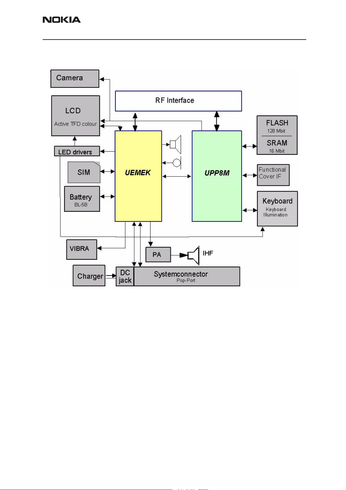
Baseband
The RH-37 product is a DCT4.5 Expression segment phone. There are two variants: An
EGSM900/GSM1800/GSM1900 phone and a US variant, RH 49, with GSM850/1800/
1900.
The HW has the following features:
• GPRS and HSCSD with EDGE in up to (2RX + 2TX) (MCS5), without EDGE also in
(3RX + 1TX) (MCS6)
• DCT4 with AMR and 16 MIDI tones
• 128/16 Mbit Combo memory
• Amazon Active display with 64k colours
•Battery BL-5B
• Illuminated XPress on grips
• PopPortTM interface
• 5-way navigation key with select
• FCI rear side (C-cover)
•VGA Camera
•Vibra
•IHF
TM
The RH-37 BB is based on the DCT4/4.5 engine and is compatible to the PopPort
accessories. The DCT4/4.5 engine consists basically of two ASICs. The UEMEK (Universal
Energy Management IC including voltage regulators, charge control and audio circuits,
audio IFH amplifier from DCT4.5) and the UPP (Universal Phone Processor including MCU,
DSP and RAM from DCT4).
Page 10 ©Nokia Corporation Issue 1 07/04
RH-37
Nokia Customer Care System Module
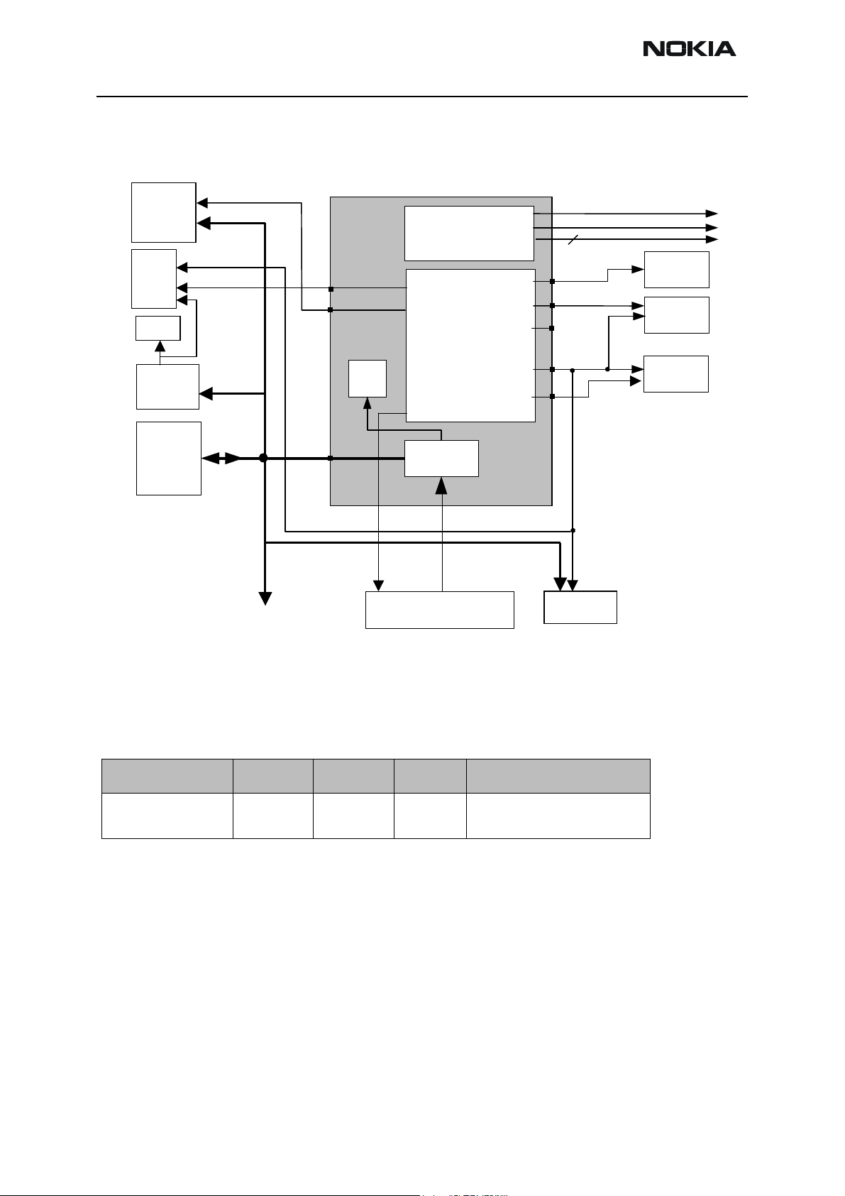
Block diagram
Figure 1: Baseband block diagram
UEMEK supplies both baseband and RF with power via built in voltage regulators, which
are connected to the battery. The RF parts use mainly 2.78 V and the baseband parts 1.8V
I/O voltage. The UPP core is supplied with programmable core voltage of 1.0V, 1.3V or
1.5V. UEMEK includes 7 linear LDO (Low Drop-Out) regulators for baseband and 7 regulators for RF. It also includes 4 current sources for biasing purposes and internal usage. The
UEMEK is furthermore supplying the SIM interface with a programmable voltage of 1.8V
or 3V.
Note: 5V SIM cards are no longer supported by DCT-4 generation Baseband.
UPP operates from a 26 MHz clock coming from the RF ASIC Helgo. The clock signal is
divided by two down to the nominal system clock frequency of 13 MHz. The DSP and
MCU contain PLLs, which can multiply the system clock to a higher frequency.
A real time clock function is integrated into the UEMEK, which utilizes the same 32kHz
clock supply as the sleep clock.
The communication between UEMEK and UPP is implemented using two bi-directional
serial busses, CBUS and DBUS. The CBUS is controlled by the MCU and operates at a
Issue 1 07/04 ©Nokia Corporation Page 11

RH-37
System Module Nokia Customer Care
speed of 1 MHz. The DBUS is controlled by the MCU and operates at a speed of 13 MHz.
Both processors are located in the UPP.
The UEMEK ASIC handles the analog interface between the Baseband and the RF section.
UEMEK provides A/D and D/A conversion of the in-phase and quadrature receive and
transmit signal paths and also A/D and D/A conversions of received and transmitted
audio signals to and from the user interface. The UEMEK supplies the analog TXC and
AFC signals to the RF section according to UPP signal control. There are also separate
signals for PDM coded audio. Digital speech processing is handled by the DSP inside UPP
ASIC.
UEMEK is a dual voltage circuit, the digital parts are running from the baseband supply
1.8V and the analog parts are running from the analog supply 2.78V. Also VBAT is
directly used (Vibra, LED-driver, Camera Regulator, FCI).
The Baseband supports both internal and external microphone inputs and speaker outputs. Keypad tones, DTMF, and other audio tones are generated and encoded by the UPP
and transmitted to the UEMEK for decoding. An external vibra alert control signals are
generated by the UEMEK with separate PWM outputs.
EMC shielding is implemented using a soldered shielding, RF cans and PWB grounding.
Page 12 ©Nokia Corporation Issue 1 07/04
RH-37
Nokia Customer Care System Module
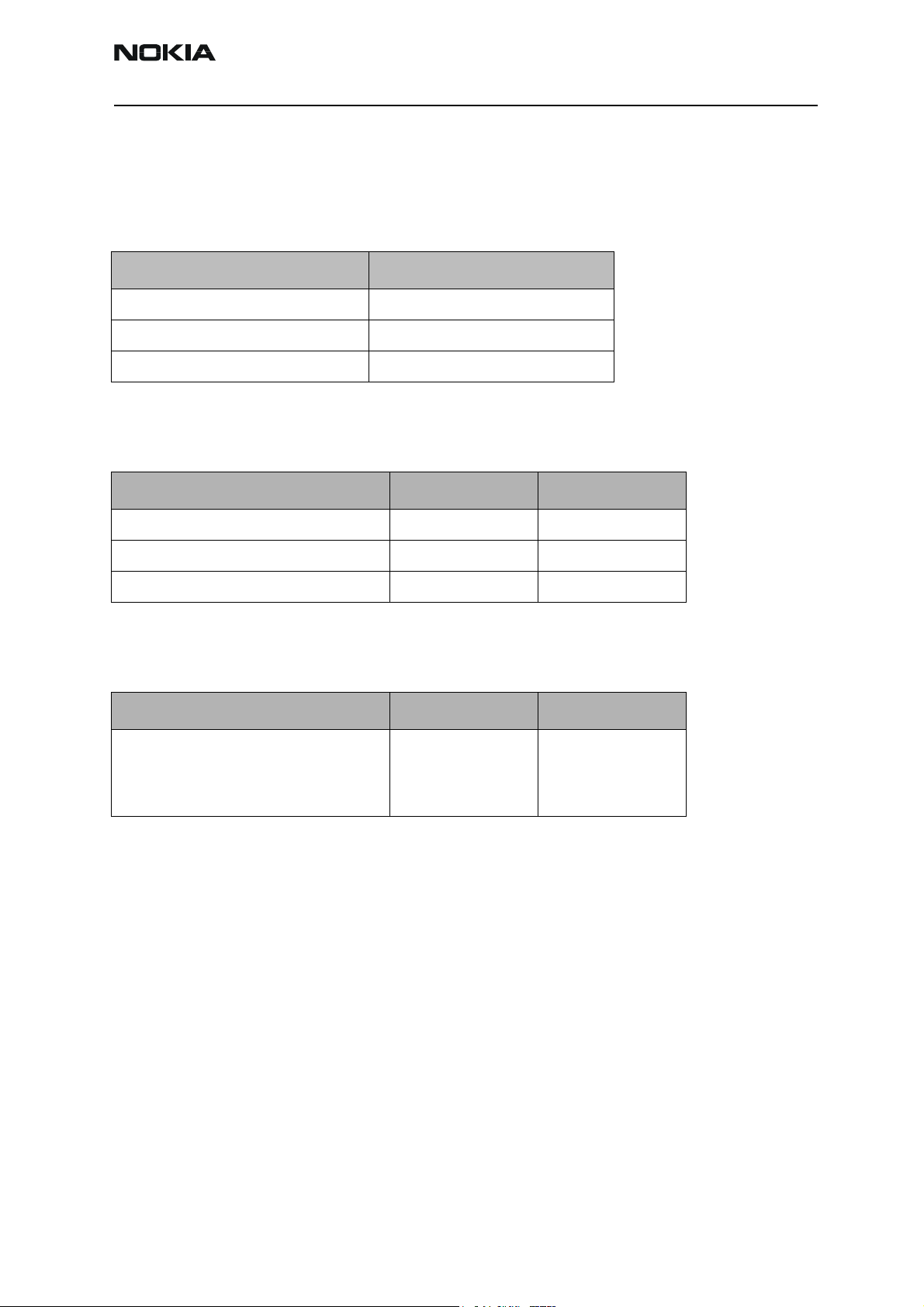
Environmental Specifications
Absolute maximum ratings
Table 1: Absolute maximum ratings
Signal Note
Battery Voltage (Idle) -0.3…5.5V
Battery Voltage (Call) Max 4.8V
Charger Input Voltage -0.3V …16V
Temperature conditions
Table 2: Temperature conditions
Condition Min Max
Normal operating temperature -10°C+55°C
Reduced functionality -25°C+75°C
Storage -40°C+85°C
Humidity and water resistance
Table 3: Humidity conditions
Condition Min Max
Relative Humidity 5%
C
The module is not protected against water.
95%
Issue 1 07/04 ©Nokia Corporation Page 13
RH-37
System Module Nokia Customer Care
Frequencies in baseband
Table 4: Frequencies in baseband
Frequency Context UPP UEMEK Flash SIM Comment
100 kHz FCI X X
32 kHz SleepClk X
1 MHz CBUS X X
Up to 1 MHz RFConvClk X X Estimation
6,5 MHz Display IF X
3,25 MHz SIMIF X X Min
13 MHz DBUS, RFBUClik X X
26 MHz RF Clk X
52 MHz Memory Clock X X
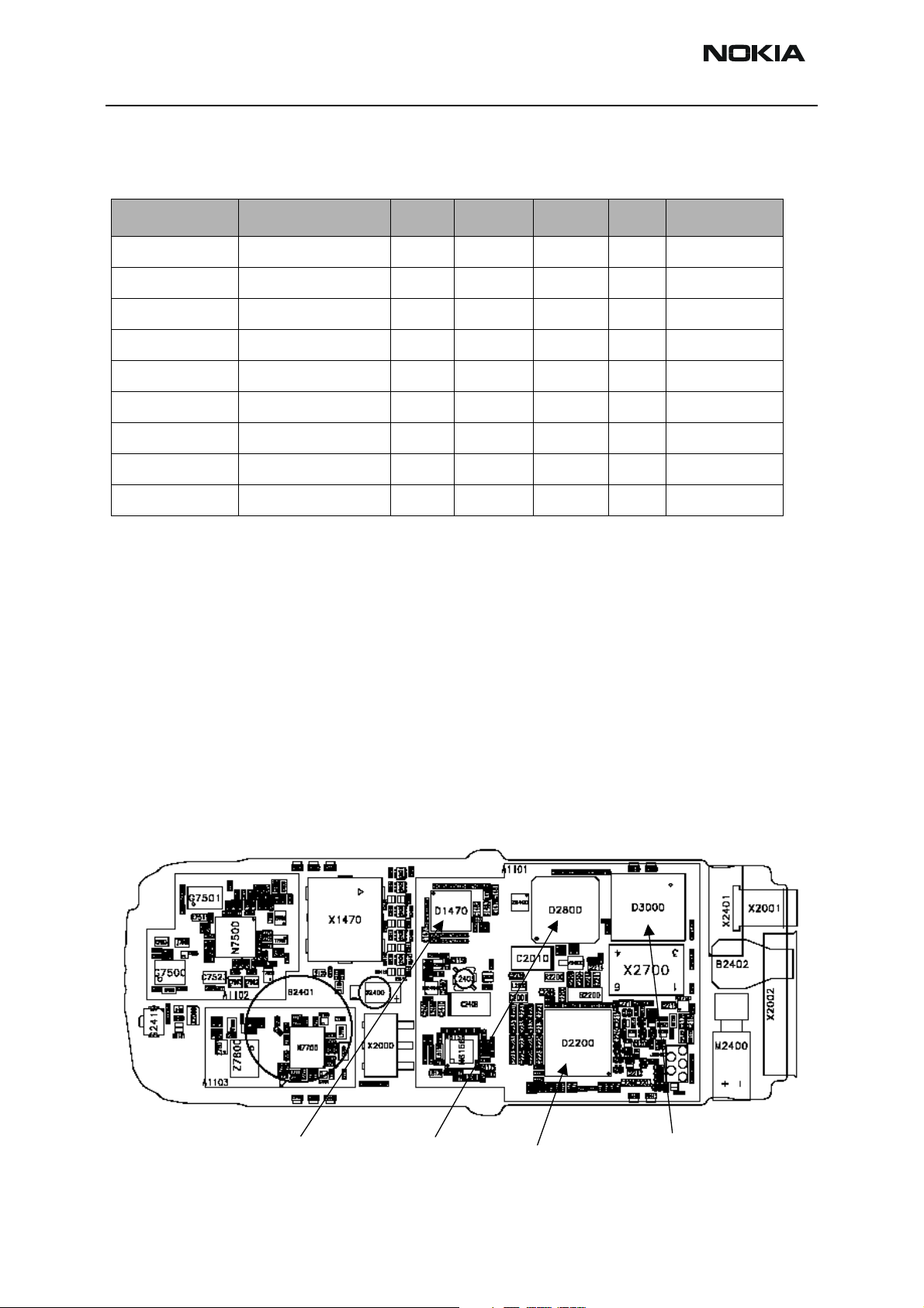
PWB
Characteristics of the PWB
• Single PWB
• 8 layer board
• Double side assembled
Key components
Figure 2: Key components
D1470 HW Accelerator
D2800 UPP
D2200 UEMEK
D3000 Combo
Page 14 ©Nokia Corporation Issue 1 07/04
RH-37
Nokia Customer Care System Module
Table 5: Key components
Position Component Name Code
D1470 HW Accelerator 4377033
D2800 UPP8M v 3.5 4371105
D2200 UEMEKv2.0 4376371
D3000 Combo Memory (128M NOR + 16M UTRAM) 4347043
Issue 1 07/04 ©Nokia Corporation Page 15

RH-37
System Module Nokia Customer Care
Technical Specifications
Baseband core
UPP
Main characteristics of the used UPP are:
• DSP, LEAD3 16 bit DSP core 32 bit IF max. 200 MHz
• MCU based on ARM7 RISC MCU core max 50 MHz
• Internal 8 Mbit SRAM (PDRAM)
• General purpose UARTS
• SIM card interface
UEMEK
• Accessory interface (ACI)
• Interface control for Keypad, LCD, Audio and UEM control
• Handling of BB-RF Interface
Main characteristics of the used UEMEK are:
• ACI support
• Audio codec
• 11 Channel A/D converter
• Auxiliary A/D converter
• 32 KHz crystal oscillator
• SIM interface and drivers
• Security logic
• Storage of IMEI code
• Buzzer and vibra motor drivers
•PWM
• 2 LED drivers, keyboard and display backlight drivers
Page 16 ©Nokia Corporation Issue 1 07/04
RH-37
e
Nokia Customer Care System Module
• Voltage reference for analogue blocks
• Charging function
• Baseband regulators
• RF regulators
• RF interface converters
External SRAM and Flash
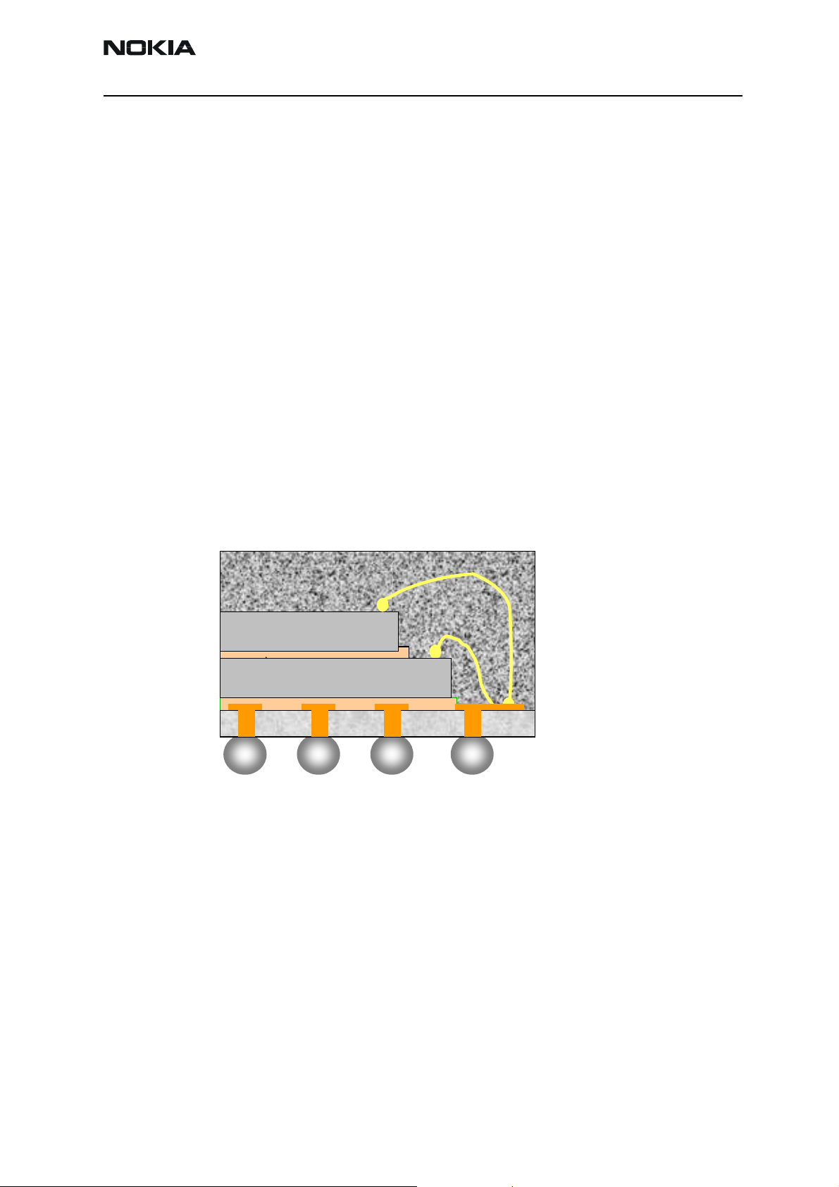
The Combo-Memory is a multi chip package memory which combines 128 Mbit (8Mx16)
muxed burst multibank flash and 16 Mbit muxed CMOS PSRAM (Pseudo SRAM: DRAM
with SRAM interface).
The combo is supplied by single 1,8 V for read, write and erase operations. For accelerated flash programming, Vpp = 9.0 V has to be applied to VPP input of the combo device.
The combo memory is housed in a 44-ball FBGA.
Energy management
The energy management of RH-37 is based on BB 4.0 architecture. A so-called semi fixed
battery (BL-5B) supplies power primarily to UEMEK ASIC and the RF PA. The UEMEK
includes several regulators to supply RF and Baseband. It provides energy management
including power up/down procedure.
2nd
1st Chip
Figure 3: Combo memory
PI
Modes of operation
The baseband engine has six different functional modes: Since the UEMEK controls the
regulated power distribution; each of these states affects the general functionality of the
phone.
1 No supply
Issue 1 07/04 ©Nokia Corporation Page 17

RH-37
System Module Nokia Customer Care
2 Backup
3Acting Dead
4Active
5 Sleep
6 Charging
No Supply
In NO_SUPPLY mode, the phone has no supply voltage. This mode is due to the disconnection of the main battery and backup battery or low battery voltage level in both of
the batteries.
The phone is exiting from NO_SUPPLY mode when sufficient battery voltage level is
detected. The battery voltage can rise either by connecting a new battery with VBAT >
V
or by connecting charger and charging the battery above V
MSTR+
MSTR+
.
Backup
In BACKUP mode the backup battery has sufficient charge but the main battery can be
disconnected or empty (VBAT < V
The VRTC regulator is disabled in BACKUP mode. VRTC output is supplied without regulation from the backup battery (VBACK). All the other regulators are disabled.
BACKUP mode is not used in RH-37 since the product has no backup battery.
Acting Dead
If the phone is off when the charger is connected, the phone is powered on but enters a
state called ”Acting Dead”. To the user, the phone acts as if it was switched off. A battery-charging alert is given and/or a battery charging indication on the display is shown
to acknowledge the user that the battery is being charged.
Active
In the Active mode the phone is in normal operation, scanning for channels, listening to
a base station, transmitting and processing information. There are several sub-states in
the active mode depending on if the phone is in burst reception, burst transmission, if
DSP is working etc.
and VBACK > VBU
MSTR
COFF
).
In Active mode the RF regulators are controlled by SW writing into UEMEK´s registers
wanted settings: VR1A can be enabled or disabled. VR2 can be enabled or disabled and
its output voltage can be programmed to be 2.78V or 3.3V. VR4-VR7 can be enabled, disabled, or forced into the low quiescent current mode. VR3 is always enabled in Active
mode.
Page 18 ©Nokia Corporation Issue 1 07/04

RH-37
Nokia Customer Care System Module
Sleep Mode
Sleep mode is entered when both MCU and DSP are in stand–by mode. Both processors
control the sleep mode. When SLEEPX signal (low) is detected UEMEK enters SLEEP
mode. VCORE, VIO and VFLASH1 regulators are put into low quiescent current mode. All
the RF regulators are off in SLEEP. When SLEEPX=1 detected UEMEK enters ACTIVE mode
and all functions are activated.
The sleep mode is exited either by the expiration of a sleep clock counter in the UEMEK
or by some external interrupt, generated by a charger connection, key press, headset
connection etc.
In the sleep mode, VCTCXO is shut down and 32 kHz sleep clock oscillator is used as reference clock for the Baseband.
Charging
In RH-37, the battery type/size is indicated by a BSI-resistor. The resistor value corresponds to a specific battery capacity. Also BTEMP, NTC resistor, is located on an engine
board.
The battery voltage, temperature, size and current are measured by the UEMEK controlled by the charging software running in the UPP.
The charging control circuitry (CHACON) inside the UEMEK controls the charging current
delivered from the charger to the battery. The battery voltage rise is limited by turning
the UEMEK switch off when the battery voltage has reached 4.2 V. Charging current is
monitored by measuring the voltage drop across a 220 mΩ resistor.
Power distribution
Under normal conditions, the battery powers the baseband module. Individual regulators
located within the UEMEK regulate the battery voltage VBAT. These regulators supply the
different parts of the phone. 7 regulators are dedicated to the RF module and 7 to the
baseband module.
The VSIM regulator is able to deliver both 1,8V and 3,0 V DC and thus supporting two
different SIM technologies.
The regulator VCORE is likewise adjustable by the MCU. VCORE supplies the core logic of
the UPP.
The system connector provides a voltage to supply accessories.
The white LEDs need a higher voltage supply than the battery can supply and are fed by a
separate external voltage regulator.
VBAT is directly distributed to the RF power amplifier, FCI and external baseband regulators.
Issue 1 07/04 ©Nokia Corporation Page 19
RH-37
y
System Module Nokia Customer Care
Figure 4: Power Distribution Diagram
CAMERA
LCD
LEDs
White LED
Driver
Battery
Baseband
UEME
RF Regulators
VFLASH1
VAUX3
VLED+
Baseband
RTC
VBAT
PA Supply
Regulators
VAUX2
CHACON
Vout
System Connector
VR1A
VR1B
VR2-7
VSIM
VCORE
VANA
VIO
VFLASH1
VBAT
To RF Part s
6
FCI
SIM
UPP
Combo
Memor
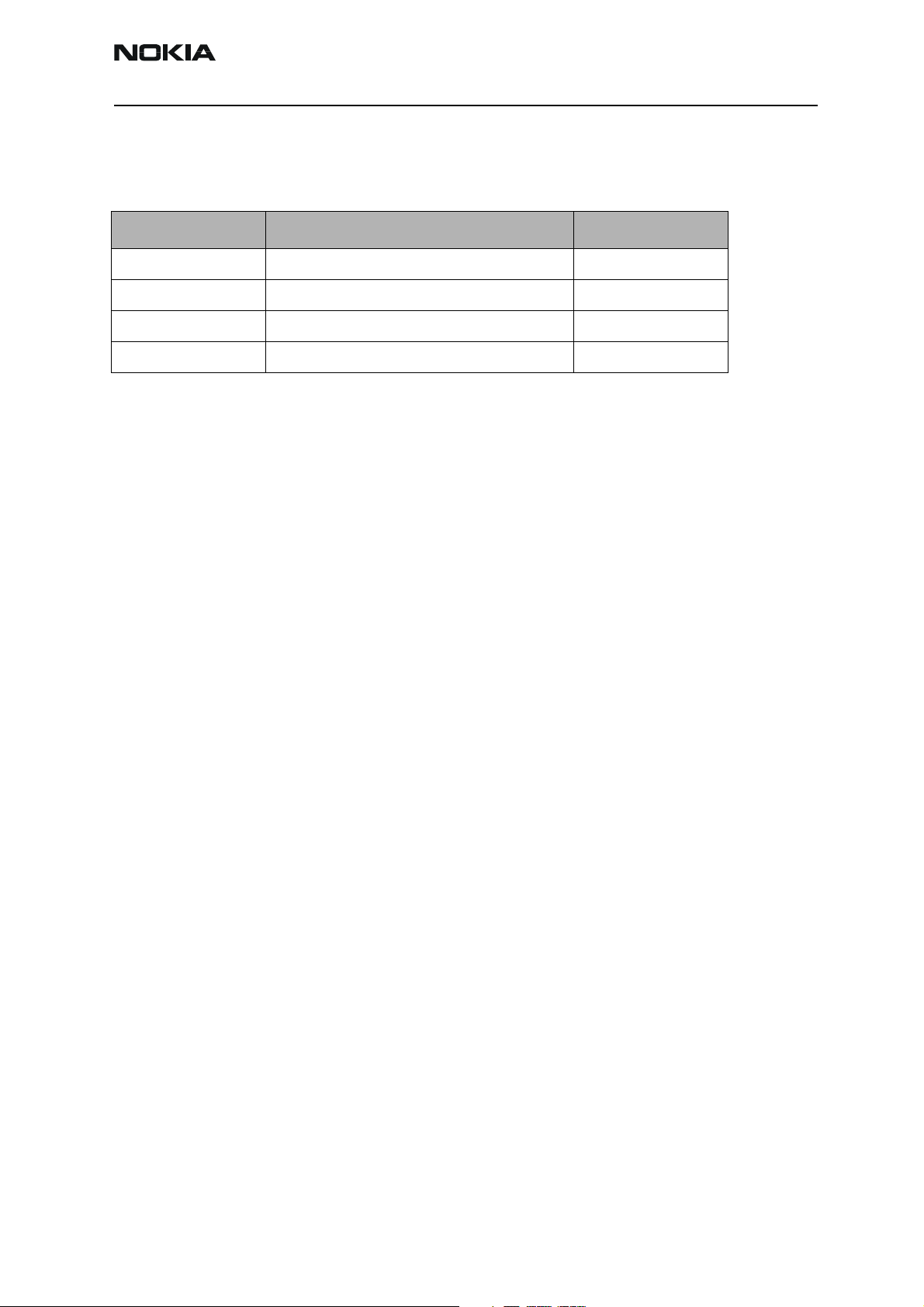
DC characteristics
Supply voltage ranges
Table 6: Battery voltage ranges
Signal Min Nom Max Note
VBAT 3.1V 3.7V 4.2V 3.2V SW cut off
2.95V HW power off
Page 20 ©Nokia Corporation Issue 1 07/04
RH-37
Nokia Customer Care System Module
Baseband regulators
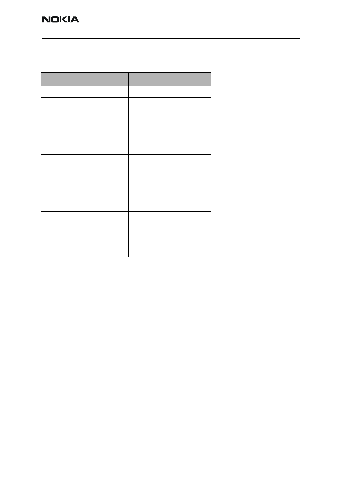
Table 7: Regulator specification
Regulator Load current (mA) Limit (V) Min/Max (Typ)
VCORE 200 1.476 / 1.65 (1.57)
VIO 150 1.72 / 1.88 (1.8)
VSIM1 25 1.745 / 1.855 (1.8)
VANA 80 2.70 / 2.86 (2.78)
VFLASH1 70 2.70 / 2.86 (2.78)
VAUX2 70 2.70 / 2.86 (2.78)
VAUX3 10 2.70 / 2.86 (2.78)
VR2 100 2.70 / 2.86 (2.78)
VR3 20 2.70 / 2.86 (2.78)
VR4 50 2.70 / 2.86 (2.78)
VR5 50 2.70 / 2.86 (2.78)
VR6 50 2.70 / 2.86 (2.78)
VR7 45 2.70 / 2.86 (2.78)
VR1A 5* 4.6 / 4.9 (4.75)
VR1B 5* 4.6 / 4.9 (4.75)
* When both enabled. Load current is 10 mA if other is disabled.
Note: This list shows the band regulators only. Please see other descriptions in the Glossary of Terms
and in the dedicated sections.
Issue 1 07/04 ©Nokia Corporation Page 21
 Loading...