

Page 1

PAMS Technical Documentation
TFE–1 model C
TROUBLESHOOTING
INSTRUCTIONS
Original 11/97
Page 2
TFE–1 model C
PAMS
Troubleshooting Instructions
AMENDMENT RECORD SHEET
Amendment
Number
Date Inserted By Comments
Technical Documentation
Page 2
Original 11/97
Page 3

PAMS
TFE–1 model C
Technical Documentation
Troubleshooting Instructions
TFE–1 model C TROUBLESHOOTING INSTRUCTIONS
Contents
Introduction Page 4. . . . . . . . . . . . . . . . . . . . . . . . . . . . . . . . . . . . . . . . . . . .
General Page 4. . . . . . . . . . . . . . . . . . . . . . . . . . . . . . . . . . . . . . . . . . . . .
Baseband Troubleshooting Page 5. . . . . . . . . . . . . . . . . . . . . . . . . . . . . . .
1. Terminal is Totally Dead Page 6. . . . . . . . . . . . . . . . . . . . . . . . . . . . .
2. Flash Programming Doesn‘t Work Page 7. . . . . . . . . . . . . . . . . . . .
3. Power Doesn‘t Stay On or The Phone is Jammed Page 10. . . . . .
Function of the 32 kHz Clock Oscillator in Test Circumstances Page 10
4. LED Indication or Handset‘s display Information: Contact Service Page 12
5. The Terminal Doesn‘t Register to The Network (no serv)
or Doesn‘t Make a Call Page 14
The States of The DSP after Power On Page 14. . . . . . . . . . . . . . .
6. SIM Card is Out of Order (Insert SIM Card or Card Rejected) Page 16
7. Audio Fault Page 18. . . . . . . . . . . . . . . . . . . . . . . . . . . . . . . . . . . . . . . .
8. Line Adapter troubleshooting:
Terminal works with handset, but not with device Page 21
9. Immobilizer troubleshooting (in TFE–1 model C) Page 22. . . . . . . .
Switch mode power supply problems Page 23. . . . . . . . . . . . . . . . . . . .
Original 11/97
Page 3
Page 4

TFE–1 model C
PAMS
Troubleshooting Instructions
Introduction
General
The purpose is to define fault block of the module and then find out the broken
component. The trouble shooting diagram has been planned so that the fault,
whatever it is, can be found by as simple measurements as possible.
The flow diagrams give you the overview of the blocks. The purpose is that you
proceed through the flow diagram so that, if your answer is YES for the asked
question, go straight to the next level, but if your answer is NO, you have to go
the subbranch.
Required servicing equipment:
– PC for Service Software
– Power supply (2.0 A)
– Digital multimeter
– Oscilloscope
Technical Documentation
– Spectrum analyzer
– Signal generator
– RF cables
– Modular cable
– RS232/MBUS adapter
– RF measuring chassis
– Termination
The Troubleshooting for TFE–1 model C consists of a series of checks accord-
ing to the following flow diagrams.
Page 4
Original 11/97
Page 5

PAMS
TFE–1 model C
Technical Documentation
Baseband Troubleshooting
The following hints should facility finding the cause of the problem when the circuitry seems to be faulty. This troubleshooting instruction is divided following
section.
1. Terminal is totally dead
2. Flash programming doesn‘t work
3. Power doesn‘t stay on or the terminal is jammed
4. Display information: Contact Service
5. Terminal doesn‘t register to the network or terminal doesn‘t make a call.
6. Plug in SIM card is out of order (insert SIM card or card rejected).
7. Audio fault.
8. Line Adapter trouble shooting
9. Immobilizer troubleshooting
The first thing to do is carry out a through visual check of the module. Ensure in
particular that:
a) there are not any mechanical damages
b) soldered joints are OK
Troubleshooting Instructions
Original 11/97
Page 5
Page 6
TFE–1 model C
PAMS
Troubleshooting Instructions
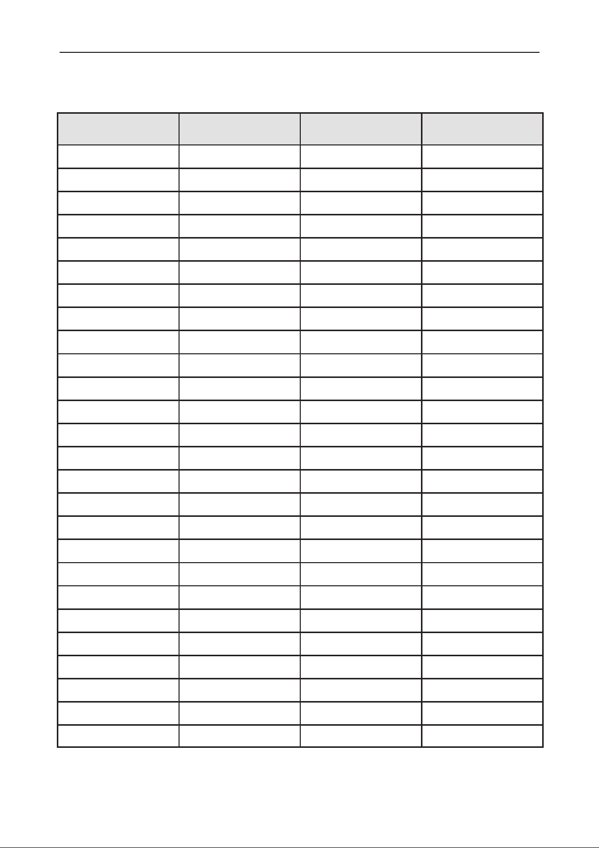
1. Terminal is Totally Dead
Troubleshooting diagram for this fault is represented in following figure. Check
at first that the battery back is OK and it is not empty. This kind of fault has
been limited around the system connector (X103) and the PSCLD (N301).
If the phone is totally dead,
check that the fuse is OK
Voltage level at
PSCLD (N300)
pin 25 is same
as VBA T
YES
Measure voltage
level at PSCLD
(N300) pin 40
NO
Technical Documentation
PSCLD N300
pins 5,21,37...
voltage level is
same as VBAT
NO
Check coils L302,
L303 and the sol–
dered joints of the
connector X120,
fuse F100
YES
Rise up PSCLD
pin 25.
If the DC voltage
is still missing
change N300
NO
Check soldered
joints of V302,
V303, V304, and
around components
The voltage level at
pin 40 (N300) is zero
Rise up PSCLD pin 25.
NO
If the DC voltage is still
missing, change N300
Check that capacitors C311,
C312, C315, C317 and C318
are soldered. Check also soldered joints of N300. If these
things are correct, change
N300
YES
Page 6
Original 11/97
Page 7

PAMS
TFE–1 model C
Technical Documentation
2. Flash Programming Doesn‘t Work
The block diagram for the flash programming is shown in figure 12. The flash
loading is handled via these components. Thus a fault in other components
(DSP, RFI) can not prevent the flash loading.
In error cases, the flash prommer can give some information about a fault.
The fault information messages could be:
– MCU doesn‘t boot
– MCU flash Vpp error
– Serial data line failure
– Serial clock line failure
– External RAM fault
– Algorithm file or alias ID don‘t find
In cases that the the flash programming doesn‘t succeed, there is a possibility
to test the interface between the ASIC and the MCU.
This test is useful to do, when the fault information is: MCU doesn‘t boot or Serial clock line failure.
The test procedure is following:
Troubleshooting Instructions
1. Connect a short circuit wire between the test points J400 and J401.
2. Switch power on.
3. If the reset line of the MCU rises up, the interface is OK. Otherwise the reset
line stays low.
One must be noticed that this test can be found only short circuits, not open
pins. This test indicate also that 32 kHz clock is running because of the test logic is made by using 32 kHz clock oscillator.
Original 11/97
Page 7
Page 8
TFE–1 model C
PAMS
Troubleshooting Instructions
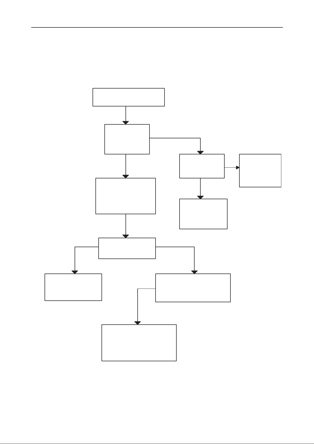
Flash programming doesn‘t work
Output voltages of PSCLD (N300)
are 3.16 V ( VL, VA, VSL )
Master Reset (Purx), PSCLD pin 26
is ”1” ( 3.16 V )
Master clock input, ASIC (D400)
pin 22 is 13 MHz, 1 Vpp, sine
wave with 1 V DC level
Clock signal at the input of MCU, pin 51
is 13 MHz square wave.
YES
YES
YES
Technical Documentation
NO
NO
NO
NO
Check the soldered joints of
N300. If OK, change N300
Rise up pin 26. If the logic
level is still ”0”, check soldered joints of N300. If OK,
change N300.
Check components R400 and C403.
If they are OK, check the VCXO
block. One must remember that the
control signal for the VCXO is taken
from the baseband (see figure 6 )
Check resistor R437. Check the
soldered joints of ASIC. If OK,
change ASIC
YES
NO
MCU Reset input, pin 48 is ”1”
Rise up MCU pin 48. If the logic
level is still ”0”, check the soldered joints of the ASIC. If OK,
YES
change ASIC.
Check that the following lines are correct.
1. Vpp line from X120 pin 7 to FLASH (D430) pin 11
Normal fault information: MCU FLASH Vpp error
2. MBUSRX line from X120 pin 1 to MCU (D420) pin 2
Normal fault information: Serial data line failure
3. MBUSTX line from X120 pin 2 to MCU (D420) pin 1
Normal fault information: MCU doesn‘t boot
4. MBUSCLK line from X120 pin 3 to MCU (D420) pin 3.
Check also R436.
Normal fault information: Serial clock line failure
5. WDDIS line from X120 pin 4 to PSCLD (N300) pin 22
6. GND (X120 pin 15) is connected to ground
Page 8
Original 11/97
Page 9

PAMS
TFE–1 model C
Technical Documentation
1. Connect a short circuit wire between the test points
J400 and J401
2. Switch power on and measure the state of the
MCU Reset line (pin 48)
If the Reset line rises up to ”1” state there are not short circuits
In cases that fault information is
a) MCU doesn‘t boot
b) Clock line serial failure
the ASIC self test function can be used
Reset is ”1”
Check that there are not open pins
in components: D420, D400, D430,
D440
Troubleshooting Instructions
Reset is ”0”
There is a short circuit between
the pins.
Check circuits: D420, D400
D430, D440
In case that fault information is:
External RAM fault
Check the pins of SRAM (D440)
Check also the control lines of SRAM:
WrX, RdX from MCU;
RAMCS from ASIC
(see figure 12)
In case that fault information is:
Algorithm file or alias ID don‘t
find, ID is unkwon etc.
Check pins of the FLASH (D430)
Check also the control lines of FLASH:
WrX, RdX from MCU
CSelX, PwrDown from ASIC
(see figure 12)
Original 11/97
Page 9
Page 10

TFE–1 model C
PAMS
Troubleshooting Instructions
Technical Documentation
3. Power Doesn‘t Stay On or The Phone is Jammed
If a fault has come after the flash programming, there are most probably open
pins in IC‘s.
The soldered joints of IC’s: D420 (MCU), D400 (ASIC), N300(PSCLD), D430
(FLASH), D440 (SRAM) is useful to check at first.
Normally, the power switch off after 30 seconds, if the watchdog of the PSCLD
can not be served by software. The power off function can be prevented by
connecting a short circuit wire from the PSCLD pin 22 (WDDIS) to the ground.
If the power switches off after 1..2 seconds, the pins of PSCLD and the
PSCLD‘s auxiliary components must be checked.
If the phone is jammed, and no other reason has been found, the function of 32
kHz clock oscillator must be checked. This can be done by setting the phone to
the ASIC self test mode.
1. Connect a short circuit wire between the test points J400 and J401.
2. Make a short circuit between the ASIC pins 78 and 79.
3. Switch power on.
4. Measure the signal by oscilloscope at pins 78, 79 (ASIC).
Function of the 32 kHz Clock Oscillator in Test Circumstances
PSCLD pin 26, PurX
(Master Reset)
ASIC pin 78 (MCUIRQ1X) and
ASIC pin 79 (MCUIRQ0X)
30.5 us
1 V
Page 10
Original 11/97
Page 11

PAMS
TFE–1 model C
Technical Documentation
Connect a short circuit wire from PSCLDs
pin 22 to the ground. This make sure that
power stays on during the measurements
Power doesn‘t stay on or
the phone is jammed
(In case that fault has come after the flash programming).
Output voltages of PSCLD (N300)
are 3.16 V (VL, VA, VSL).
YES
Master Reset, PSCLD pin 26,
is ”1” (3.16 V)
YES
Troubleshooting Instructions
ATTENTION !
Do not forget to check needed PCB wires between the
circuits.
NO
NO
Check the soldered joints
of N300. If OK, change
N300.
Rise up pin 26. If the logic level is still ”0”,
check soldered
joints of N300. If OK,
change N300.
NO
Check resistor
R437.
Check that Master
Reset input pin,
ASIC pin 120 is ”1”.
If it is ”1” check
soldered joints of
ASIC. If OK,
change ASIC.
Master clock input, ASIC (D400) pin 22,
13 MHz about 1 Vpp sine wave signal
with 1 V DC level (see figure X)
YES
MCU (D420) clock signal input, pin 51,
6.5 MHz square wave signal (see figure
X).
YES
MCU reset input, pin 48 is ”1”
YES
Check that there are not open pins
in components D420 (MCU), D400
(ASIC), D430 (FLASH), D440
(SRAM)
OK
Check the function of the 32 kHz oscillator
(see page 40)
NO
NO
Check components R400
and C403. If they are OK,
check the VCXO block.
One must remember, that
the control signal for the
VCXO power supply is taken from baseband (see figure X).
Rise up pin 48. If the logic
level is still ”0”, check the
soldered joints of the ASIC.
If OK, change ASIC.
Original 11/97
Page 11
Page 12

TFE–1 model C
PAMS
Troubleshooting Instructions
Technical Documentation
4. LED Indication or Handset‘s display Information: Contact
Service
If LED combination suggests ”Contact Service” in TFE–1 Model C, it may also
be because immobilizer has gone off. Check the state of immobilizer with handset. If it shows ”Install terminal” or ”Terminal moved”, contact your local operator for assistance.
”Contact Service” means that MCU is able to run and the watchdog of the
PSCLD (N300) can be served. Thus PCLocals functions can be used and some
information about the fault is possible to get.
In principle, the fault for contact service information can be found around ASIC
(D400), DSP (D360), RFI (N450), EEPROM (D445) or AUDIO CODEC (N130).
Page 12
Original 11/97
Page 13

PAMS
TFE–1 model C
Technical Documentation
NO
Check the soldered joints
of ASIC (D400). If OK,
change D400
Led or Handset‘s information: Insert SIM
card of card rejected
DSP (D360) pin 66
(or testpoint J361)
NO
39 MHz square wave
YES
DSP pin 69 (XRES)
is ”1”.
YES
DSP pin 20 (XF) or testpoint J360
250 ms
Power On
Software download to
external RAMs
YES
XF stays ”1” after
download
Troubleshooting Instructions
DSP pin 68: 13 MHz
square wave
YES
Check the soldered joints
of DSP (D360). If OK,
change D360
Check R361 and soldered
joints of ASIC (D400). If
OK Change D400
Download is failed. Check
NO
soldered joints of ASIC
(D400) and DSP (D360)
NO
Check soldered joints of DSP (D360) and
external RAMs D371, D372
RFI (N450) pin 51 (SYSRESX)
is ”1”.
YES
RFI (N450) pin 45: 13 MHz
NO
square wave
YES
Check soldered joints of
RFI (N450), DSP
(D360), ASIC (D400)
Check soldered joints of EEPROM (D445)
and connections to the MCU (D420).
Check soldered joints of AUDIO CODEC
(N130) and connections to the ASIC (D400).
Check the soldered joints
NO
of ASIC (D400). If OK,
change D400
Check the soldered joints
of ASIC (D400). If OK,
change D400
Original 11/97
Page 13
Page 14

TFE–1 model C
PAMS
Troubleshooting Instructions
Technical Documentation
5. The Terminal Doesn‘t Register to The Network (no serv)
or Doesn‘t Make a Call
If the terminal doesn‘t register to the network or the terminal doesn‘t make a
call, the reason for this could be either the baseband or the RF part. The terminal can be set to wanted mode by PCLocals software and try to find reason for
fault.
The control lines for RF are supplied both the ASIC (D400) and the RFI (N450).
The ASIC handles digital control lines (between ”0” = 0 V and ”1” = 3.16 V) and
the RFI handles analog control lines and proper input and output signals.
The DSP uses its external flag outpin (XF pin 20) as an indicator of its operation state. During power up, DSP signals all completed functions by changing
the state of the XF pin (see figure 38).
The States of The DSP after Power On
XF (pin 20) is ”1” after power on
1
DSP pin 20 (XF)
2 3 4 5
2
DSP code download starts
DSP code download starts
DSP has performed self tests and
3
1
6 7
initalization succesfully
DSP has received SEARCH_LIST
4
command from MCU
( DSP starts channel search)
DSP starts PSW search
5
( Channel has been found)
( Rx and AGC are OK )
PSW has been found
6
( the synthesizer works OK)
DSP has received synchroniza–
7
tion.
( AFC works OK)
Page 14
Original 11/97
Page 15

PAMS
TFE–1 model C
Technical Documentation
Troubleshooting Instructions
5. The Terminal doesn’t register to the network (No Serv) or
doesn’t make a call (cont.)
Phone doesn‘t register
to the network or phone
doesn‘t make a call
Check transistor V300. Check RF regu–
NO
lator N601. One must remember, that
control signal for RF regulator N601 (pins
12 and 16) is taken from ASIC (D400) pin
130 and routed to the RF via PSCLD
(N300) pins 17, 13.
Check the soldered joints
of ASIC (D400) and the
connections to the RF part
NO
Check components C457
and C458. If OK, Change
RFI (N450)
ASIC pin 33 (RxPwr) is ”1” during the receive slot
ASIC pin 34 (SynthPwr) is ”1” during the receive slot
ASIC pin 35 (SEna1X) is ”0” during the receive slot
ASIC pin 39 (SCLK) is ”1” during the receive slot
ASIC pin 38 (SDATA) is ”1” during the receive slot
RFI (N450) pins 9,10,11
DC level 4.5 V
YES
RFI (N450) pin 3 (REFOUT)
DC level 2.5 V
YES
YES
RFI pin 16 (TXCOUT) is ”1” during the receive slot
RFI pin 24 (PDATA0) is ”1” during the receive slot
RFI pin 24 (PDATA0) is ”1” during the receive slot
RFI pin 54 (RXINN): DC level 1.6 V during the receive slot
RFI pin 55 (RXINP): DC level 1.6 V during the receive slot
RFI pin 64 (AFC) : 1 V < DC level < 3 V
YES
Use PCLocals functions to turn transmitter on
ASIC pin 31 (TXP) is ”1” during the transmit slot
ASIC pin 32 (TXPWR) is ”1” during the transmit slot
YES
4.6 ms
YES
RFI pin 1 (TXQN)
RFI pin 2 (TXQP)
RFI pin 12 (TXIN)
2.6 V
1.1 V
RFI pin 13 (TXIP)
NO
Check the soldered joints
of RFI (N450) and the connections to the RF part
Check the soldered joints
NO
of ASIC(D400) and the
connections to the RF part
Check the soldered joints
NO
of RFI (N450) and the connections to the RF part
CHECK RF P ART
Original 11/97
0.6 ms
Page 15
Page 16

TFE–1 model C
PAMS
Troubleshooting Instructions
Technical Documentation
6.SIM Card is Out of Order (Insert SIM Card or Card Rejected)
The hardware of the SIM interface from the ASIC (D400) to the SIM connector
(X300) can be tested without SIM card. When the power is switched on, all the
used lines (VSIM, RST, CLK, DATA) rises up to ”1” (5 V) four times. Thus the
fault can be found without the SIM card in most cases.
Display information:
Insert SIM card or
card rejected
YES
ASIC (D400) pin 25
(CARDDETX):
DC level < 2 V
YES
PSCLD (N300) pin15 (SIMENA):
pulses up to ”1” (3 V), when the
power is switched on
NO
NO
Check N350 pin 5, V404,
R407, R408 and R409
Check connection to the ASIC; pin 30
Check also soldered joints of
ASIC (D400) and PSCLD (N300)
YES
PSCLD (N300) pin 10 (SIM_I/O_CTRL):
pulses up to ”1” (3 V), when the power is
switched on
YES
SIM CONNECTOR (X300) pin C1 (VCC):
pulses up to ”1” (5 V), when the power is
switched on
YES
SIM CONNECTOR (X300) pin C2 (RST):
pulses up to ”1” (5 V), when the power is
switched on
YES
PSCLD (N300) pin 9 (SIMRST_A):
pulses up to ”1” (3 V), when the
power is switched on
Check connection to the ASIC;
pin 28 (SIMRESETX).
Check also soldered joints of
ASIC (D400) and PSCLD (N300)
Check connection to the ASIC;
NO
pin 26.
Check also soldered joints of
ASIC (D400) and PSCLD (N300
NO
Check connection to the PSCLD
(N300) pin 41 and the soldered
joints of PSCLD (N300)
NO
PSCLD (N300) pin 2 (SIMRST_S):
pulses up to ”1” (5 V), when the
power is switched on
NO
NO
YES
Change N300
YES
Check R331
Page 16
Original 11/97
Page 17

PAMS
TFE–1 model C
Technical Documentation
SIM CONNECTOR (X300) pin C3 (CLK):
pulses up to ”1” (5 V), when the power is
switched on
SIM CONNECTOR (X300) pin C3 (CLK):
pulses up to ”1” (5 V), when the power is
switched on.
YES
Troubleshooting Instructions
NO
PSCLD (N300) pin 1 (SIMCLK_S):
pulses up to ”1” (5 V), when the
power is switched on.
PSCLD (N300) pin 8 (SIMCLK_A):
pulses up to ”1” (3 V), when the
power is switched on.
YESNO
YESNO
Check connection
between N300 pin 1
and X300 pin 3
Check connection to the ASIC (D400), pin 29 (SIMCLK)
Check also soldered joints of the ASIC (D400) and the
PSCLD (N300)
SIM CONNECTOR (X300) pin C7 (DATA):
pulses up to ”1” (5 V), when the power is
switched on.
PSCLD (N300) pin 7 (SIMDATA_A):
pulses up to ”1” (3 V), when the
power is switched on.
NO
Check connection to the ASIC (D400), pin 27 (SIMDATA)
Check also soldered joints of the ASIC (D400) and the
PSCLD (N300)
Change N300
PSCLD (N300) pin 3 (SIMDATA_S):
pulses up to ”1” (5 V), when the
power is switched on.
YESNO
Check R332
YES
Change N300
Original 11/97
Page 17
Page 18

TFE–1 model C
PAMS
Troubleshooting Instructions
7. Audio Fault
In cases that audio routings are totally muted, a fault could be in serial bus.
This serial bus is used for PSCLD (N300), so if the PSCLD and the display are
OK, there are open pins in the AUDIO CODEC (N130) or the AUDIO CODEC is
faulty.
Serial bus faults can be found with PCLocals software (self test).
Other possibilities are that PCM clock and sync lines are open. CODEC (N130),
ASIC (D400) and DSP (D360) must be checked (see figure 27).
CODEC (N130) pins 2,3,15 (VA):
3.16 V
No dial tone
YES
NO
Technical Documentation
Check the soldered joints of
PSCLD (N300). If OK,
change N300
Check Audio interface with the
PClocals software.
NO
Check the soldered joints of
ASIC (D400). If OK, change
D400.
ASIC (D400) pin 40 (PCMDCLK):
clock starts, when the power is
switched on.
Check Line Adapter and
connector X101
Result: OK
YES
Result: Fault
CODEC (N130) pin 11 (CCLK):
pulses up to ”1”, when the power is
switched on.
CODEC (N130) pin 12 (CSX):
pulses down to ”0”, when the power is switched on.
CODEC (N130) pin 13 (CDI):
pulses up to ”1”, when the power is
switched on.
NOYES
Check the serial bus lines
to the ASIC (D400)
Change CODEC (N130)
Page 18
Original 11/97
Page 19

PAMS
TFE–1 model C
Technical Documentation
Dialtones are OK. The earphone
and the microphone are muted
during a call.
ASIC (D400) pin 41 (PCMSCLK):
clock starts, when the power is
switched on.
DSP (D360) pin 29 (FSR0):
clock starts, when the power
is switched on.
YES
YES
YES
NO
Troubleshooting Instructions
NO
Check the soldered joints of
ASIC (D400). If OK, change
D400.
Check the soldered joints of
ASIC (D400) and DSP
(D360).
DSP (D400) pin 27 (CLKR0):
NO
clock starts, when the power
is switched on.
Dialtones are OK. Microphone (uplink) is OK.
Earphone (downlink) is muted during a call.
YES
DSP (D400) pin 33 (CLKX0):
NO
clock starts, when the power
is switched on.
YES
DSP (D360) pin 37 (FSX0):
NO
clock starts, when the power
is switched on.
YES
Check the soldered joints of
ASIC (D400) and DSP
(D360).
Check the soldered joints of ASIC (D400)
and DSP (D360)
Check the soldered joints of ASIC (D400)
and DSP (D360)
Original 11/97
CODEC (N130) pin 10 (DR):
PCM signal during a call
NO
Check the soldered joints of CODEC
(N130) and DSP (D360)
Page 19
Page 20

TFE–1 model C
PAMS
Troubleshooting Instructions
Dialtones are OK. Earphone (downlink) is OK.
Microphone (uplink) is muted during a call.
DSP (D360) pin 31 (DR0):
PCM signal during a call
DC bias voltage (2.2 V) at
MICP pin during a call
YES
YES
Technical Documentation
NO
Check the soldered joints of CODEC
(N130) and DSP (D360)
NO
Check the soldered joints of CODEC
(N130) and bias voltage transistor
V200, R201, R202.
Page 20
Original 11/97
Page 21

PAMS
TFE–1 model C
Technical Documentation
Troubleshooting Instructions
8. Line Adapter troubleshooting:
Terminal works with handset, but not with device
Check line voltage of 40 V at SLIC
pins 31 and 32. The device must
be in ON–Hook mode, but the terminal must not be in Local mode.
YES
Check line voltage (40 V) at
X100 and X110 pins 3 and 4
YES
Check that voltage at SLIC
pins 31 and 32 changes as
Hook state (ON/OFF) changes
NO
NO
NO
Check chopper voltage
–50 V at N250 pins 2
and 8.
YES
Check for+5 V
at N250 pin 3
YES
Check for –ve V
at N250 pin 22
NO
NO
NO
Problem in
N350 or V341
Problem in
V158 or V151
Problem
in SMPS
Check SLIC_DET function
by raising/lowering device
handset. Voltage at pin 13
0V – 10V.
Line voltage 10V – 40 V
YES
Check SLIC soldering.
R273, R267 loose or
wrong. R410 wrong or
N250 faulty.
Check that audio signal
fed to device microphone is visible with an
oscilloscpe at N250 pins
23, 31 and 32.
YES
Check that device dialing tone
is visible with an oscilloscope
at CODEC pin 8
NO
NO
YES
NO
YES
Check switches
V202, V203, V212,
or V 213
Check that line SEL 1
and 2 functions relate
to Hook state change
YES
Check with PCLocals that SLIC
is in active mode when device
handset is OFF–Hook
YES
NO
Check X100 and
X110 solder joints
and connections
Problem in N250
or associated
components
Problem in N250 or
X100, or short circuit
accross X110 pins 3
and 4
Check V430, V431,
V222...V226 and
MCU
NO
YES
Original 11/97
Problem elsewhere,
check CODEC
Page 21
Page 22

TFE–1 model C
PAMS
Troubleshooting Instructions
Technical Documentation
9. Immobilizer troubleshooting (in TFE–1 model C)
Note ! The Immobilizer has to be switched on after the service. The operator
has to check the immobilizer state when the terminal is returned from the service.
Deactivate Immobilizer
NO
VSLIM=3.1V ?
YES
Disconnect power
from terminal
NO
VSL=3.1V ?
YES
Check V403
Check PSCLD
1.5V <VSLIM<3.1V
YES
The state in S410 pin 2
changes when presseng
the push–button?
YES
Does the state in D400
pin140 change, when
pressing the push–button?
YES
Check D400
NO
G410 voltage >1.5V ?
YES
Check V401 and R412
NO
Replace S410
NO
V402 OK ?
Replace D410
NO
Replace G410
NO
Replace V402
YES
Page 22
Original 11/97
Page 23

PAMS
TFE–1 model C
Technical Documentation
Switch mode power supply problems
The switch mode power supply (SMPS) measured at N250 pins 2 and 8 is
normally –45v ... –65 V with reference to ground.
Measure voltage between
N250 pins 2 or 8, and ground
SMPS OK
Voltage is
–45V...–65V
YES
NO
Voltage is –0.5V
(SMPS failure)
YES
Check SWS_CLK 125 kHz
sq. wave, and N140 pin 3
125 kHz sinewave
YES
Troubleshooting Instructions
No clock signal,
MCU fault
NO
Check DC level in
N140 pin 2 (2...2.5V)
YES
Check N140 pin 1
waveform (fig 1)
YES
Check V140 gate
waveform (fig 2)
YES
Check V140 source
voltage VB (6.5V)
YES
Check V140 drain
voltage (fig 3)
YES
Check anode voltage
on V143 (–50V)
NO
NO
NO
NO
NO
NO
N140 or current
limiter faulty
N140 or current
limiter faulty
Current buffer faulty
(V141, V142)
Supply voltage
missing
Check V140, L141
and V143 soldering
and condition
V143 faulty
Original 11/97
YES
Current limiting fault
Check R146, R147,
R168, and V146
Page 23
Page 24

TFE–1 model C
PAMS
Troubleshooting Instructions
Voltage is
–65 V...–100 V
(Feedback fault)
YES
Measure voltage
between N140
pins 5 and 6
Voltage at
pin 5 > pin 6
YES
NO
NO
Technical Documentation
N140 faulty, or broken
connection between
N140 pins 2 and 7
Faulty feedback.
Check R169,
R185, and R186
Voltage is
–1V...–45V
(Overload)
YES
Load too high, or
short circuited. Check
R146 and R147
NO
Problem elsewhere
Page 24
Original 11/97
Page 25

PAMS
TFE–1 model C
Technical Documentation
Figure 1
N140 pin 1 waveform
Figure 2
V140 gate waveform
Troubleshooting Instructions
125 kHz
Figure 3
V140 drain voltage
50 V
6.5 V
Original 11/97
Page 25
Page 26

TFE–1 model C
PAMS
Troubleshooting Instructions
Technical Documentation
This page intentionally left blank.
Page 26
Original 11/97
 Loading...