

Page 1

After Sales Technical Documentation
TFK–1 Series Transceiver
Chapter 4
SYSTEM MODULE
Original, 34/96
Page 2

TFK–1
After Sales
System Module
CHAPTER 4 – SYSTEM MODULE
Contents
Introduction Page 4–4
Technical Section Page 4–4
External Connections Page 4–4
System Connector X120 Page 4–4
SIM Connector X300 Page 4–6
Baseband Block Page 4–7
Introduction Page 4–7
Modes of Operation Page 4–8
Circuit Description Page 4–8
Power Supply Page 4–8
MCU Page 4–12
MCU Flash Loading Page 4–13
Flash, D430 Page 4–15
SRAM D440 Page 4–15
MCU and Peripherals Page 4–16
Baseband A/D Converter Channels usage in N450 and D420 Page 4–16
Audio Control Page 4–17
DSP Page 4–19
RFI2 N450 Operation Page 4–21
SIM Interface Page 4–23
Line Adapter Page 4–25
Line Adapter Power Supply Page 4–26
RF Block Page 4–27
Introduction Page 4–27
Receiver Page 4–27
Pre–Filters Page 4–28
Pre–Amplifier Page 4–28
RX Interstage Filter Page 4–28
First Mixer Page 4–29
First IF Amplifier Page 4–29
First IF Filter Page 4–29
2nd Mixer Page 4–29
2nd IF Amplifier Page 4–29
2nd IF Filter Page 4–30
Receiver IF Circuit, RX part of CRFRT Page 4–30
Last IF Filter Page 4–30
Transmitter Page 4–30
Technical Documentation
Page 4–2
Original 34/96
Page 3

After Sales
TFK–1
Technical Documentation
Modulator Circuit TX, part of CRFRT Page 4–31
Up–conversion Mixer Page 4–32
TX Interstage Filters Page 4–33
1st TX Buffer Page 4–33
2nd TX Buffer Page 4–33
Power Amplifier Page 4–33
Power Control Circuits Page 4–34
Frequency Synthesizers Page 4–35
Reference Oscillator Page 4–35
VHF PLL Page 4–36
VHF VCO + Buffer Page 4–36
UHF PLL Page 4–37
UHF VCO + Buffer Page 4–37
UHF VCO Buffers Page 4–37
PLL Circuit Page 4–38
Interconnection Diagram of Baseband Page 4–39
Block Diagram of RF Page 4–40
RF Frequency Plan Page 4–41
Power Distribution Diagram of RF Page 4–42
Block Diagram of Baseband Page 4–43
Circuit Diagram of Connectors Page 4–44
Circuit Diagram of Line Adapter Power Supply Unit Page 4–45
Circuit Diagram of 2 to 4 Wire Interface Page 4–46
Circuit Diagram of MCU Memory Block Page 4–47
Circuit Diagram of Power Supply Page 4–48
Circuit Diagram of Audio Page 4–49
Circuit Diagram of ASIC Page 4–50
Circuit Diagram of DSP Memory Block Page 4–51
Circuit Diagram of RFI Page 4–52
Circuit Diagram of Receiver Page 4–53
Circuit Diagram of Transceiver Page 4–54
Layout Diagrams of WT3 Page 4–55
Parts list of WT3 (EDMS Issue 2.8) Page 4–56
System Module
Original 34/96
Page 4–3
Page 4
TFK–1
After Sales
System Module
Introduction
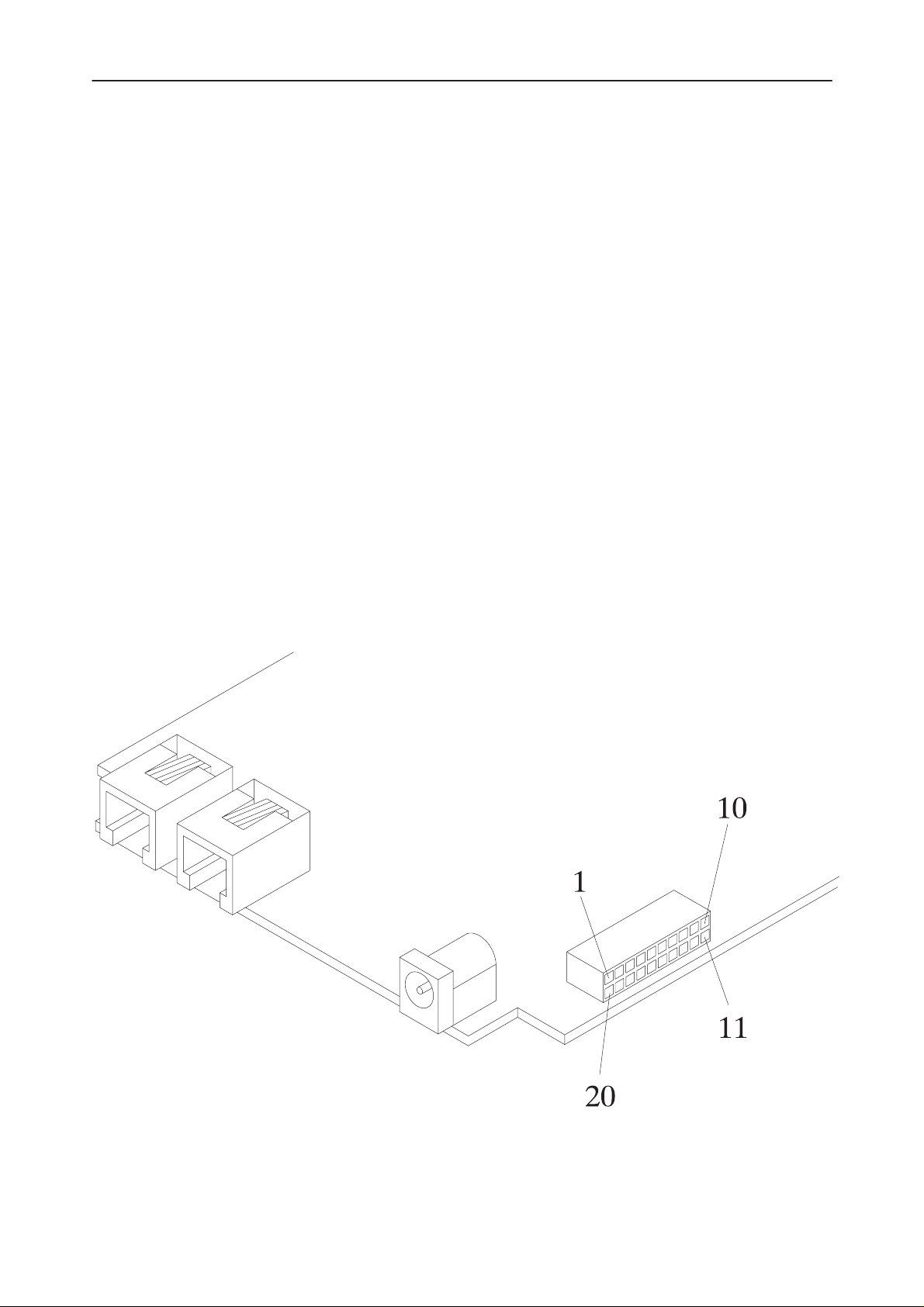
WT3 is the baseband/RF module TFK–1 cellular transceiver. The WT3 module
carries out all the system and RF functions of the transceiver. The system module WT3 is designed for a WLL terminal, that operate in the PCN system.
Technical Section
All functional blocks of the system module are mounted on a single multi layer
printed circuit board. The chassis of the radio unit has separating walls for
baseband and RF. The connections to accessories are taken through the system connector of the radio unit. There is no physical connector between the RF
and baseband sections.
External Connections
The system module has two connectors, an external system connector, and
SIM connector.
Technical Documentation
System Connector X120
Page 4–4
Original 34/96
Page 5

After Sales
TFK–1
Technical Documentation
Accessory Connector
Pin: Name: Description:
1 RS_RX Serial RX (Receive data for serial communica–
2 RS_TX Serial TX (Transmit data for serial communica–
3 SCK_RTS Serial Clock (Serial Clock for synchronous
4 WDDIS • ”0”; min/max 0...0.6 V Watchdog disable,
System Module
tion)
• ”0”; min/max 0...0.6 V
• ”1”; min/max 2.4...3.2 V
tion)
• ”0”; min/max 0...0.6 V
• ”1”; min/max 2.4...3.2 V
communication / RS_RTS)
• ”0”; min/max 0...0.6 V
• ”1”; min/max 2.4...3.2 V
Flash mode
• ”1”; min/max 2.4...7.15 V, Normal mode
5 PCMDCLK Audio Clock (512 kHz) clock for audio data
• ”0”; min/max 0...0.6 V
• ”1”; min/max 2.4...3.2 V
6 MBUS Serial control bus (General Purpose Control
and Test Control Bus)
• ”0”; min/max 0...0.5 V
• ”1”; min/max 2.4...3.2 V
7 VPP Programming Voltage (Programming voltage is
applied before entering the programming state)
• active; min/max 11.6...12.6 V
• inactive; min/max 0...3.2 V
8 DBUS_RXD DBUS Interface (Receive data for DAI)
• ”0”; min/max 0...0.6 V
• ”1”; min/max 2.4...3.2 V
9 DBUS_TXD DBUS Interface (Transmit data for DAI)
• ”0”; min/max 0...0.6 V
• ”1”; min/max 2.4...3.2 V
10 PCMSCLK Audio Clock (8 kHz slot clock for audio data)
• ”0”; min/max 0...0.6 V
• ”1”; min/max 2.4...3.2 V
11 VL Logic Supply Voltage (3 V Logic voltage)
12 FBUS_TX FBUS TX (FBUS transmit)
Original 34/96
• typical; 3.2 V
• ”0”; min/max 0...0.5 V
• ”1”; min/max 2.4...3.2 V
Page 4–5
Page 6

TFK–1
After Sales
System Module
Pin: Name: Description:
13 FBUS_RX FBUS RX
14 VBATT Battery supply voltage
15 DGND Digital ground
16 RS_CTS RS232 (Handshake signal for RS–232 serial
17 HOOK_DTR Accessory detection
18 AGND Analog ground
19 XMIC_ID External Microphone Input (Audio in e.g. ser-
vice handset)
Technical Documentation
• FBUS receive ”0”; min/max 0...0.6 V
• Pull–up on base band ”1”; min/max 2.4...3.2 V
• min/max 6.45...7.15 V
interface)
• active; min/max 0...0.5 V
• inactive; min/max 2.4...3.2 V
• typical 200 mV
20 XEAR_DSR External Speaker (Audio out e.g. service
SIM Connector X300
Pin: Name: Description:
1 GND Ground for SIM
2 VSIM SIM voltage supply
3 SDATA Serial data for SIM
4 SRES Reset for SIM
5 CLK Clock for SIM data (clock frequency minimum
handset)
• min/typ/max: 4.8...4.9...5.0 V
1 MHz if clock stopping not allowed)
Page 4–6
Original 34/96
Page 7

After Sales
TFK–1
Technical Documentation
Baseband Block
Introduction
The WT3 module is used in TFK–1 products. The baseband is built around one
DSP, System ASIC and the MCU. The DSP performs all speech and GSM/PCN
related signal processing tasks. The baseband power supply is 3V, except for
the A/D and D/A converters that are the interface to the RF section, and to the
comparators in the LAPWRU.
The audio codec is a separate device which is connected to both the DSP and
the MCU. The audio codec supports the internal audio from line adapter and
external audio from the service handset.
The baseband clock reference is derived from the RF section, and the reference frequency is 13 MHz. A low level sinusoidal wave form is fed to the ASIC
which acts as the clock distribution circuit. The DSP is running at 39 MHz using
an internal PLL. The clock frequency supplied to the DSP is 13 MHz. The MCU
bus frequency is the same as the input frequency. The system ASIC provides
both 13 MHz and 6.5 MHz as alternative frequencies. The MCU clock frequency is programmable by the MCU. The baseband uses 13 MHz as the MCU operating frequency. The RF A/D, D/A converters are operated using the 13 MHz
clock supplied from the system ASIC
System Module
The power supply IC contains three different regulators. The output voltage
from each regulator is 3.15V nominal. One of the regulators uses an external
transistor as the boost transistor.
Original 34/96
Page 4–7
Page 8
TFK–1
After Sales
System Module
Modes of Operation
The baseband can operate only in the active mode in WLL terminal.
Circuit Description
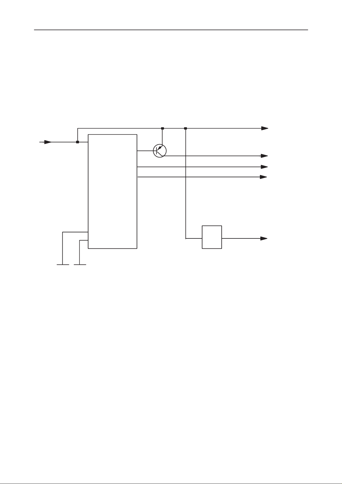
Power Supply
+6.6 V
5,21,44,39,37
VBAT
N300
43
35
40
V300
Technical Documentation
VBATT
+6.6 V
VL +3.2V
VA +3.2 V
VSL +3.2 V
DGND
4,20,38
6,32
AGND
The baseband has one power supply circuit N300 delivering power to the different parts in the baseband. There are two logic power supplies and one analog
power supply. The analog power supply VA is used for analog circuits such as
audio codec. Due to the current consumption and the baseband architecture
the digital supply is divided into to parts.
Both digital power supply VSL and VL from the N300 PSCLD are used to distribute the power dissipation inside N300 PSCLD. The main logic power supply
VL has an external power transistor, V300 to handle the power dissipation.
D400, ASIC, and the MCU SRAM D440 are connected to the same logic supply
voltage. All other digital circuits are connected to the main digital supply. The
analog voltage supply is connected to the audio codec.
N350
VCC
+5.0 V
Page 4–8
Original 34/96
Page 9

After Sales
TFK–1
Technical Documentation
Power Supply Regulator PSCLD, N300
The power supply regulators are integrated into the same circuit N300. The
power supply IC contains three different regulators. The main digital power supply regulator is implemented using an external power transistor V300. The other two regulators are completely integrated into N300.
PSCLD, N300 External Components
N300 performs the required power–on timing. The PSCLD N300 internal power on and reset timing is defined by the external capacitor C318. This capacitor
determines the internal reset delay, which is applied when the PSCLD N300 is
initially powered by applying the power supply. The baseband power–on delay
is determined by C315. With a value of 10 nF, the power–on delay after a power–on request has been active is in the range of 50–150 ms. C311 determines
the PSCLD N300 internal oscillator frequency, and the minimum power–off
time when power is switched off.
The sleep control signal from the ASIC D400 is connected via PSCLD N300.
During normal operation, the baseband sleep function is controlled by the ASIC
D400, but since the ASIC is not powered up during the startup phase, the sleep
signal is controlled by PSCLD N300 as long as the PURX signal is active. This
arrangement ensures that the 13 MHz clock provided from RF to the ASIC
D400 is started and stable before the PURX signal is released, and the baseband exits reset. When PURX is inactive high, the sleep control signal is controlled by the ASIC D400.
System Module
N300 requires capacitors on the input power supply as well as on the output
from each regulator to keep each regulator stable during different load and temperature conditions. Due to EMC precautions, a filter using C301, L302 and
L303 has been inserted into the supply rail. This filter reduces the high frequency components present at the VBAT from exiting the baseband into the power
supply. The regulator outputs also have filter capacitors for power supply filtering and regulator stability. A set of different capacitors are used to achieve a
high bandwidth in the suppression filter.
PSCLD, N300 Control Bus
The PSCLD, N300 is connected to the baseband common serial control bus.
This bus is a serial control bus from the ASIC D400 to several devices on the
baseband. This bus is used by the MCU to control the operation of N300 and
other devices connected to the bus. N300 has two internal 8 bit registers and
the PWM register used for charging control. The registers contain information
for controlling reset levels, charging HW limits, watchdog timer length, and
watchdog acknowledgement.
The control bus includes three wires: clock, serial data, and chip select for each
device on the bus. From the PSCLD N300 point of view, the bus can be used
for writing only. It is not possible to read data from PSCLD N300 by using this
bus.
Original 34/96
Page 4–9
Page 10

TFK–1
After Sales
System Module
The MCU can program the HW reset levels when the baseband exits/enters reset. The programmed values are retained until PSCLD N300 is powered off,
i.e. the power supply is cut off. At initial power–on, when PSCLD is powered–
on, the default reset level is used. The default value is 5.1 V, with the default
hysteresis of 400 mV. This means that reset is exit at 5.5 V when the PSCLD
N300 is powered for the first time.
The watchdog timer length can be programmed by the MCU using the serial
control bus. The default watchdog time is 32 s with a 50 % tolerance. The complete baseband is reset if the watchdog is not acknowledged within the specified time. The watchdog is running while PSCLD N300 is powering–up the system but PURX is active. This arrangement ensures that if for any reason the
supply voltage doesn’t increase above the reset level within the watchdog time
the system is reset by the watchdog. As the time PURX is active is not exactly
known, and depends upon startup conditions, the watchdog is internally acknowledged in PSCLD when PURX is released. This gives the MCU always the
same time to respond to the first watchdog acknowledge.
The PSCLD N300 also contains a switch for connecting and the supply voltage
to the baseband A/D converters. The switch state can be changed by the MCU
via the serial control bus. When PURX is active, the switch is open to prevent
the supply voltage from being applied to the baseband measurement circuitry,
which is powered off. Before any measurement can be performed, the switch
must be closed by MCU.
Technical Documentation
SIM Interface and Regulator in N300
The SIM card regulator and interface circuit is integrated into PSCLD N300.
The benefit from this is that the interface circuits are operating from the same
supply voltage as the card, avoiding the voltage drop caused by the external
switch used in previous designs. The PSCLD N300 SIM interface also acts as
voltage level shifting between the SIM interface in the ASIC D400 operating at
3V and the card operating at 5V. Interface control in PSCLD is direct from
ASIC, D400 SIM interface. The MCU can select the power supply voltage for
the SIM using the serial control bus. The default value is 3V which needs to be
changed to 5V before power–up of the SIM interface in ASIC D400. The regulator enable and disable is controlled by the ASIC via SIMI(2).
Page 4–10
Original 34/96
Page 11
After Sales
TFK–1
Technical Documentation
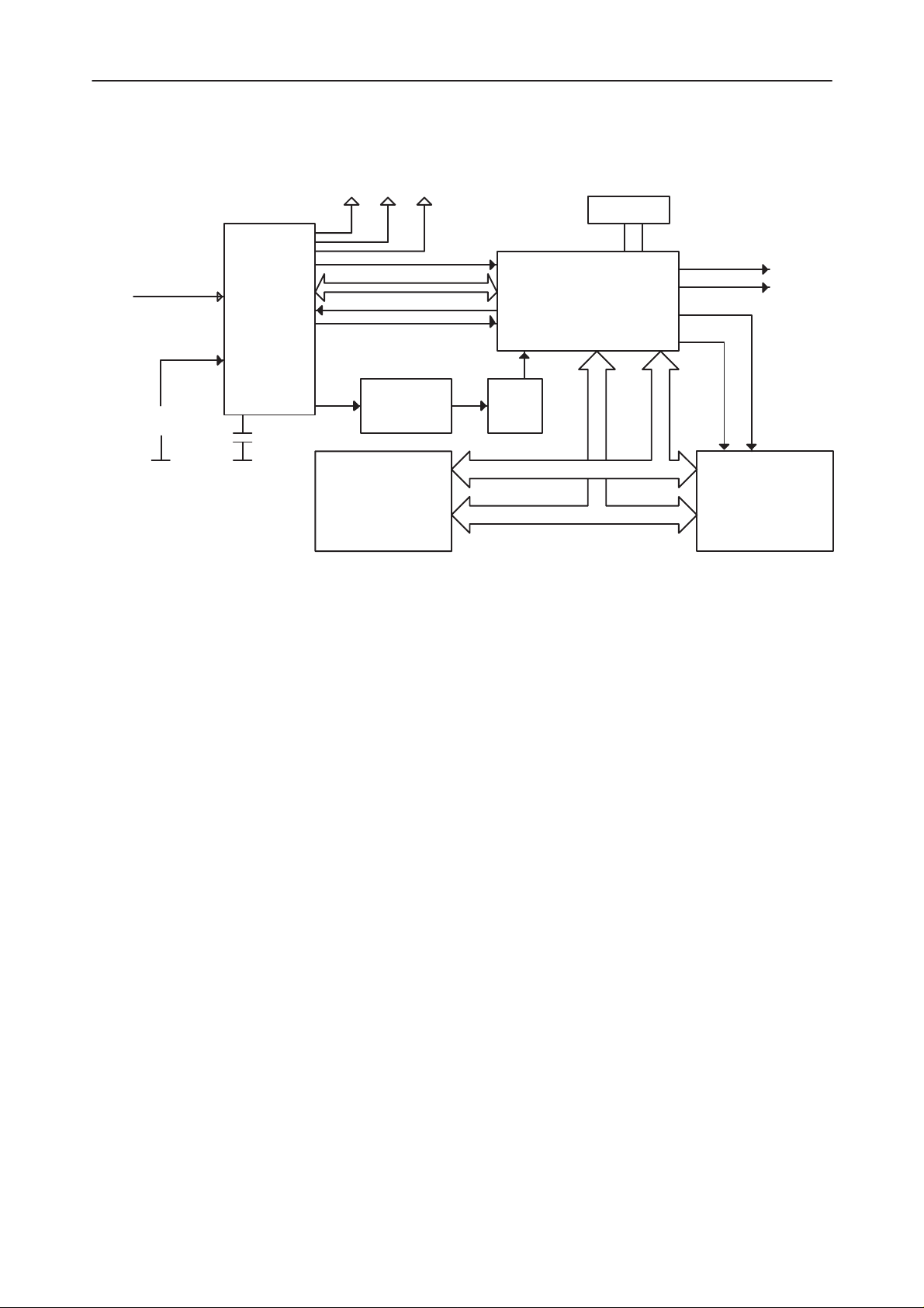
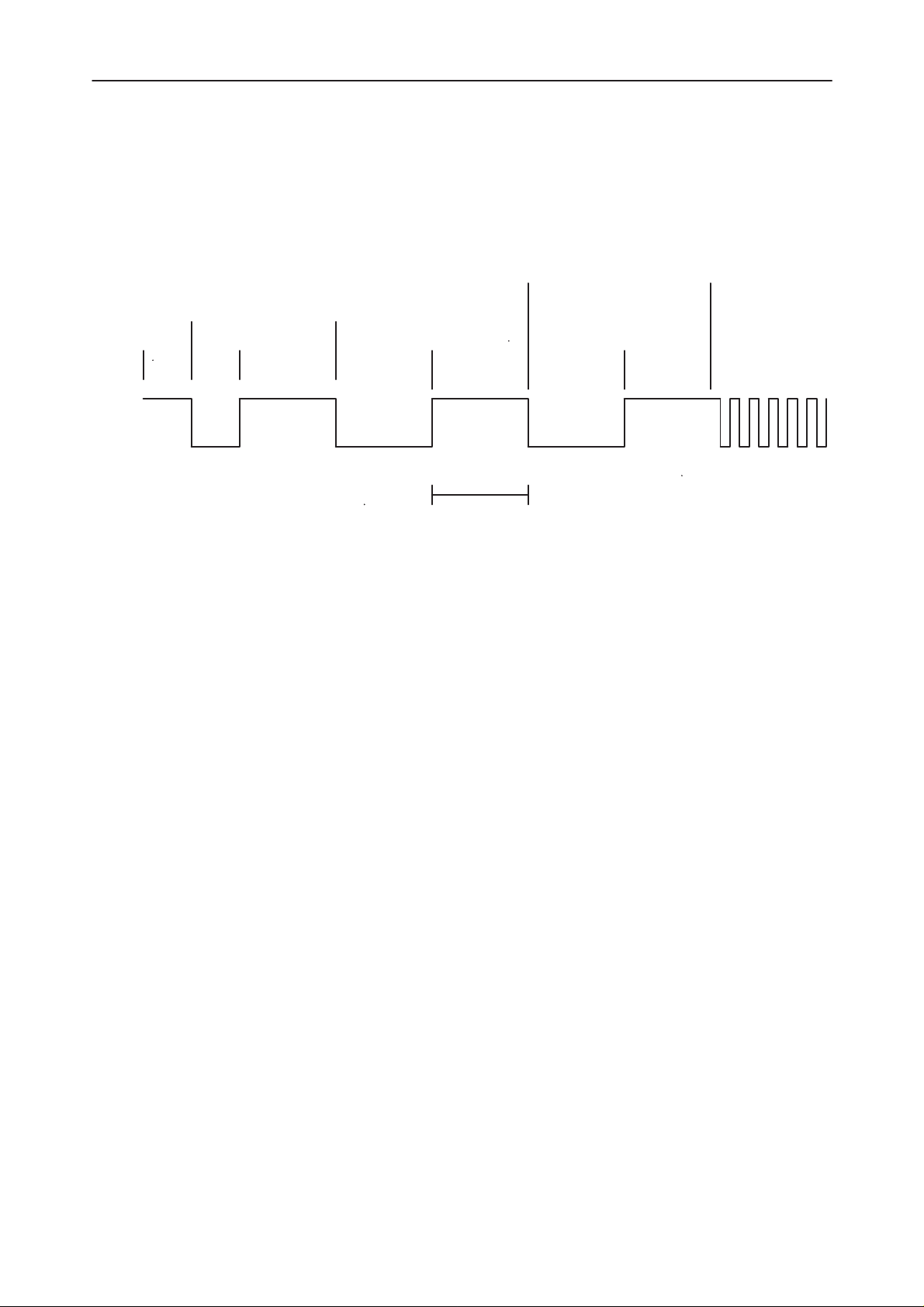
Power–Up Sequence
PSCLD
N300
VBAT
Watchdog
disable
5,21,37
39,44
25
23
28
30
16,18,19
C310
VL VSL VA
40
35
26 120
17 130
14
13
CRFCONT
N601
Purx
Serial Bus
VCXO Enable
CHARGAlarm
1415
129
VCXO
SRAM, FLASH
D440 D430
22
13 MHz
Address Bus
ASIC
D400
Watchdog
Register
32 kHz
125 126
Data Bus
System Module
83
84
MCU Clock
82
MCU Reset
81
48 51
DSP Reset
DSP Clock
MCU
D420
Power–On Reset Operation
The system power–up reset is generated by the regulator IC N300. The reset
is connected to the ASIC D400 that is reset whenever the reset signal PURX is
low. The ASIC D400 then resets the DSP D360, the MCU D420, and the digital parts in N450. When reset is removed, the clock supplied to the ASIC D400
is enabled inside the ASIC. At this point the 32 kHz oscillator signal is not enabled inside the ASIC, since the oscillator is still in the startup phase. To start
up the block requiring 32 kHz clock, the MCU must enable the 32 kHz clock.
The MCU reset counter is now started and the MCU reset is still kept active
low. A 6.5 MHz clock is started to MCU in order to put the MCU D420 into reset. The MCU is a synchronous reset device and needs a clock to reset. The
reset to MCU is set inactive after 128 MCU clock cycles, and MCU is started.
DSP D360 and N450 reset is kept active when the clock inside the ASIC D400
is started. A13 MHz clock is started to DSP D360 and puts it into reset. D360
is a synchronous reset device, and requires a clock to enter reset. The N450
digital parts are reset asynchronously and do not need a clock to be supported
to enter reset.
As both the MCU D420 and DSP D360 are synchronous reset devices, all interface signals connected between these devices and ASIC D400 which are
used as I/O are set into input mode on the ASIC D400 side during reset. This
avoids bus conflicts occurring before the MCU D420 and the DSP D360 are
actually reset.
The DSP D360 and N450 reset signal remains active after that the MCU has
exited reset. The MCU writes to the ASIC register to disable the DSP reset.
This arrangement allows the MCU to reset the DSP D360 and N450 whenever
Original 34/96
Page 4–11
Page 12

TFK–1
After Sales
System Module
needed. The MCU can put DSP into reset by writing the reset active in the
ASIC D400 register
MCU
The baseband uses a Hitachi H3001 type of MCU. This is a 16–bit internal
MCU with 8–bit external data bus. The MCU is capable of addressing up to 16
MByte of memory space linearly, depending upon the mode of operation. The
MCU has a non multiplexed address/data bus which means that memory access can be done using less clock cycles thus improving the performance but
also tightening up memory access requirements. The MCU is used in mode 3
which means 8–bit external data bus and 16 Mbyte of address space. The
MCU operating frequency is equal to the supplied clock frequency. The MCU
has 512 bytes of internal SRAM. The MCU has one serial channel, USART that
can operate in synchronous and asynchronous mode. The USART is used in
the MBUS implementation. The clock required for the USART is generated by
the internal baud rate generator. The MCU has 5 internal timers that can be
used for timing generation. Timer TIOCA0 input pin 71 is used for generation of
netfree signal from the MBUS receive signal which is connected to the MCU
USART receiver input on pin 2.
Technical Documentation
The MCU contains 4 10–bit A/D converters channels that are used for baseband monitoring.
The MCU, D420 has several programmable I/O ports which can be configured
by SW. In this case, the data bus lines D0–D7 are used for baseband control
functions. It is not used as part of the data bus.
MCU Access and Wait State Generation
The MCU can access external devices in 2 state access or 3 state access. In
two state access the MCU uses two clock cycles to access data from the external device In 3 state access the MCU uses 3 clock cycles to access the external device or more if wait states are enabled. The wait state controller can operate in different modes. In this case, the programmable wait mode is used.
This means that the programmed amount of wait states in the wait control register are inserted when an access is performed to a device located in that area.
The complete address space is divided into 8 areas each area covering 2
MByte of address space. The access type for each area can be set by bits in
the access state control register. Furthermore, the wait state function can be
enabled separately for each area by the wait state controller enable register.
This means that in 3 state access, two types of access can be performed with a
fixed setting:
Page 4–12
– 3 state access without wait states
– 3 state access with the amount of wait states inserted determined by the
wait control register
Original 34/96
Page 13

After Sales
TFK–1
Technical Documentation
If the wait state controller is not enabled for a 3 state access area, no wait
states are inserted when accessing that area even if the wait control register
contains a value that differs from 0 states.
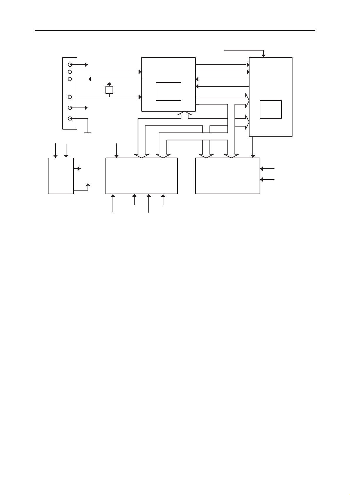
MCU Flash Loading
The flash loading equipment is connected to the baseband by means of the
service adapter. The power supply for the baseband is supplied via the adapter
and controlled by the flash programming equipment. The baseband module is
powered up when the power is connected to the power supply connector.
Five signals are required for the flash programming, with the addition of the
power supply. The baseband MCU will automatically wait for flash down–loading to be performed if one of the two following criteria are met.
– The flash is found to be empty when tested by the MCU
– The serial clock line at the baseband MCU is forced low when the MCU is
exiting reset
The second alternative is used for reprogramming as the flash is not empty in
this case. To allow the serial clock line to be forced low during MCU initial boot
there is a requirement that the flash prommer can control the power on of the
baseband module. This is done by controlling the switching of the power supply. This arrangement allows the baseband module to operate in normal mode
even if the flash prommer is connected but not active. The flash prommer also
disables the power supply watchdog during flash programming to prevent unwanted reset of the baseband. The programming voltage to the flash is applied
when the flash prommer has detected that the baseband module is powered.
This detection is performed by monitoring the serial interface RS_RX line from
the baseband. The RS_RX line is pulled high by a pull–up resistor in idle. The
VPP voltage is set to 5V as it is not known at this point what type of device is
used.
System Module
The following diagram shows the block diagram for the baseband flash programming circuitry.
Original 34/96
Page 4–13
Page 14
TFK–1
After Sales
System Module
X120
7
VPP
1
RS_RX
2
RS_TX
3
SCK_RTS
4
WDDis
15
GND
VBAT
Flash Prommer
5... 22
PSCLD
N301
26
VL,VSL
40
FLASH pin11 Vpp
PSCLD pin 22 WDDis
GND
Programming Voltage Vpp
ASIC pin 120
PurX
ASIC pin 130 PwrDown
VLC
R436
11
FLASH
D430
ASIC pin 51 CSelX
2,71
1
3
MCU pin 55 RdX
MCU
D420
Internal
RAM
38(9)37(24)9(24)12(10)
MCU pin 56 WrX
Technical Documentation
PSCLD pin 26 PurX
Master Reset
56
55
MCUResX
51 82
MCUClk
MCUAdrress
MCUData
WrX
RdX
SRAM
D440
55
56
8148
49
RAMCSelX
30
5
32
120
ASIC
D400
BOOT
ROM
MCU pin 56 WrX
MCU pin 55 RdX
The interface lines between the flash prommer and the baseband are in low
state when power is not connected by the flash prommer. The data transfer between the flash programming equipment and the base band is synchronous,
and the clock is generated by the flash prommer. The same MCU USART that
is used for MBUS communication is used for the serial synchronous communication. The PSCLD watchdog is disabled when the service adapter and flash
prommer are connected.
After the service adapter has been connected to the board the power to the
baseband module can be connected by the flash prommer or the test equipment. All interface lines are kept low, except for the data transmit from the
baseband that is in reception mode on the flash prommer side, this signal is
called RS_TX. The MCU boots from ASIC and investigates the status of the
synchronous clock line. If the clock input line from the flash prommer is low or
no valid SW is located in the flash, MCU forces the initially high RS_TX line low
acknowledging to the flash prommer that it is ready to accept data.
The flash prommer sends data length, 2 bytes, on the RS_RX data line to the
baseband. The MCU acknowledges the 2 data byte reception by pulling the
RS_TX line high. The flash prommer now transmits the data on the RS_RX line
to the MCU. The MCU loads the data into the internal SRAM. After having received the transferred data correctly MCU puts the RS_TX line low and jumps
into internal SRAM and starts to execute the code. After a guard time of 1 ms
the RS_TX line is put high by the MCU. After 1 ms the RS_TX is put low indicating that the external SRAM test is going on. After a further 1 ms, the RS_TX
is put high indicating that external SRAM test has passed. The MCU performs
Page 4–14
Original 34/96
Page 15
After Sales
TFK–1
Technical Documentation
the flash memory identification based upon the identifiers specified in the Flash
Programming Specifications. In case of an empty device, identifier locations
shows FFH, the flash device code is read and transmitted to the Flash Prommer.
Internal SRAM
Reset
RS_TX
Boot OK
Length OK
execution begin External SRAM
External SRAM
test going on
1 ms
System Module
Ready to send
Flash ID
test passed
After that, the device mounted on baseband has been identified, and the Flash
Prommer down–loads the appropriate algorithm to the baseband. The programming algorithm is stored in the external SRAM on the baseband module,
and after having down–loaded the algorithm and data transfer SW, the MCU
jumps to the external SRAM and starts to execute the code.
The MCU now asks the prommer to connect the flash programming power supply. This SW loads the data to be programmed into the flash, and implements
the programming algorithm that has been down loaded.
Flash, D430
A 8 MBit Boot Block flash is used as the main program memory D430. The device is 3 V read/program with external 12V VPP for programming. The device
has a lockable boot sector. This function is not used since the complete code is
reprogrammed. The Boot sector is located at the ”bottom”, definition by Intel,
address 00000H–03FFFH. The block is unlocked by a logic high state on pin
12. This logic high level is generated from VPP. The device can be programmed by a VPP of 5V but the programming procedure takes longer. To improve programming, the programming voltage used is 12V. The speed of the
device is 150 ns. The MCU operating at 6.5 MHz will access the flash in 2 state
access, requiring 150 ns access time from the memory.
SRAM D440
The baseband is designed to take two different size of SRAMs, 64kx8 and
128kx8, not at the same time. The required speed is 150 ns as the MCU will
operate at 6.5 MHz and the SRAM will be accessed in 2 state access. The
SRAM has no battery backup which means that the content is lost even during
Original 34/96
Page 4–15
Page 16

TFK–1
After Sales
System Module
short power supply disconnections. As shown in the memory map, the SRAM is
not accessible after boot until the MCU has enabled the SRAM access by writing to the ASIC register.
EEPROM D445
The baseband is designed to take an 2kx8 serial EEPROM. TFK–1 will use the
2kx8 serial device over the I2C bus. The I2C bus protocol is implemented in
SW and the physical implementation is performed on MCU Port 4.
MCU and Peripherals
MCU Port P4 Usage
MCU, D420 port 4 is used for baseband control.
Port Pin MCU pin Control Function Remark
P40 5 SLIC–CTRL 0
P41 6 SLIC–CTRL 1
Technical Documentation
P42 7 SLIC–CTRL 2
P43 8 RS_DSR
P44 9 EEPROM SCK
P45 10 EEPROM SDA
P46 11 EEPROM write enable Active low
P47 12 RS_CTS
Baseband A/D Converter Channels usage in N450 and D420
The auxiliary A/D converter channels inside RFI2 N450 are used only for measuring of the system board temperature by the MCU.
The MCU has 4 10 bit A/D channels which are used for baseband voltage monitoring. The MCU can measure supply voltage, accessory detection (ID), loop
current (IBBDET) and loop voltage (VBBDET) by using it‘s own converters.
Page 4–16
Original 34/96
Page 17

After Sales
TFK–1
Technical Documentation
Baseband N450 A/D Converter Channel Usage
Name: Usage: Input volt. range
Chan 0 System board temperature 0...3.2 V
Chan 1–7 not used
MCU Baseband A/D Converter Channel Usage
Name: Usage: Input volt. range
Chan 0 Supply voltage 0...3.2 V
Chan 1 Accessory detection 0...3.2 V
Chan 2 IBBDET 0...3.2 V
Chan 3 VBBDET 0...3.2 V
Supply Voltage Measurement
The supply voltage is measured using MCU N420 A/D converter channel 0.
The supply voltage supplied to the A/D converter input is switched off when the
baseband is powered off. The supply voltage measurement voltage is supplied
by PSCLD N300, which performs switch–off, and scaling with a scaling factor
of R1(R1+R2). The measurement voltage is filtered by a capacitor to achieve
an average value that is not depending upon the current consumption behavior
of the baseband. To be able to measure the supply voltage during transmission
pulse, the time constant must be short. The value for the filtering capacitor is
set to 1 nF C319. The scaling factor used to scale the supply voltage must
be 1:3, which means that a 9V supply voltage will give 3V A/D converter input
voltage. The A/D converter value in decimal can be calculated using the following formula:
System Module
A/D = 1023xR1xU
where K is the scaling factor. K = R1/((R1+R2)xU
Audio Control
The audio codec N130 is controlled by the MCU D420. The ASIC generates a
512 kHz data clock, and a 8 kHz synchronization signal for the PCM data bus.
Data is put out on the bus at the rising edge of the clock and read in at the falling edge. Data from the DSP D360 to the audio codec N130 is transmitted as
a separate signal from data transmitted from the audio codec, N130 to the DSP
D360. The communication is full duplex synchronous. The transmission is
started at the falling edge of the synchronization pulse. 16 bits of data is transmitted after each synchronization pulse.
/((R1+R2)xU
BAT
) = 1023xU
ref
BAT
ref).
xK
Original 34/96
Page 4–17
Page 18
TFK–1
After Sales
System Module
LATX
C132
XEAR
LARX
C134
R133 C133
C135
14
8
6
25
24
CODEC
N130
CLK
CSX
DATA
11
12
13,16
23
22
20
19
10
17
C140
Serial Bus
AUDIO DATA IN
AUDIO DATA OUT
X120
SYSTEM
CONNECTOR
17
C137
CLK 512 kHz
SYNC 8 kHz
VLC
R113
Technical Documentation
MCU
D420
293727
3341
31
DSP
D360
EXT EQUIPM. INDICATION
R208
IRQ1X
68
Data, Addr Bus
A/D Converters
Data, Addr Bus
78
42,44,46
40
41
R115
MCU pin 64
ASIC
D400
122
The 512 kHz clock is generated from 13 MHz using a PLL type of approach,
which means that the output frequency varies as the PLL adjusts the frequency.
The average frequency is 512 kHz. The clock is not supplied to the codec when
it is not needed. The clock is controlled by both MCU and DSP. DTMF tones
are generated by the audio codec and for that purpose, the 512 kHz clock is
needed. The MCU must switch on the clock before the DTMF generation control data is transmitted on the serial control bus.
The serial control bus uses clock, data, and chip select to address the device
on the bus. This interface is built into the ASIC, and the MCU writes the destination and data to the ASIC registers. The serial communication is then initiated by the ASIC. Data can be read form the audio codec N130 via this bus.
Page 4–18
Original 34/96
Page 19

After Sales
TFK–1
Technical Documentation
DSP
The DSP used in TFK–1 is the TI 320LC546. This is a 16 bit DSP that can use
external and/or internal memory access. The DSP can operate in two modes
microprocessor mode or micro–controller mode. The difference between the
two modes is that in microprocessor mode the DSP boots from external
memory, while in the micro–controller mode the DSP boots from internal ROM.
The DSP external memory access is divided into data, program, and I/O access. The type of access is indicated on three control pins that can be used for
memory control.
The DSP D360 executes code from the internal ROM. The baseband also provides external memories for the DSP, D371, D372, D381, and D382 (Note:
These memories are not fitted in all transceivers). The DSP is capable of addressing 64 kword of memory. The memory area is divided into a code execution area and a data storage area. The code execution area is located at address 4000H–FFFFH in the internal ROM. The external memories are arranged
in such a way that the DSP can access the external memories both as data
storage and code execution. The memory chip select is taken from the memory
access strobe signal from the DSP. This means that the memory is active during any memory access. The SRAMs are configured in chip select controlled
write mode. This means that both the write signal and the output enable signal
are active at the same time, and the actual write occurs at the rising edge of the
chip select signal. This implementation is required since the DSP supports only
one signal for write/read control.
System Module
The DSP is operating from the 13 MHz clock. In order to get the required performance, the frequency is internally increased by a PLL by a factor of 3. The
PLL requires a settling time of 50 us after that the clock has been supplied before proper operation is established. This settling counter is inside the DSP although the ASIC D400 contains a counter that will delay the interrupt with a
programmable amount of clock cycles before the interrupt causing the clock to
be switched on is presented to the DSP. The DSP has full control over the clock
supplied to it. When the DSP is to enter the sleep mode the clock is switched
off by setting a bit in the ASIC register. The clock is automatically switched on
when an interrupt is generated.
The DSP also has two synchronous serial channels for communication. One
channel is used for data transmission between the DSP and the audio codec.
This channel is operating at 512 kbits, and clock and synchronization signal is
provided by the ASIC D400. The other channel is used for debugging purposes, and uses the same clock and synchronization signals. The DSP has an
interrupt controller servicing four interrupts and one non maskable interrupt,
NMI. The interrupts have fixed priority which can only be changed by changing
the interconnection between the interrupt sources by HW
The ASIC contains DSP support functions as modulator, encryption/decryption
using algorithms A5/A51, RF power ramp generation/AGC control, AFC control,
synthesizer serial interface, frame counters, timer, RFI2 interface, and RX and
TX power control timing. The RF power ramp timing/AGC control, AFC control,
.
Original 34/96
Page 4–19
Page 20

TFK–1
After Sales
System Module
and synthesizer control are timed to the value of the frame counter. This means
that data is loaded into the registers, and transferred when the frame counter
and the reference values match. This allows timing of the synthesizer control
power ramp and start of TX data to be controlled very precisely.
As the receiver and the transmitter is not operating at the same time, the TX
power ramp function is used to control the AGC in the receiver during the reception. This requires the DSP to continuously modify the values in the TX
ramp SRAM to fit the ramp during TX and the AGC value during reception.
DSP ASIC Access
The DSP is accessing the ASIC in the DSP I/O area. 2 wait states are required
for the ASIC access. Some of the DSP registers located in the ASIC are retimed to the internal ASIC clock and requires special handling with respect to
consecutive writing. This means that the same register can not be written again
until a specified time has passed. To cope with this, DSP is inserting NOP
instructions to satisfy this requirement.
DSP Interrupts
Technical Documentation
The DSP supports 4 external interrupts. Three interrupts are used. The ASIC,
D400 generates two of the interrupts. One interrupt is generated by the RFI2
N450 auxiliary A/D converter. This interrupt is generated when a baseband
measurement A/D conversion is completed. The interrupts to the DSP are active low.
INT0, which is the highest priority interrupt, is used for data reception from the
receiver and is generated by the ASIC. The INT1 signal is used for auxiliary
A/D channel conversions generated by the RFI2. This interrupt is generated by
RFI2 and is a result of measurement requests from the DSP. INT3 is a low
priority interrupt generated by the ASIC timer. The DSP programs the timer value and an interrupt is given when the timer expires. The interrupt must be active at least 1 DSP clock cycle as it is sampled on the rising/falling edge by the
DSP. All interrupts are active low.
Unused interrupt controller inputs are tied high.
DSP Serial Communications Interface
The DSP contains two synchronous serial communications interfaces. One of
the interfaces is used to communicate with the audio codec N130. The 512
kHz clock required for the data transfer is provided by D400 as well as the 8
kHz synchronization signal. Data is transferred on to lines, RX and TX creating
a full duplex connection. Data is presented on the bus on the first rising edge of
the clock after the falling edge of the synchronization pulse. Data is read in by
each device on the falling edge of the clock. Data transfer is 16 bits after each
synchronization pulse.
Page 4–20
Original 34/96
Page 21

After Sales
TFK–1
Technical Documentation
The DSP D360 has control over the clock provided to the audio codec. The
DSP can switch on the clock to start the communication, and switch it off when
it is not needed. This clock is also under control of MCU D420.
RF Synthesizer Control
The synthesizer control is performed by the DSP D360 using the ASIC D400
as the interfacing and timing device. Different synthesizer interfaces are supported, and the required interface can be selected by the DSP at the initialization stage of the ASIC. The synthesizer interface also includes timing registers
for programming synthesizer data. The DSP loads the synthesizer data into the
transmission registers in the ASIC synthesizer interface together with the timing
information. The system timing information is used for synthesizer data loading.
When the system timing register, frame counter, value matches the timing value
programmed into the synthesizer interface, the interface transmits the loaded
data to the RF synthesizer, and the VCO frequency is changed accordingly. As
the synthesizer may be powered off when not needed, the interface pins towards the synthesizer can be put in tri–state or forced low when the interface is
not active.
System Module
RFI2 N450 Operation
The RFI2 N450 contains the A/D and D/A converters to perform the A/D conversion from the received signal and the D/A converters to perform the conversion for the modulated signal to be supplied to the transmitter section. In addition, the RFI2 chip also contains the D/A converter for providing AFC voltage to
the RF section. This AFC voltage controls the frequency of the 13 MHz VCXO
which supplies the system clock to the baseband. The RFI2 N450 also contains
the D/A converter to control the RF transmitter power control. The power control values are stored in the ASIC D400 and at the start of each transmission,
the values are read from the ASIC D400 to the D/A converter producing the
power control pulse. This D/A converter is used during the reception to provide
AGC for the receiver RF parts.
The RFI2 contains the interface between the baseband and the RF. The RFI2
circuit contains the A/D converters required for the receiver and the D/A converters required for the transmission. In addition, the RFI2 contains a 10 bit D/A
converter for AFC control, and one of the receiver A/D converters has a multiplexed input for 8 additional channels used for baseband monitoring functions.
The A/D converters are 12 bit sigma delta type. This means that the digital output is centered around the reference voltage and the output value is both negative and positive. The RFI2 has an internal reference voltage for the A/D and
D/A converters that can be switched off to save power. The reference has external filtering capacitors to improve the converter performance. The transmitter
D/A converters are followed by interpolator and post filter. The filter is of switch
capacitor type and the filter parameters are taken into account when modulator
parameters are calculated. The AFC D/A converter is static and requires no
Original 34/96
Page 4–21
Page 22

TFK–1
After Sales
System Module
clock for operation. This means that the RFI2 clock can be switched off and the
AFC value will be kept.
One of the A/D converters used for receiver signal conversion can be used as
an auxiliary converter that supplies 8 channels for baseband measurement purposes. When the converter is used in this mode, each conversion generates an
interrupt directly to the DSP. The DSP operates this converter via the ASIC
D400.
Data communication between the ASIC D400 and RFI2 N450 is carried out on
a 12 bit parallel data bus. The ASIC D400 uses 4 address lines to access RFI2
N450. Depending on the direction of the communication, either the write control
signal is used to write data to RFI2 N450 or the read signal is used to read
data from RFI2 N450. The ASIC D400 supplies 13 MHz clock to the RFI2
N450. This clock is used as reference for the A/D and D/A converters. Communication between the ASIC D400 and the RFI2 N450 is related to the clock.
The auxiliary channels supported by the RFI2 uses one of the receiver A/D
converters as the A/D converter. Due to the type of converter used for the receiver converters, the value read from the auxiliary channels can be negative.
The input voltage applied to the auxiliary channels must be within 0.5–3.0 V.
A 12 bit value is received from the auxiliary channel measurement. The auxiliary channel conversion complete is sent direct to the DSP as an interrupt, INT1.
The DSP reads the value using direct access through the ASIC to the RFI2
converter. The conversion is started by the DSP writing the address of the
channel to be measured to the ASIC register. The ASIC then writes the selected channel to RFI2, and the conversion is started. The DSP may sample
the same channel for more than one value as the A/D converter will produce
continuously new values. Several samples may be used for example in supply
voltage measurement to calculate an average value from the results.
Technical Documentation
The RFI2 N450 digital supply is taken from the baseband main digital supply.
The analog power supply, 4.5V is generated by a regulator supplied from the
RF section. The analog power supply is always supplied as long as the baseband is powered, if R311 is assembled. The RFI2 N450 analog power supply
can be switched off during sleep by removing R311 and adding R312. In this
case the RFI2 N450 analog power supply is in the control of the PSCLD N300
sleep control signal.
Receiver Timing and AGC
RF receiver power on timing is performed by the ASIC D400. The DSP D360,
can program the time when the receiver is to be powered on. The timing information is taken from the system timing that is based upon the frame counter
inside the ASIC D400, which is synchronized to the base station carrier frequency using AFC to tune the receiver. As transmission and reception takes
place at different times, the D/A converter used for transmitter power control is
used to control the AGC of the receiver during reception. This requires the DSP
D360 to alter the content of the SRAM containing the information that is written
to the D/A converter for the reception and the transmission.
Page 4–22
Original 34/96
Page 23

After Sales
TFK–1
Technical Documentation
RF Transmitter Timing and Power Control
The RF Power Amplifier (PA) timing control is performed by the ASIC D400.
The power control is performed by the ASIC D151 using the D/A converter in
N450. The ASIC D400 controls the power supply voltage to the RF transmitter
sections. As the first step, the relevant circuits are powered on using the TX
power control output from the ASIC D400. The timing for powering on the TX
circuits is generated from the ASIC internal system timing circuitry, frame counter. As the RF TX circuits need time to stabilize after power on before the actual
transmitter can be started, there is a programmable delay before the ASIC
D400 starts to write the power ramp data to the D/A converter inside N450. The
TXC signal which is generated in this way controls the power ramp of the PA
and the power level for that burst. At the end of the burst the power ramp is
written to the D/A converter inside N450. The data that creates the power ramp
and final power level is stored in a SRAM inside the ASIC D400. At the start of
the ramp, the contents of the SRAM are read out in increasing address order.
At the end of the ramp the contents are read out in decreasing address order.
The power level during the burst is determined by the last value in the SRAM,
this value is the value that will remain in the D/A converter during the burst. The
DSP D360 may change the shape of the falling slope of the power ramp by
writing new values to the power ramp SRAM during the burst.
System Module
As the transmitter may have to adjust the transmitter burst due to the distance
from the base station there is an additional timer for this purpose. This timing is
called the timing advance and will cause the transmission to start earlier when
the distance to the base station increases.
SIM Interface
The SIM interface is the serial interface between the smart card and the baseband. The SIM interface logic levels are 5V, since no 3V technology SIM is yet
available. The baseband is designed in such a way that a 3V technology SIM
can be used whenever it is available. The SIM interface signals are generated
inside the ASIC. The signals coming from the ASIC are converted to 5V levels.
The PSCLD circuit is used as the logic voltage conversion circuit for the SIM
interface. The PSCLD circuit also contains the voltage regulator for the SIM
power supply. The control signals from the ASIC to PSCLD are at 3V level and
the signals between PSCLD and the SIM are 5V levels. An additional control
line between the ASIC and the PSCLD is used to control the direction of the
DATA buffer between the SIM and the PSCLD. In a 3V technology environment
this signal is internal to the ASIC only. The pull up resistor required on the SIM
DATA line is integrated into the PSCLD, and the pull–up is connected to the
SIM regulator output inside PSCLD. In idle, the DATA line is kept as input by
both the SIM and the interface on the baseband. The pull–up resistor is keeping the DATA line in it’s high state.
The power up and power down sequences of the SIM interface are performed
according to ISO 7816–3. To protect the card from damage when the power
supply is removed during power on, there is a control signal, CARDIN, that au-
Original 34/96
Page 4–23
Page 24

TFK–1
After Sales
System Module
tomatically starts the power down sequence. The CARDIN information is taken
from 5 V regulator N350.
Since the power supply to the SIM is derived from PSCLD also using 3V
technology SIM, the power supply voltage of the SIM regulator is programmable 3.15/4.8 V. The voltage is selected by using the serial control bus to
PSCLD. The default value is set to 3.2V nominal.
For cross compatibility reasons, the interface should always be started up using
5V. The 3V technology SIM will operate at 5V but a 5V SIM will not operate at
3V. The supply voltage is switched to 3V if the SIM can accept that. The SIM
has a bit set in a data field indicating it’s capability of 3V operation.
The regulator control signal is derived from the ASIC, and this signal controls
the operation of the SIM power supply regulator inside PSCLD. To ensure that
the powered off ASIC doesn’t cause any uncontrolled operations at the SIM interface, the PSCLD signals to the SIM are forced low when the PURX signal is
active low. This implementation will ensure that the SIM interface can not be
activated by any external signal when PSCLD has PURX active. When PURX
goes inactive the control of the interface signals are given back to the ASIC signals controlling PSCLD SIM interface operations.
Technical Documentation
The clock to the SIM can be switched off if the SIM card allows stopping of the
clock. The clock can be stopped either in high or low state, determined by the
card data. For cards not allowing the clock to be stopped there is a 1.083 MHz
clock frequency that can be used to reduce the power consumption while the
clock is running. In this case the VCO must be running all the time. When the
clock is stopped, and the status of the CARDIN signal changes, power is
switched OFF, the clock to the SIM is restarted inside the ASIC, and the SIM
power down sequence is performed.
To be able to handle current spikes as specified in the SIM interface specifications, the SIM regulator output from PSCLD must have a ceramic capacitor of
100 nF connected between the output and ground close to the SIM interface
connector. To be able to cope with the fall time requirements and the disconnected contact measurements in type approval, the regulator output must be
actively pulled down when the regulator is switched off. This active pull–down
must work as long as the external battery is connected and the battery voltage
is above the PSCLD reset level.
The SIM power on procedure is controlled by the MCU. The MCU can power
up the SIM only if the CARDIN signal is in the inactive state low. Once the power up procedure has been started, the ASIC takes care that the power up procedure is performed according to ISO 7816–3.
Page 4–24
The SIM interface uses two clock frequencies 3.25 MHz or 1.625 MHz during
SIM communication. The data transfer speed in the SIM GSM session is specified to be the supplied clock frequency/372. The ASIC SIM interface supplies all
the required clock frequencies as well as the required clock frequency for the
UART used in the SIM interface data transmission/reception.
Original 34/96
Page 25

After Sales
TFK–1
Technical Documentation
Line Adapter
SWITCH
SEL1
tip1
tip2
ring1
ring2
SEL2
–VBB
tip
–VEE
LINE ADAPTER
ring
GND
–VCC
AGND
3
control bus
DET
IBBDET
audio in
audio out
RING_CLK
System Module
BB part
The Line Adapter makes 2 to 4–wire transformation between the termination
and the base part of the terminal. The 2–wire interface is of balanced line type,
and the voltage between tip and ring lines is about 40 V. The 4–wire part is a
normal audio–input (LATX) and audio–output (LARX) interface. The line Adapter is based on an Am79R79 SLIC circuit. It is controlled by the MCU with a 3 V
parallel bus (3 bits). SLIC uses three different states: ringing, active, and standby. The MCU can detect the termination state (ON–HOOK/OFF–HOOK) by the
DET pin. Ringing and metering are done via the RING_CLK line. In ringing
state, the MCU feeds 25 Hz to RINGIN pin. The circuit operates with three different operating voltages: VCC (+ 5 V), –VEE (– 5 V), and –VBB (– 50 V or –
60 V), and with two grounds GND and AGND. Loop current, Hook threshold,
and ring waveform are set by discrete components connected to circuits pins
RDC, RD, and RINGIN. Loop current can be detected with the IBBDET line,
which is connected to BB part.
The 2–wire line is divided to two separate 2 wire lines, tip1–ring1 (telephone),
and tip2–ring2 (fax machine). The divider is implemented with fet switches, and
both lines can be switched on or off separately. Control is made by the MCU
with SEL1 and SEL2 lines. Both 2 wire lines are protected by transient voltage
suppressors (82 V) connected from each line to ground.
Original 34/96
Page 4–25
Page 26

TFK–1
After Sales
System Module
Line Adapter Power Supply
Switching fet
VBAT
Current
buffer
Rectifier
Choke
Comparator
Filtering
Diff.amp
Technical Documentation
Current
limiting
–VBB
Regu–
lator
–VEE
Level
scaling
VBBDET
SWS_CLK
RING_CNTR
The Line Adapter power supply unit is of inverting switch mode power supply
type with PWM control. Voltage and current limitation are implemented in the
feedback. The main clock signal SWS_CLK is made by MCU, and it is 125 kHz
square wave. With RING_CNTR line output voltage can be increased from – 50
V to – 60 V when SLIC is in ringing state. The VBBDET line is used to detect
output voltage level. Current limitation is set to about 50 mA. The –VEE voltage
is provided by regulating from output voltage –VBB.
Page 4–26
Original 34/96
Page 27

After Sales
TFK–1
Technical Documentation
RF Block
Introduction
The RF module carries out all the RF functions of the transceiver. This module
works in the PCN system.
Components are located on one side of the PCB.
EMC leakage is prevented with magnesium shields. Shields conduct also heat
out of the inner parts of the phone, thus preventing excessive temperature rise.
Receiver
The receiver is a triple conversion receiver. There is also space diversity in this
receiver. Space diversity is created by using two separate RX antennas and
partially separate signal routes.
The received RF signal from the antenna is fed via a duplex filter or a separate
receiver filter to the receiver unit (see the block diagram). The signals are amplified by discrete low noise preamplifiers. The gain of the amplifiers and the
antenna selection are controlled by the ANT1 and ANT2 control lines. After the
preamplifier, the signal is filtered by a ceramic RX filter. The filter rejects spurious signals coming from the antenna, and spurious emissions coming from the
receiver unit.
System Module
The filtered RF– signal is down–converted by a passive diode mixer. The frequency of the first IF is 313 MHz. The first local signal is generated by the UHF
synthesizer. The IF signal is amplified, and then filtered by a microstripline filter. The filtered 1st IF is down–converted by the second mixer which is also a
passive diode mixer. The 2nd IF frequency is 87 MHz. The 2nd local signal is
generated by the VHF synthesizer.
The filtered IF signal is fed to the receiver part of the integrated RF circuit
CRFRT. In CRFRT, the filtered IF signal is amplified by an AGC amplifier which
has gain control range of 57 dB. The gain is controlled by an analog signal via
the TXC line. The amplified IF signal is down–converted to the last IF in the
mixer of CRFRT. The last local signal is generated from VHF VCO–signal by
dividing the original signal by four in the dividers of CRFRT.
The last IF frequency is 13 MHz. It is filtered by a ceramic filter. The filter rejects signals of the adjacent channels. The filtered last IF is fed back to CRFRT
where it is amplified and fed out to RFI via RXINN and RXINP lines.
Original 34/96
Page 4–27
Page 28

TFK–1
After Sales
System Module
Pre–Filters
The duplex filter consists of two functional parts; RX and TX filters. The TX filter
rejects the noise power in the RX frequency band and TX harmonic signals.
The RX filter rejects blocking and spurious signals coming from the antenna.
For diversity use, there is a separate RX filter, which rejects blocking and spurious signals coming from antenna 2.
Pre–Amplifier
The bipolar pre–amplifier amplifies the received signal coming from the antenna. In strong field conditions, the gain of the amplifier is reduced 24 dB, typically. The other pre–amplifier is for diversity use (ANT2).
Parameter
Frequency band:
Supply voltage (min/typ/max):
Current consumption (min/typ/max):
Technical Documentation
Value
1805–1880 MHz
4.27...4.5...4.73 V
6...8...10 mA
Insertion gain (min/typ/max): 13
Gain flatness: ±
Noise figure (typ/max):
Reverse isolation (min):
Gain reduction (min/typ/max):
IIP3: (min/typ):
Input VSWR; zo=50 Ω (max):
Output VSWR; zo=50 Ω (max):
RX Interstage Filter
The RX interstage filter is a three pole ceramic filter in PCN. The filter rejects
spurious and blocking signals coming from the antenna. It also rejects the local
oscillator signal leakage.
...15...17 dB
0.5 dB
2.1...2.5 dB
15 dB
21...24...27 dB
0...2.5 dBm
2.0
2.0
Page 4–28
Original 34/96
Page 29

After Sales
TFK–1
Technical Documentation
First Mixer
The first mixer is a single balanced passive diode mixer. The local signal is balanced by a printed circuit transformer. The mixer down–converts the received
RF signal to IF signal.
Parameter
RX frequency range:
LO frequency range:
IF frequency:
Conversion loss (min/typ/max):
IIP3 (min/typ):
LO – RF isolation (min):
LO power level (min):
First IF Amplifier
System Module
Value
1805–1880 MHz
1492–1567 MHz
313 MHz
5...6...7 dB
2...5 dBm
15.0 dB
3 dBm
The first IF amplifier is a bipolar transistor amplifier.
Parameter
Operation frequency:
Supply voltage (min/typ/max):
Current consumption (typ/max):
Insertion gain (min/typ/max):
Noise figure (typ/max):
IIP3 (min/typ):
First IF Filter
In PCN the first IF filter is a micro–stripline filter. The IF filter rejects some spurious and blocking signals coming from the front end of the receiver.
2nd Mixer
The 2nd mixer is a single balanced passive diode mixer. The local signal is balanced by a printed circuit transformer. The mixer down–converts the 1st IF signal 313 MHz to 2nd IF signal 87 MHz. I
Value
313 MHz
4.27...4.5...4.73
10...15 mA
11...13...15 dB
3...4 dB
–5...–3 dBm
= 20 mA.
C
2nd IF Amplifier
The 2nd IF amplifier is accomplished by using a resistive feedback connection
for the bipolar RF transistor. I
Original 34/96
= 13–14 mA.
C
Page 4–29
Page 30

TFK–1
After Sales
System Module
2nd IF Filter
The second IF filter (SAW) makes the part of the channel selectivity of the receiver. It rejects adjacent channel signals (except the 2nd adjacent). It also
rejects blocking signals, signals causing inter–modulation distortion, and the
3rd image frequency.
Receiver IF Circuit, RX part of CRFRT
The receiver part of CRFRT consists of an AGC amplifier with a 57 dB gain
control range, a mixer, and a buffer amplifier for the last IF. The mixer of the circuit down–converts the received signal to the last IF frequency. After external
filtering, the signals are amplified and fed differentially to the RFI circuit. The
supply current can be switched OFF by an internal switch, when the RX is OFF.
Parameter
Supply voltage (min/typ/max):
Current consumption (max):
Technical Documentation
Value
4.27...4.5...4.73 V
44 mA
Input frequency range (min/max):
Local frequency range of mixer
(min/max):
2nd IF range (min/max):
Voltage gain (max gain) of AGC
amplifier (min):
Noise figure (max):
AGC gain control slope (min/typ/max):
Mixer output 1 dB compression
point (typ):
Gain of the last IF buffer:
Max output level after last IF buffer (typ):
Last IF Filter
The last IF is 13 MHz. The ceramic filter on the last IF provides part of the
channel selectivity of the receiver.
45 MHz (–1 db point)
...87 MHz (–3 dB point)
42.5...100 MHz
2...17 MHz
47 dB
16 dB max gain
40...84...100 dB/V
1.0 V
PP
30 dB
1.6 V
PP
Transmitter
The TX intermediate frequency is modulated by an I/Q modulator contained in
the transmitter section of CRFRT IC. The TX I and Q signals are generated in
the RFI interface circuit, and they are fed differentially to the modulator.
Page 4–30
Original 34/96
Page 31

After Sales
TFK–1
Technical Documentation
Modulated intermediate signal is amplified or attenuated in temperature compensated controlled gain amplifier (TCGA). The output of the TCGA is amplified
and the output level is typically –15 dBm.
The output signal from CRFRT is low–pass filtered to reduce harmonics and
the final TX signal is achieved by mixing the UHF VCO signal and the modulated TX intermediate signal with passive mixer. After mixing, the TX signal is
amplified and filtered by two amplifiers and filters. These filters are dielectric filters. After these stages, the level of the signal is typically 1 mW (0 dBm) in
PCN.
The discrete power amplifier amplifies the TX signal to the desired power level.
The maximum output level at the antenna connector is typically 0.8...1.0 W.
The power control loop controls the output level of the power amplifier. The
power detector consists of a directional coupler and a diode rectifier. Transmitted power is controlled with controlled gain amplifier (TCGA) on the TX path
of CRFRT. The power is controlled with TXC and TXP signals. The power control signal (TXC), which has a raised cosine form, comes from the RF interface
circuit RFI.
System Module
Modulator Circuit TX, part of CRFRT
The modulator is a quadrature modulator contained in TX section of CRFRT IC.
The I and Q inputs generated by RFI interface are d.c. coupled and fed to the
modulator. The local signal is divided by two to get a 200 MHz modulating frequency. After mixing, the signals are combined and amplified with temperature
compensated controlled gain amplifier (TCGA). Gain is controlled with power
control signal (TXC). The output of the TCGA is amplified, and the maximum
output level is typically –10 dBm.
Parameter
Supply voltage (min/typ/max):
Supply current (max):
Local signal input
LO input frequency (min/max):
LO input power level (typ):
LO input resistance (min/typ/max):
Value
Value
4.27...4.5...4.73 V
35 mA
170...400 MHz
0.2 V
PP
70...100...130
Ω
LO input capacitance (typ):
Modulator Inputs (I/Q):
Input bias current, balanced (max):
Original 34/96
4 pF
Value
100 nA
Page 4–31
Page 32

TFK–1
After Sales
System Module
Input common mode voltage
(min/typ/max):
Input level, balanced (max):
Input frequency range (min/max):
Input resistance, balanced (min):
Input capacitance, balanced (max):
Modulator Output:
Output frequency (min/max):
Available linear RF power (typ):
Available saturated RF power (typ):
Total gain control range (min):
Gain control slope (typ):
Suppression of 3rd order prods (min):
Carrier suppression (typ):
Technical Documentation
2.05...2.2...2.4 V
1.1 V
PP
0...300 kHz
200 k
Ω
4 pF
Value
85...200 MHz
–10 dBm, ZiL=50 k
0 dBm, ZiL=50 k
Ω
45 dB
84 dB/V
35 dB
35 dB
Ω
Single sideband suppression:
Noise floor
Transmitted I/Q phase balance:
drift in whole temperature range:
Transmitted I/Q amplitude balance:
drift in whole temperature range:
Up–conversion Mixer
The up–conversion mixer is a single balanced passive diode mixer. The local
signal is balanced by a printed circuit transformer. The mixer up–converts the
modulated IF signal coming from quadrature modulator to RF signal.
Parameter:
TX frequency range:
LO frequency range:
IF frequency (nom):
Conversion loss (min/typ/max):
–135 dBm/Hz avg.
–5...5 deg
–2...2 deg
–0.5...0.5 dB
–0.2...0.2 dB
Value
1710...1785 MHz
1510...1585 MHz
200 MHz
6.0...7.0...8.0 dB
Page 4–32
IIP3 (min):
LO – RF isolation (min):
LO power level (max):
0.0 dBm
15 dB
3.0 dBm
Original 34/96
Page 33

After Sales
TFK–1
Technical Documentation
TX Interstage Filters
The TX filters reject the spurious signals generated in the up–conversion mixer.
They reject the local, image, and IF signal leakage, and RX band noise too.
1st TX Buffer
The TX buffer is a bipolar transistor amplifier. It amplifies the TX signal coming
from the up–conversion mixer.
Parameter:
Operating frequency range:
Supply voltage (min/typ/max):
Current consumption (typ/max):
Insertion gain (min/typ/max):
Input VSWR, Zo=50 Ω (max):
Output VSWR, Zo=50 Ω (max):
System Module
Value
1710...1785 MHz
4.25...4.5...2.8 V
4...5 mA
7...8...9 dB
2.0
2.0
2nd TX Buffer
The TX buffer is a bipolar transistor amplifier. It amplifies the TX signal coming
from the first interstage filter.
Parameter:
Operation frequency range:
Supply voltage (min/typ/max):
Current consumption (typ):
Insertion gain (min/typ/max):
Output power, Zo=50 Ω (min/typ):
Input VSWR, Zo=50 Ω (max):
Output VSWR, Zo=50 Ω (max):
Power Amplifier
The power amplifier is a three stage discrete amplifier. It amplifies the 2 dBm
TX signal to the desired output level. It has been specified for 6 volts operation.
Value
1710...1785 MHz
4.25...4.5...4.8 V
11 mA
14...15...16 dB
5...7 dBm
2.0
2.0
Parameter:
D.C. supply voltage, no RF (max):
D.C. supply voltage (min/typ/max):
Operation frequency:
Original 34/96
Value
10 V
5.3...6.0...8.5 V
1710...1785 MHz
Page 4–33
Page 34

TFK–1
After Sales
System Module
Operating case temp. range (max):
Max output power (min/typ/max):
Max output power (min/typ/max):
Input power (min):
Gain (min/typ/max):
Efficiency (typ):
Input VSWR, Zo=50 Ω (max):
Output VSWR, Zo=50 Ω (max):
Harmonics, 2 fo:
3 fo, 4 fo, 5 fo:
Noise power (max):
Ruggedness (min):
Stability, load VSWR 6:1 (min):
Technical Documentation
90 °C
31...32...33 dBm, norm cond.
30.5...32...33 dBm, extreme cond.
°
Ta=55
C
0 dBm
29...31...34 dB
33 %, Po=32 dBm
2.0
2.0
–30 dBc, Po=35 dBm
–40 dBc, Po=35 dBm
–114 dBm at receiver band
8 V VSWR=7, P
OUT
=2 W
60 dBc, all spurious
Power Control Circuits
The power control loop consists of a power detector and a differential control
circuit. The power detector is a combination of a directional coupler and a diode
rectifier. The differential control circuit compares the detected voltage and the
control voltage (TXC), and controls the voltage controlled amplifier TCGA (in
CRFRT) or the power amplifier. The control circuit is a part of CRFRT.
Parameter:
Supply voltage (min/typ/max):
using CRFRT:
Supply current (typ/max):
Power control range (min):
Power control inaccuracy (max): ±
Dynamic range (min):
TXC voltage range (min/max):
Value
4.5...4.7...4.9
4.27...4.5...4.73
3.0...5.0 mA
20 dB
1.0 dB
80 dB
2.0...3.5 V
Page 4–34
Original 34/96
Page 35

After Sales
TFK–1
Technical Documentation
Frequency Synthesizers
The stable frequency source for the synthesizers and the base band circuits is
a discrete voltage controlled crystal oscillator VCXO in PCN. The frequency of
the oscillator is controlled by an AFC voltage, which is generated by the base
band circuits.
The UHF PLL generates the first down–conversion signal for the receiver, and
the up–conversion signal for the transmitter. The UHF VCO is a discrete oscillator. The PLL circuit is National LMX2331.
The VHF PLL signal is used in the receiver for second down–conversion, and
for third down–conversion after dividing by four in CRFRT. The VHF PLL signal
(divided by 2 in CRFRT) is also used in the I/Q modulator of the transmitter
chain.
Frequencies; see RF frequency plan.
Reference Oscillator
In PCN, the reference oscillator is a discrete VCXO and the frequency is
13 MHz. The oscillator signal is used as a reference frequency for the synthesizers, and a clock frequency for the baseband circuits.
System Module
Parameter:
Centre frequency:
Frequency tolerance:
Frequency control range:
Supply voltage (min/typ/max):
Current consumption (typ/max):
Output voltage (min/typ/max):
Harmonics (max):
Control voltage range (min/max):
Nominal voltage for centre frequency:
Control sensitivity (min/typ/max):
Frequency stability
• temperature:
• supply voltage:
• load:
• aging:
Value
13 MHz
–18....18 ppm, VC=2.1 V
67 ppm
4.275...4.5...4.725 V
1.5..1.7 mA
1.3...1.7...2.0 VPP, sine
wave for PLLs
5 dBc
0.25...4.45 V
2.1 V
12...16...22 ppm/V
10 ppm, –25...+75 °C
1 ppm, 4.7 V ±5 %
0.1 ppm, load ±10 %
1 ppm, year
Operating temperature range (min/max):
Load impedance, resistive part:
parallel capacitance:
Original 34/96
–20...70 °C
2 k
Ω
20 pF
Page 4–35
Page 36

TFK–1
After Sales
System Module
VHF PLL
The VHF PLL consists of the VHF VCO, PLL integrated circuit, and loop filter.
The output signal is used for the 2nd and 3rd mixer of the receiver, and for the
I/Q modulator of the transmitter.
Parameter:
Start up setting time (max):
Phase error (max):
Sidebands (typ/max)
• ±200 kHz:
• ±400 kHz:
• ±1 MHz:
• ±2 MHz:
• ±3 MHz:
• >4 MHz:
VHF VCO + Buffer
Technical Documentation
Value
5 ms
1 deg., rms
–75...–70 dB
–84...–70 dB
<–75...–70 dB
<–80...–75 dB
<–85...–85 dB
<–85...–85 dB
The VHF VCO uses a bipolar transistor as a active element, and a combination
of a chip coil and varactor diode as a resonance circuit. The buffer is combined
into the VCO circuit so, that they use the same collector current.
Parameter:
Supply voltage (min/typ/max):
Control voltage (min/max):
Supply current (typ/max):
Operation frequency (typ):
Output power level (typ):
Control voltage sensitivity (typ):
Phase noise (max)
• fo ±200 kHz
• fo ±1600 kHz
• fo ±3000 kHz
Harmonics (typ/max):
Value
4.2...4.5...4.8 V
0.5...4.0 V
3.5 mA
400 MHz
168 mV
RMS
/1 k
17 MHz/V
–123 dB
–133 dB
–143 dB
–32...–30 dB
Ω
Page 4–36
Original 34/96
Page 37

After Sales
TFK–1
Technical Documentation
UHF PLL
The UHF PLL consists of a UHF VCO, divider, PLL circuit, and a loop filter. The
output signal is used for the 1st mixer of the receiver and the up–conversion
mixer of the transmitter. In PCN, the VCO changes the frequency according to
the RX/TX mode change.
Parameter:
Start up setting time (max):
Phase error (max):
Settling time ±93 MHz (typ/max):
Sidebands (typ/max)
• ±200 kHz:
• ±400 kHz:
• ±600 kHz:
• 1.4...3.0 MHz:
• >3.0 MHz:
System Module
Value
5 ms
4 deg., rms
450...800 µs
–74...–60 dB
–81...–65 dB
<–90...–70 dB
<–90...–80 dB
<–80 dB
UHF VCO + Buffer
The UHF VCO uses a bipolar transistor as a active element, and a combination
of a micro–stripline and a varactor diode as a resonance circuit. The UHF VCO
is a module.
UHF VCO Buffers
The UHF VCO signal is first amplified, and after that the output signal is divided
into the 1st mixer of the receiver and the up–conversion mixer of the transmitter. The UHF VCO signal is amplified also after division. There is one common
buffer and one buffer for TX and one for RX.
Parameter:
Supply voltage (min/typ/max):
Supply current (typ/max):
Input power (typ):
Harmonics (max):
Output amplitude (typ):
Value
4.2...4.5...4.8 V
5.5...6.5 mA
–3 dBm
–10 dBc
1000 mV
RMS
/1 k
Ω
Original 34/96
Page 4–37
Page 38

TFK–1
After Sales
System Module
PLL Circuit
The PLL is LMX2331. The circuit is a dual frequency synthesizer, including both
the UHF and VHF synthesizers.
Parameter:
Supply voltage (min/max):
Supply current (typ):
Principal input frequency (min/max):
Auxiliary input frequency (min/max):
Input reference frequency (min/max):
Technical Documentation
Value
2.7...5.5 V
12.1 mA
200...2000 MHz, VDD = 4.5 V
20...510 MHz, VDD = 4.5 V
3...40 MHz, VDD = 4.5 V
Page 4–38
Original 34/96
Page 39
After Sales
TFK–1
Technical Documentation
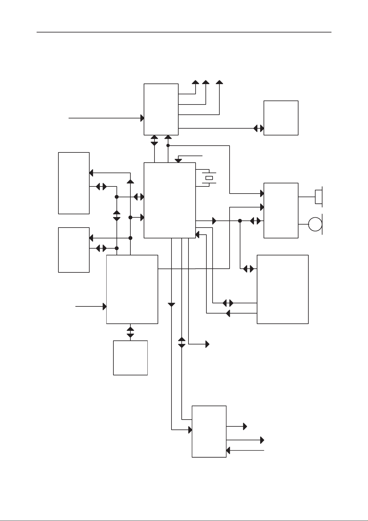
Interconnection Diagram of Baseband
VL VSL VA
PSCLD
N300
VBATT
SIM control
SBus
SIM
FLASH
8 Mbit
D430
control
Addr 19...0
data 7...0
D2BB2
ASIC
D400
13 MHz
32 kHz
Sync
Clock
SBus
System Module
SIM
READER
X300
AUDIO
CODEC
ST5090
N130
SRAM
1 Mbit
D440
Flash
loading
MBUS
H3001
MCU
D420
SBus
EEPROM
D446
TMS320C5
DSP
D360
DSPdata15...0
DSP addr 15...0
Synthe
Control
TxP
TxPwr
RxPwr
Original 34/96
RFI
N450
TxC
TxI,TxQ
RxI,RxQ
Page 4–39
Page 40
TFK–1
After Sales
System Module
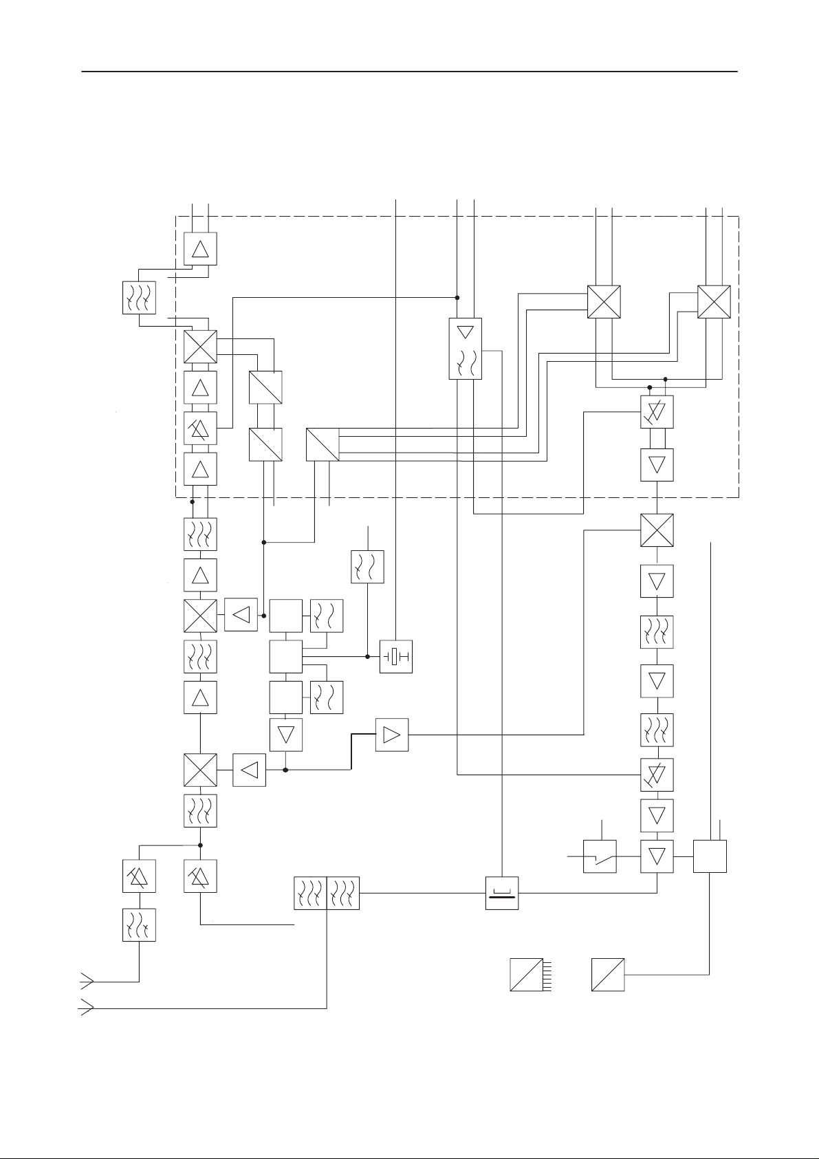
Block Diagram of RF
RXINN
RXINP
CRFRT
f/2
f
f/2
f
Technical Documentation
TXC
AFC
f/2
f
TXP
TX power control
TXIP
TXIN
TXQP
TXQN
VHF
UHF
PLL
VCO
VCO
sinewave
to ASIC
clipped sinewave
VCTCXO/
VCXO
Batt.volt.
TXC
TXP
+4V5_TX
BIAS
Page 4–40
+6 V
CRFCONT
+4.5V
+6 V
–4 V
Original 34/96
Page 41

After Sales
TFK–1
Technical Documentation
RF Frequency Plan
PCN
400
1805–
1880 313 87
LO 1
1710–
1785
1st IF 2nd IF
RX:
1492–1567
TX:
1510–1585
200
100
3rd IF
13
f/2
System Module
CRFRT
f
f
f/2
f
f/2
VCXO
13 MHz
LO 2
400
PLL
Original 34/96
Page 4–41
Page 42

TFK–1
After Sales
System Module
Power Distribution Diagram of RF
Battery
6 V
CRFCONT
Switch
Power
Amplifier
Technical Documentation
TXP
VXOPWR
PCN: 800 mA
RFIPWR
VR1 VR2 VR3 VR4 VR5 VR6 VR7 VR8Vbias
TX buffers
20 mA
VHLO:
VHF LO
30 mA
VCXO
2 mA
VPLL:+4V5_TX:
LMX2331
25 mA
+4V5_RX:
RF LNA
IF amps
PCN: 31 mA
V_prot
RFI:
Analog blocks
VTX:
CRFRT (VTX)
CRFRT (VTX_slow)
39 mA
VRX:
CRFRT (VRX)
35 mA
SYNTHPWR
TXPWR
RXPWR
15 mA
Page 4–42
Figure 1. Power distribution diagram
CRFRT (VB_ext)
< 1 mA
Original 34/96
RFREF
RFI
Page 43

After Sales
TFK–1
Technical Documentation
Block Diagram of Baseband
System Module
Original 34/96
Page 4–43
Page 44

TFK–1
After Sales
System Module
Circuit Diagram of Connectors
Technical Documentation
Page 4–44
Original 34/96
Page 45

After Sales
TFK–1
Technical Documentation
System Module
Circuit Diagram of Line Adapter Power Supply Unit
Original 34/96
Page 4–45
Page 46

TFK–1
After Sales
System Module
Circuit Diagram of 2 to 4 Wire Interface
Technical Documentation
Page 4–46
Original 34/96
Page 47

After Sales
TFK–1
Technical Documentation
Circuit Diagram of MCU Memory Block
System Module
Original 34/96
Page 4–47
Page 48

TFK–1
After Sales
System Module
Circuit Diagram of Power Supply
Technical Documentation
Page 4–48
Original 34/96
Page 49

After Sales
TFK–1
Technical Documentation
Circuit Diagram of Audio
System Module
Original 34/96
Page 4–49
Page 50

TFK–1
After Sales
System Module
Circuit Diagram of ASIC
Technical Documentation
Page 4–50
Original 34/96
Page 51

After Sales
TFK–1
Technical Documentation
Circuit Diagram of DSP Memory Block
System Module
Original 34/96
Page 4–51
Page 52

TFK–1
After Sales
System Module
Circuit Diagram of RFI
Technical Documentation
Page 4–52
Original 34/96
Page 53

After Sales
TFK–1
Technical Documentation
Circuit Diagram of Receiver
System Module
Original 34/96
Page 4–53
Page 54

TFK–1
After Sales
System Module
Circuit Diagram of Transceiver
Technical Documentation
Page 4–54
Original 34/96
Page 55

After Sales
TFK–1
Technical Documentation
Layout Diagrams of WT3
System Module
Original 34/96
Page 4–55
Page 56

TFK–1
After Sales
System Module
Technical Documentation
Parts list of WT3 (EDMS Issue 2.8) Code: 0200781
ITEM CODE DESCRIPTION VALUE TYPE
R100 1430035 Chip resistor 1.0 k 5 % 0.063 W 0603
R101 1430111 Chip resistor 1.0 M 5 % 0.063 W 0603
R102 1430111 Chip resistor 1.0 M 5 % 0.063 W 0603
R103 1430111 Chip resistor 1.0 M 5 % 0.063 W 0603
R104 1430111 Chip resistor 1.0 M 5 % 0.063 W 0603
R105 1430111 Chip resistor 1.0 M 5 % 0.063 W 0603
R106 1430111 Chip resistor 1.0 M 5 % 0.063 W 0603
R107 1430111 Chip resistor 1.0 M 5 % 0.063 W 0603
R108 1430111 Chip resistor 1.0 M 5 % 0.063 W 0603
R110 1430035 Chip resistor 1.0 k 5 % 0.063 W 0603
R111 1430065 Chip resistor 10 k 5 % 0.063 W 0603
R112 1430167 Chip resistor 47 5 % 0.063 W 0603
R113 1430051 Chip resistor 4.7 k 5 % 0.063 W 0603
R114 1430167 Chip resistor 47 5 % 0.063 W 0603
R115 1430065 Chip resistor 10 k 5 % 0.063 W 0603
R123 1430167 Chip resistor 47 5 % 0.063 W 0603
R124 1430167 Chip resistor 47 5 % 0.063 W 0603
R125 1430167 Chip resistor 47 5 % 0.063 W 0603
R126 1430051 Chip resistor 4.7 k 5 % 0.063 W 0603
R127 1430065 Chip resistor 10 k 5 % 0.063 W 0603
R128 1430001 Chip resistor 100 5 % 0.063 W 0603
R129 1430087 Chip resistor 100 k 5 % 0.063 W 0603
R131 1430087 Chip resistor 100 k 5 % 0.063 W 0603
R132 1430071 Chip resistor 22 k 5 % 0.063 W 0603
R133 1430087 Chip resistor 100 k 5 % 0.063 W 0603
R134 1430043 Chip resistor 2.2 k 5 % 0.063 W 0603
R135 1430065 Chip resistor 10 k 5 % 0.063 W 0603
R136 1430087 Chip resistor 100 k 5 % 0.063 W 0603
R137 1430087 Chip resistor 100 k 5 % 0.063 W 0603
R138 1430009 Chip resistor 220 5 % 0.063 W 0603
R141 1430043 Chip resistor 2.2 k 5 % 0.063 W 0603
R142 1430043 Chip resistor 2.2 k 5 % 0.063 W 0603
R143 1430087 Chip resistor 100 k 5 % 0.063 W 0603
R144 1430111 Chip resistor 1.0 M 5 % 0.063 W 0603
R145 1430111 Chip resistor 1.0 M 5 % 0.063 W 0603
R146 1430159 Chip resistor 22 5 % 0.063 W 0603
R147 1430159 Chip resistor 22 5 % 0.063 W 0603
R148 1430051 Chip resistor 4.7 k 5 % 0.063 W 0603
R149 1430065 Chip resistor 10 k 5 % 0.063 W 0603
R151 1430071 Chip resistor 22 k 5 % 0.063 W 0603
R152 1430071 Chip resistor 22 k 5 % 0.063 W 0603
R153 1430071 Chip resistor 22 k 5 % 0.063 W 0603
R154 1430071 Chip resistor 22 k 5 % 0.063 W 0603
Page 4–56
Original 34/96
Page 57

After Sales
TFK–1
Technical Documentation
R155 1430065 Chip resistor 10 k 5 % 0.063 W 0603
R156 1430051 Chip resistor 4.7 k 5 % 0.063 W 0603
R157 1430051 Chip resistor 4.7 k 5 % 0.063 W 0603
R163 1430087 Chip resistor 100 k 5 % 0.063 W 0603
R164 1430087 Chip resistor 100 k 5 % 0.063 W 0603
R165 1430087 Chip resistor 100 k 5 % 0.063 W 0603
R168 1430065 Chip resistor 10 k 5 % 0.063 W 0603
R169 1430095 Chip resistor 220 k 5 % 0.063 W 0603
R170 1430065 Chip resistor 10 k 5 % 0.063 W 0603
R172 1430071 Chip resistor 22 k 5 % 0.063 W 0603
R182 1430087 Chip resistor 100 k 5 % 0.063 W 0603
R183 1430087 Chip resistor 100 k 5 % 0.063 W 0603
R184 1430087 Chip resistor 100 k 5 % 0.063 W 0603
R185 1430087 Chip resistor 100 k 5 % 0.063 W 0603
R186 1430087 Chip resistor 100 k 5 % 0.063 W 0603
R190 1430111 Chip resistor 1.0 M 5 % 0.063 W 0603
R191 1430111 Chip resistor 1.0 M 5 % 0.063 W 0603
R201 1430159 Chip resistor 22 5 % 0.063 W 0603
R202 1430159 Chip resistor 22 5 % 0.063 W 0603
R203 1430087 Chip resistor 100 k 5 % 0.063 W 0603
R204 1430087 Chip resistor 100 k 5 % 0.063 W 0603
R205 1430099 Chip resistor 330 k 5 % 0.063 W 0603
R206 1430099 Chip resistor 330 k 5 % 0.063 W 0603
R207 1430085 Chip resistor 82 k 5 % 0.063 W 0603
R208 1430085 Chip resistor 82 k 5 % 0.063 W 0603
R209 1430085 Chip resistor 82 k 5 % 0.063 W 0603
R210 1430085 Chip resistor 82 k 5 % 0.063 W 0603
R211 1430159 Chip resistor 22 5 % 0.063 W 0603
R212 1430159 Chip resistor 22 5 % 0.063 W 0603
R213 1430087 Chip resistor 100 k 5 % 0.063 W 0603
R214 1430087 Chip resistor 100 k 5 % 0.063 W 0603
R215 1430099 Chip resistor 330 k 5 % 0.063 W 0603
R216 1430099 Chip resistor 330 k 5 % 0.063 W 0603
R217 1430099 Chip resistor 330 k 5 % 0.063 W 0603
R219 1430099 Chip resistor 330 k 5 % 0.063 W 0603
R221 1430087 Chip resistor 100 k 5 % 0.063 W 0603
R222 1430087 Chip resistor 100 k 5 % 0.063 W 0603
R223 1430065 Chip resistor 10 k 5 % 0.063 W 0603
R224 1430087 Chip resistor 100 k 5 % 0.063 W 0603
R225 1430087 Chip resistor 100 k 5 % 0.063 W 0603
R226 1430087 Chip resistor 100 k 5 % 0.063 W 0603
R227 1430065 Chip resistor 10 k 5 % 0.063 W 0603
R228 1430087 Chip resistor 100 k 5 % 0.063 W 0603
R231 1430111 Chip resistor 1.0 M 5 % 0.063 W 0603
R232 1430111 Chip resistor 1.0 M 5 % 0.063 W 0603
R233 1430111 Chip resistor 1.0 M 5 % 0.063 W 0603
R234 1430111 Chip resistor 1.0 M 5 % 0.063 W 0603
R240 1430111 Chip resistor 1.0 M 5 % 0.063 W 0603
System Module
Original 34/96
Page 4–57
Page 58

TFK–1
After Sales
System Module
R241 1430111 Chip resistor 1.0 M 5 % 0.063 W 0603
R250 1430043 Chip resistor 2.2 k 5 % 0.063 W 0603
R251 1430099 Chip resistor 330 k 5 % 0.063 W 0603
R252 1430065 Chip resistor 10 k 5 % 0.063 W 0603
R253 1430087 Chip resistor 100 k 5 % 0.063 W 0603
R254 1430111 Chip resistor 1.0 M 5 % 0.063 W 0603
R255 1430111 Chip resistor 1.0 M 5 % 0.063 W 0603
R256 1430071 Chip resistor 22 k 5 % 0.063 W 0603
R257 1430035 Chip resistor 1.0 k 5 % 0.063 W 0603
R260 1430085 Chip resistor 82 k 5 % 0.063 W 0603
R261 1430095 Chip resistor 220 k 5 % 0.063 W 0603
R262 1430085 Chip resistor 82 k 5 % 0.063 W 0603
R263 1430095 Chip resistor 220 k 5 % 0.063 W 0603
R264 1430079 Chip resistor 47 k 5 % 0.063 W 0603
R265 1430079 Chip resistor 47 k 5 % 0.063 W 0603
R266 1430065 Chip resistor 10 k 5 % 0.063 W 0603
R267 1430079 Chip resistor 47 k 5 % 0.063 W 0603
R268 1430111 Chip resistor 1.0 M 5 % 0.063 W 0603
R269 1430111 Chip resistor 1.0 M 5 % 0.063 W 0603
R270 1430087 Chip resistor 100 k 5 % 0.063 W 0603
R271 1430087 Chip resistor 100 k 5 % 0.063 W 0603
R272 1430099 Chip resistor 330 k 5 % 0.063 W 0603
R273 1430071 Chip resistor 22 k 5 % 0.063 W 0603
R274 1430065 Chip resistor 10 k 5 % 0.063 W 0603
R300 1430087 Chip resistor 100 k 5 % 0.063 W 0603
R301 1430087 Chip resistor 100 k 5 % 0.063 W 0603
R302 1430053 Chip resistor 5.6 k 5 % 0.063 W 0603
R311 1430035 Chip resistor 1.0 k 5 % 0.063 W 0603
R312 1430035 Chip resistor 1.0 k 5 % 0.063 W 0603
R313 1430035 Chip resistor 1.0 k 5 % 0.063 W 0603
R331 1430001 Chip resistor 100 5 % 0.063 W 0603
R332 1430001 Chip resistor 100 5 % 0.063 W 0603
R341 1430071 Chip resistor 22 k 5 % 0.063 W 0603
R342 1430039 Chip resistor 1.5 k 5 % 0.063 W 0603
R343 1430081 Chip resistor 56 k 5 % 0.063 W 0603
R344 1430065 Chip resistor 10 k 5 % 0.063 W 0603
R345 1430071 Chip resistor 22 k 5 % 0.063 W 0603
R361 1430167 Chip resistor 47 5 % 0.063 W 0603
R362 1430065 Chip resistor 10 k 5 % 0.063 W 0603
R371 1430015 Chip resistor 470 5 % 0.063 W 0603
R381 1430043 Chip resistor 2.2 k 5 % 0.063 W 0603
R382 1430043 Chip resistor 2.2 k 5 % 0.063 W 0603
R383 1430001 Chip resistor 100 5 % 0.063 W 0603
R384 1430043 Chip resistor 2.2 k 5 % 0.063 W 0603
R392 1430065 Chip resistor 10 k 5 % 0.063 W 0603
R400 1430013 Chip resistor 330 5 % 0.063 W 0603
R403 1430087 Chip resistor 100 k 5 % 0.063 W 0603
R407 1430087 Chip resistor 100 k 5 % 0.063 W 0603
Technical Documentation
Page 4–58
Original 34/96
Page 59

After Sales
TFK–1
Technical Documentation
R408 1430087 Chip resistor 100 k 5 % 0.063 W 0603
R409 1430087 Chip resistor 100 k 5 % 0.063 W 0603
R410 1430065 Chip resistor 10 k 5 % 0.063 W 0603
R411 1430065 Chip resistor 10 k 5 % 0.063 W 0603
R420 1430065 Chip resistor 10 k 5 % 0.063 W 0603
R421 1430035 Chip resistor 1.0 k 5 % 0.063 W 0603
R436 1430087 Chip resistor 100 k 5 % 0.063 W 0603
R437 1430167 Chip resistor 47 5 % 0.063 W 0603
R439 1430087 Chip resistor 100 k 5 % 0.063 W 0603
R440 1430065 Chip resistor 10 k 5 % 0.063 W 0603
R441 1430087 Chip resistor 100 k 5 % 0.063 W 0603
R442 1430065 Chip resistor 10 k 5 % 0.063 W 0603
R444 1430015 Chip resistor 470 5 % 0.063 W 0603
R445 1430015 Chip resistor 470 5 % 0.063 W 0603
R446 1430015 Chip resistor 470 5 % 0.063 W 0603
R447 1430015 Chip resistor 470 5 % 0.063 W 0603
R448 1430065 Chip resistor 10 k 5 % 0.063 W 0603
R449 1430065 Chip resistor 10 k 5 % 0.063 W 0603
R451 1430035 Chip resistor 1.0 k 5 % 0.063 W 0603
R452 1430035 Chip resistor 1.0 k 5 % 0.063 W 0603
R453 1430021 Chip resistor 680 5 % 0.063 W 0603
R454 1430021 Chip resistor 680 5 % 0.063 W 0603
R455 1430065 Chip resistor 10 k 5 % 0.063 W 0603
R456 1430079 Chip resistor 47 k 5 % 0.063 W 0603
R457 1800659 NTC resistor 47 k 10 % 0.12 W 0805
R460 1430065 Chip resistor 10 k 5 % 0.063 W 0603
R461 1430065 Chip resistor 10 k 5 % 0.063 W 0603
R501 1430151 Chip resistor 10 5 % 0.063 W 0603
R502 1430047 Chip resistor 3.3 k 5 % 0.063 W 0603
R503 1430047 Chip resistor 3.3 k 5 % 0.063 W 0603
R504 1430001 Chip resistor 100 5 % 0.063 W 0603
R505 1430055 Chip resistor 6.8 k 5 % 0.063 W 0603
R506 1430035 Chip resistor 1.0 k 5 % 0.063 W 0603
R507 1430035 Chip resistor 1.0 k 5 % 0.063 W 0603
R508 1430035 Chip resistor 1.0 k 5 % 0.063 W 0603
R509 1430001 Chip resistor 100 5 % 0.063 W 0603
R511 1430087 Chip resistor 100 k 5 % 0.063 W 0603
R512 1430087 Chip resistor 100 k 5 % 0.063 W 0603
R513 1430087 Chip resistor 100 k 5 % 0.063 W 0603
R514 1430087 Chip resistor 100 k 5 % 0.063 W 0603
R515 1430055 Chip resistor 6.8 k 5 % 0.063 W 0603
R518 1430035 Chip resistor 1.0 k 5 % 0.063 W 0603
R519 1430035 Chip resistor 1.0 k 5 % 0.063 W 0603
R521 1430015 Chip resistor 470 5 % 0.063 W 0603
R522 1430041 Chip resistor 1.8 k 5 % 0.063 W 0603
R523 1430037 Chip resistor 1.2 k 5 % 0.063 W 0603
R524 1430009 Chip resistor 220 5 % 0.063 W 0603
R525 1430159 Chip resistor 22 5 % 0.063 W 0603
System Module
Original 34/96
Page 4–59
Page 60

TFK–1
After Sales
System Module
R526 1430051 Chip resistor 4.7 k 5 % 0.063 W 0603
R527 1430065 Chip resistor 10 k 5 % 0.063 W 0603
R528 1430007 Chip resistor 180 5 % 0.063 W 0603
R529 1430159 Chip resistor 22 5 % 0.063 W 0603
R531 1430159 Chip resistor 22 5 % 0.063 W 0603
R532 1430171 Chip resistor 68 5 % 0.063 W 0603
R533 1430039 Chip resistor 1.5 k 5 % 0.063 W 0603
R534 1430055 Chip resistor 6.8 k 5 % 0.063 W 0603
R535 1430159 Chip resistor 22 5 % 0.063 W 0603
R541 1430159 Chip resistor 22 5 % 0.063 W 0603
R543 1430013 Chip resistor 330 5 % 0.063 W 0603
R544 1430043 Chip resistor 2.2 k 5 % 0.063 W 0603
R545 1430039 Chip resistor 1.5 k 5 % 0.063 W 0603
R546 1430171 Chip resistor 68 5 % 0.063 W 0603
R547 1430015 Chip resistor 470 5 % 0.063 W 0603
R548 1430013 Chip resistor 330 5 % 0.063 W 0603
R549 1430065 Chip resistor 10 k 5 % 0.063 W 0603
R550 1430065 Chip resistor 10 k 5 % 0.063 W 0603
R551 1430053 Chip resistor 5.6 k 5 % 0.063 W 0603
R552 1430065 Chip resistor 10 k 5 % 0.063 W 0603
R553 1430053 Chip resistor 5.6 k 5 % 0.063 W 0603
R554 1430053 Chip resistor 5.6 k 5 % 0.063 W 0603
R555 1430065 Chip resistor 10 k 5 % 0.063 W 0603
R556 1430053 Chip resistor 5.6 k 5 % 0.063 W 0603
R557 1430005 Chip resistor 150 5 % 0.063 W 0603
R558 1430007 Chip resistor 180 5 % 0.063 W 0603
R559 1430013 Chip resistor 330 5 % 0.063 W 0603
R560 1430047 Chip resistor 3.3 k 5 % 0.063 W 0603
R561 1430073 Chip resistor 27 k 5 % 0.063 W 0603
R562 1430035 Chip resistor 1.0 k 5 % 0.063 W 0603
R563 1430001 Chip resistor 100 5 % 0.063 W 0603
R566 1430035 Chip resistor 1.0 k 5 % 0.063 W 0603
R568 1430001 Chip resistor 100 5 % 0.063 W 0603
R570 1430001 Chip resistor 100 5 % 0.063 W 0603
R571 1430043 Chip resistor 2.2 k 5 % 0.063 W 0603
R572 1430079 Chip resistor 47 k 5 % 0.063 W 0603
R573 1430065 Chip resistor 10 k 5 % 0.063 W 0603
R574 1430071 Chip resistor 22 k 5 % 0.063 W 0603
R576 1430035 Chip resistor 1.0 k 5 % 0.063 W 0603
R578 1430077 Chip resistor 39 k 5 % 0.063 W 0603
R579 1430065 Chip resistor 10 k 5 % 0.063 W 0603
R580 1430073 Chip resistor 27 k 5 % 0.063 W 0603
R601 1430043 Chip resistor 2.2 k 5 % 0.063 W 0603
R602 1430043 Chip resistor 2.2 k 5 % 0.063 W 0603
R603 1430043 Chip resistor 2.2 k 5 % 0.063 W 0603
R701 1430051 Chip resistor 4.7 k 5 % 0.063 W 0603
R703 1430043 Chip resistor 2.2 k 5 % 0.063 W 0603
R704 1430159 Chip resistor 22 5 % 0.063 W 0603
Technical Documentation
Page 4–60
Original 34/96
Page 61

After Sales
TFK–1
Technical Documentation
R705 1430007 Chip resistor 180 5 % 0.063 W 0603
R710 1430144 Chip jumper 0603
R719 1430144 Chip jumper 0603
R721 1430151 Chip resistor 10 5 % 0.063 W 0603
R722 1430013 Chip resistor 330 5 % 0.063 W 0603
R723 1430045 Chip resistor 2.7 k 5 % 0.063 W 0603
R724 1430001 Chip resistor 100 5 % 0.063 W 0603
R725 1430039 Chip resistor 1.5 k 5 % 0.063 W 0603
R731 1430073 Chip resistor 27 k 5 % 0.063 W 0603
R732 1430007 Chip resistor 180 5 % 0.063 W 0603
R733 1430069 Chip resistor 18 k 5 % 0.063 W 0603
R734 1430043 Chip resistor 2.2 k 5 % 0.063 W 0603
R735 1430001 Chip resistor 100 5 % 0.063 W 0603
R736 1430159 Chip resistor 22 5 % 0.063 W 0603
R737 1430009 Chip resistor 220 5 % 0.063 W 0603
R738 1430009 Chip resistor 220 5 % 0.063 W 0603
R741 1430037 Chip resistor 1.2 k 5 % 0.063 W 0603
R742 1430159 Chip resistor 22 5 % 0.063 W 0603
R743 1430043 Chip resistor 2.2 k 5 % 0.063 W 0603
R744 1430043 Chip resistor 2.2 k 5 % 0.063 W 0603
R745 1430013 Chip resistor 330 5 % 0.063 W 0603
R746 1430035 Chip resistor 1.0 k 5 % 0.063 W 0603
R751 1412279 Chip resistor 2.2 5 % 0.1 W 0805
R752 1430035 Chip resistor 1.0 k 5 % 0.063 W 0603
R753 1430043 Chip resistor 2.2 k 5 % 0.063 W 0603
R761 1420200 Chip resistor 0.22 5 % 0.2 W 1206
R762 1430005 Chip resistor 150 5 % 0.063 W 0603
R763 1430013 Chip resistor 330 5 % 0.063 W 0603
R764 1430035 Chip resistor 1.0 k 5 % 0.063 W 0603
R765 1430043 Chip resistor 2.2 k 5 % 0.063 W 0603
R771 1430047 Chip resistor 3.3 k 5 % 0.063 W 0603
R772 1430055 Chip resistor 6.8 k 5 % 0.063 W 0603
R773 1430055 Chip resistor 6.8 k 5 % 0.063 W 0603
R774 1430071 Chip resistor 22 k 5 % 0.063 W 0603
R775 1430035 Chip resistor 1.0 k 5 % 0.063 W 0603
R776 1430065 Chip resistor 10 k 5 % 0.063 W 0603
R777 1430037 Chip resistor 1.2 k 5 % 0.063 W 0603
R778 1430043 Chip resistor 2.2 k 5 % 0.063 W 0603
R779 1430043 Chip resistor 2.2 k 5 % 0.063 W 0603
R780 1430065 Chip resistor 10 k 5 % 0.063 W 0603
R781 1430043 Chip resistor 2.2 k 5 % 0.063 W 0603
R783 1430043 Chip resistor 2.2 k 5 % 0.063 W 0603
R784 1430167 Chip resistor 47 5 % 0.063 W 0603
R785 1430007 Chip resistor 180 5 % 0.063 W 0603
R786 1430041 Chip resistor 1.8 k 5 % 0.063 W 0603
R790 1430069 Chip resistor 18 k 5 % 0.063 W 0603
R791 1430167 Chip resistor 47 5 % 0.063 W 0603
R793 1430051 Chip resistor 4.7 k 5 % 0.063 W 0603
System Module
Original 34/96
Page 4–61
Page 62

TFK–1
After Sales
System Module
R794 1430001 Chip resistor 100 5 % 0.063 W 0603
R800 1430065 Chip resistor 10 k 5 % 0.063 W 0603
R801 1430079 Chip resistor 47 k 5 % 0.063 W 0603
R802 1430079 Chip resistor 47 k 5 % 0.063 W 0603
R803 1430001 Chip resistor 100 5 % 0.063 W 0603
R804 1430069 Chip resistor 18 k 5 % 0.063 W 0603
R805 1430069 Chip resistor 18 k 5 % 0.063 W 0603
R806 1430065 Chip resistor 10 k 5 % 0.063 W 0603
R807 1430041 Chip resistor 1.8 k 5 % 0.063 W 0603
R808 1430035 Chip resistor 1.0 k 5 % 0.063 W 0603
R809 1430071 Chip resistor 22 k 5 % 0.063 W 0603
R810 1430035 Chip resistor 1.0 k 5 % 0.063 W 0603
R811 1430051 Chip resistor 4.7 k 5 % 0.063 W 0603
R812 1430051 Chip resistor 4.7 k 5 % 0.063 W 0603
R813 1430051 Chip resistor 4.7 k 5 % 0.063 W 0603
R814 1430065 Chip resistor 10 k 5 % 0.063 W 0603
R815 1430069 Chip resistor 18 k 5 % 0.063 W 0603
R816 1430065 Chip resistor 10 k 5 % 0.063 W 0603
R817 1430001 Chip resistor 100 5 % 0.063 W 0603
R818 1430159 Chip resistor 22 5 % 0.063 W 0603
R819 1430159 Chip resistor 22 5 % 0.063 W 0603
R821 1430069 Chip resistor 18 k 5 % 0.063 W 0603
R822 1430049 Chip resistor 3.9 k 5 % 0.063 W 0603
R823 1430167 Chip resistor 47 5 % 0.063 W 0603
R824 1430001 Chip resistor 100 5 % 0.063 W 0603
R831 1430035 Chip resistor 1.0 k 5 % 0.063 W 0603
R832 1430035 Chip resistor 1.0 k 5 % 0.063 W 0603
R833 1430013 Chip resistor 330 5 % 0.063 W 0603
R834 1430001 Chip resistor 100 5 % 0.063 W 0603
R840 1430069 Chip resistor 18 k 5 % 0.063 W 0603
R841 1430051 Chip resistor 4.7 k 5 % 0.063 W 0603
R842 1430051 Chip resistor 4.7 k 5 % 0.063 W 0603
R843 1430045 Chip resistor 2.7 k 5 % 0.063 W 0603
R844 1430009 Chip resistor 220 5 % 0.063 W 0603
R845 1430151 Chip resistor 10 5 % 0.063 W 0603
R846 1430159 Chip resistor 22 5 % 0.063 W 0603
R847 1430167 Chip resistor 47 5 % 0.063 W 0603
R848 1430151 Chip resistor 10 5 % 0.063 W 0603
R849 1430035 Chip resistor 1.0 k 5 % 0.063 W 0603
R863 1430015 Chip resistor 470 5 % 0.063 W 0603
C101 2320059 Ceramic cap. 100 p 5 % 50 V 0603
C102 2320059 Ceramic cap. 100 p 5 % 50 V 0603
C103 2320059 Ceramic cap. 100 p 5 % 50 V 0603
C104 2320059 Ceramic cap. 100 p 5 % 50 V 0603
C105 2320059 Ceramic cap. 100 p 5 % 50 V 0603
C106 2320059 Ceramic cap. 100 p 5 % 50 V 0603
C107 2320059 Ceramic cap. 100 p 5 % 50 V 0603
C108 2320059 Ceramic cap. 100 p 5 % 50 V 0603
Technical Documentation
Page 4–62
Original 34/96
Page 63

After Sales
TFK–1
Technical Documentation
C110 2320083 Ceramic cap. 1.0 n 5 % 50 V 0603
C121 2320045 Ceramic cap. 27 p 5 % 50 V 0603
C122 2320045 Ceramic cap. 27 p 5 % 50 V 0603
C123 2320045 Ceramic cap. 27 p 5 % 50 V 0603
C124 2320045 Ceramic cap. 27 p 5 % 50 V 0603
C125 2320045 Ceramic cap. 27 p 5 % 50 V 0603
C126 2320045 Ceramic cap. 27 p 5 % 50 V 0603
C127 2320045 Ceramic cap. 27 p 5 % 50 V 0603
C128 2320045 Ceramic cap. 27 p 5 % 50 V 0603
C129 2310791 Ceramic cap. 33 n 20 % 50 V 0805
C130 2310791 Ceramic cap. 33 n 20 % 50 V 0805
C131 2611668 Tantalum cap. 4.7 u 20 % 10 V 3.2x1.6x1.6
C132 2312410 Ceramic cap. 1.0 u 10 % 16 V 1206
C133 2320107 Ceramic cap. 10 n 5 % 50 V 0603
C134 2320107 Ceramic cap. 10 n 5 % 50 V 0603
C135 2320107 Ceramic cap. 10 n 5 % 50 V 0603
C136 2320083 Ceramic cap. 1.0 n 5 % 50 V 0603
C137 2320107 Ceramic cap. 10 n 5 % 50 V 0603
C138 2320107 Ceramic cap. 10 n 5 % 50 V 0603
C139 2320083 Ceramic cap. 1.0 n 5 % 50 V 0603
C140 2320107 Ceramic cap. 10 n 5 % 50 V 0603
C141 2307816 Ceramic cap. 47 n 20 % 25 V 0805
C142 2604431 Tantalum cap. 10 u 20 % 16 V 6.0x3.2x2.5
C143 2320099 Ceramic cap. 4.7 n 5 % 50 V 0603
C144 2320099 Ceramic cap. 4.7 n 5 % 50 V 0603
C145 2604382 Tantalum cap. 6.8 u 20 % 35 V 7.3x4.4x2.8
C146 2604382 Tantalum cap. 6.8 u 20 % 35 V 7.3x4.4x2.8
C147 2320083 Ceramic cap. 1.0 n 5 % 50 V 0603
C148 2611668 Tantalum cap. 4.7 u 20 % 10 V 3.2x1.6x1.6
C149 2611668 Tantalum cap. 4.7 u 20 % 10 V 3.2x1.6x1.6
C151 2307816 Ceramic cap. 47 n 20 % 25 V 0805
C152 2320083 Ceramic cap. 1.0 n 5 % 50 V 0603
C153 2310784 Ceramic cap. 100 n 10 % 25 V 0805
C154 2310784 Ceramic cap. 100 n 10 % 25 V 0805
C181 2320107 Ceramic cap. 10 n 5 % 50 V 0603
C190 2604382 Tantalum cap. 6.8 u 20 % 35 V 7.3x4.4x2.8
C191 2604382 Tantalum cap. 6.8 u 20 % 35 V 7.3x4.4x2.8
C231 2310791 Ceramic cap. 33 n 20 % 50 V 0805
C232 2310791 Ceramic cap. 33 n 20 % 50 V 0805
C233 2310791 Ceramic cap. 33 n 20 % 50 V 0805
C234 2310791 Ceramic cap. 33 n 20 % 50 V 0805
C240 2604079 Tantalum cap. 0.22 u 20 % 35 V 3.2x1.6x1.6
C241 2604079 Tantalum cap. 0.22 u 20 % 35 V 3.2x1.6x1.6
C251 2307816 Ceramic cap. 47 n 20 % 25 V 0805
C252 2307816 Ceramic cap. 47 n 20 % 25 V 0805
C254 2310791 Ceramic cap. 33 n 20 % 50 V 0805
C255 2312410 Ceramic cap. 1.0 u 10 % 16 V 1206
C256 2312410 Ceramic cap. 1.0 u 10 % 16 V 1206
System Module
Original 34/96
Page 4–63
Page 64

TFK–1
After Sales
System Module
C257 2310791 Ceramic cap. 33 n 20 % 50 V 0805
C260 2312410 Ceramic cap. 1.0 u 10 % 16 V 1206
C261 2320059 Ceramic cap. 100 p 5 % 50 V 0603
C270 2320067 Ceramic cap. 220 p 5 % 50 V 0603
C271 2320059 Ceramic cap. 100 p 5 % 50 V 0603
C272 2320120 Ceramic cap. 22 n 10 % 25 V 0603
C301 2320107 Ceramic cap. 10 n 5 % 50 V 0603
C302 2604431 Tantalum cap. 10 u 20 % 16 V 6.0x3.2x2.5
C303 2320107 Ceramic cap. 10 n 5 % 50 V 0603
C311 2320107 Ceramic cap. 10 n 5 % 50 V 0603
C312 2320107 Ceramic cap. 10 n 5 % 50 V 0603
C313 2610153 Tantalum cap. 10 u 20 % 6.0x3.2x2.5
C314 2320107 Ceramic cap. 10 n 5 % 50 V 0603
C315 2320107 Ceramic cap. 10 n 5 % 50 V 0603
C316 2320107 Ceramic cap. 10 n 5 % 50 V 0603
C317 2312410 Ceramic cap. 1.0 u 10 % 16 V 1206
C318 2320083 Ceramic cap. 1.0 n 5 % 50 V 0603
C319 2610153 Tantalum cap. 10 u 20 % 6.0x3.2x2.5
C320 2320107 Ceramic cap. 10 n 5 % 50 V 0603
C321 2610153 Tantalum cap. 10 u 20 % 6.0x3.2x2.5
C322 2320107 Ceramic cap. 10 n 5 % 50 V 0603
C331 2312410 Ceramic cap. 1.0 u 10 % 16 V 1206
C332 2310784 Ceramic cap. 100 n 10 % 25 V 0805
C333 2320107 Ceramic cap. 10 n 5 % 50 V 0603
C334 2320043 Ceramic cap. 22 p 5 % 50 V 0603
C335 2320059 Ceramic cap. 100 p 5 % 50 V 0603
C336 2320043 Ceramic cap. 22 p 5 % 50 V 0603
C341 2320107 Ceramic cap. 10 n 5 % 50 V 0603
C342 2610153 Tantalum cap. 10 u 20 % 6.0x3.2x2.5
C351 2610153 Tantalum cap. 10 u 20 % 6.0x3.2x2.5
C352 2320107 Ceramic cap. 10 n 5 % 50 V 0603
C360 2310791 Ceramic cap. 33 n 20 % 50 V 0805
C361 2310791 Ceramic cap. 33 n 20 % 50 V 0805
C365 2320059 Ceramic cap. 100 p 5 % 50 V 0603
C366 2312410 Ceramic cap. 1.0 u 10 % 16 V 1206
C371 2310791 Ceramic cap. 33 n 20 % 50 V 0805
C372 2310791 Ceramic cap. 33 n 20 % 50 V 0805
C373 2310791 Ceramic cap. 33 n 20 % 50 V 0805
C381 2310791 Ceramic cap. 33 n 20 % 50 V 0805
C382 2310791 Ceramic cap. 33 n 20 % 50 V 0805
C383 2310791 Ceramic cap. 33 n 20 % 50 V 0805
C400 2310791 Ceramic cap. 33 n 20 % 50 V 0805
C401 2310791 Ceramic cap. 33 n 20 % 50 V 0805
C403 2320083 Ceramic cap. 1.0 n 5 % 50 V 0603
C404 2320053 Ceramic cap. 56 p 5 % 50 V 0603
C405 2320035 Ceramic cap. 10 p 5 % 50 V 0603
C406 2312410 Ceramic cap. 1.0 u 10 % 16 V 1206
C407 2320059 Ceramic cap. 100 p 5 % 50 V 0603
Technical Documentation
Page 4–64
Original 34/96
Page 65

After Sales
TFK–1
Technical Documentation
C408 2312410 Ceramic cap. 1.0 u 10 % 16 V 1206
C409 2320059 Ceramic cap. 100 p 5 % 50 V 0603
C410 2320059 Ceramic cap. 100 p 5 % 50 V 0603
C420 2310791 Ceramic cap. 33 n 20 % 50 V 0805
C421 2310791 Ceramic cap. 33 n 20 % 50 V 0805
C430 2310791 Ceramic cap. 33 n 20 % 50 V 0805
C431 2312410 Ceramic cap. 1.0 u 10 % 16 V 1206
C432 2320059 Ceramic cap. 100 p 5 % 50 V 0603
C433 2310791 Ceramic cap. 33 n 20 % 50 V 0805
C440 2310791 Ceramic cap. 33 n 20 % 50 V 0805
C441 2312410 Ceramic cap. 1.0 u 10 % 16 V 1206
C442 2320059 Ceramic cap. 100 p 5 % 50 V 0603
C445 2310791 Ceramic cap. 33 n 20 % 50 V 0805
C451 2320059 Ceramic cap. 100 p 5 % 50 V 0603
C452 2320059 Ceramic cap. 100 p 5 % 50 V 0603
C453 2310791 Ceramic cap. 33 n 20 % 50 V 0805
C454 2310791 Ceramic cap. 33 n 20 % 50 V 0805
C455 2312410 Ceramic cap. 1.0 u 10 % 16 V 1206
C456 2320110 Ceramic cap. 10 n 10 % 50 V 0603
C457 2312410 Ceramic cap. 1.0 u 10 % 16 V 1206
C458 2320110 Ceramic cap. 10 n 10 % 50 V 0603
C459 2312410 Ceramic cap. 1.0 u 10 % 16 V 1206
C460 2320059 Ceramic cap. 100 p 5 % 50 V 0603
C461 2312410 Ceramic cap. 1.0 u 10 % 16 V 1206
C462 2320110 Ceramic cap. 10 n 10 % 50 V 0603
C501 2320011 Ceramic cap. 1.0 p 0.25 % 50 V 0603
C502 2320095 Ceramic cap. 3.3 n 5 % 50 V 0603
C503 2320043 Ceramic cap. 22 p 5 % 50 V 0603
C504 2320083 Ceramic cap. 1.0 n 5 % 50 V 0603
C505 2320011 Ceramic cap. 1.0 p 0.25 % 50 V 0603
C506 2320027 Ceramic cap. 4.7 p 0.25 % 50 V 0603
C508 2320083 Ceramic cap. 1.0 n 5 % 50 V 0603
C509 2320027 Ceramic cap. 4.7 p 0.25 % 50 V 0603
C510 2320043 Ceramic cap. 22 p 5 % 50 V 0603
C511 2320039 Ceramic cap. 15 p 5 % 50 V 0603
C513 2320015 Ceramic cap. 1.5 p 0.25 % 50 V 0603
C514 2320043 Ceramic cap. 22 p 5 % 50 V 0603
C515 2320017 Ceramic cap. 1.8 p 0.25 % 50 V 0603
C516 2320027 Ceramic cap. 4.7 p 0.25 % 50 V 0603
C517 2320039 Ceramic cap. 15 p 5 % 50 V 0603
C518 2320095 Ceramic cap. 3.3 n 5 % 50 V 0603
C519 2320059 Ceramic cap. 100 p 5 % 50 V 0603
C520 2320013 Ceramic cap. 1.2 p 0.25 % 50 V 0603
C521 2320013 Ceramic cap. 1.2 p 0.25 % 50 V 0603
C522 2320033 Ceramic cap. 8.2 p 0.25 % 50 V 0603
C523 2320083 Ceramic cap. 1.0 n 5 % 50 V 0603
C524 2320059 Ceramic cap. 100 p 5 % 50 V 0603
C525 2320027 Ceramic cap. 4.7 p 0.25 % 50 V 0603
System Module
Original 34/96
Page 4–65
Page 66

TFK–1
After Sales
System Module
C526 2320043 Ceramic cap. 22 p 5 % 50 V 0603
C527 2320043 Ceramic cap. 22 p 5 % 50 V 0603
C528 2320043 Ceramic cap. 22 p 5 % 50 V 0603
C529 2320043 Ceramic cap. 22 p 5 % 50 V 0603
C530 2320019 Ceramic cap. 2.2 p 0.25 % 50 V 0603
C531 2320035 Ceramic cap. 10 p 5 % 50 V 0603
C532 2320011 Ceramic cap. 1.0 p 0.25 % 50 V 0603
C533 2320083 Ceramic cap. 1.0 n 5 % 50 V 0603
C534 2320095 Ceramic cap. 3.3 n 5 % 50 V 0603
C536 2320035 Ceramic cap. 10 p 5 % 50 V 0603
C537 2320029 Ceramic cap. 5.6 p 0.25 % 50 V 0603
C538 2320039 Ceramic cap. 15 p 5 % 50 V 0603
C539 2320049 Ceramic cap. 39 p 5 % 50 V 0603
C541 2320095 Ceramic cap. 3.3 n 5 % 50 V 0603
C542 2320083 Ceramic cap. 1.0 n 5 % 50 V 0603
C543 2320095 Ceramic cap. 3.3 n 5 % 50 V 0603
C544 2320083 Ceramic cap. 1.0 n 5 % 50 V 0603
C545 2320059 Ceramic cap. 100 p 5 % 50 V 0603
C546 2320059 Ceramic cap. 100 p 5 % 50 V 0603
C547 2320043 Ceramic cap. 22 p 5 % 50 V 0603
C548 2320031 Ceramic cap. 6.8 p 0.25 % 50 V 0603
C551 2320033 Ceramic cap. 8.2 p 0.25 % 50 V 0603
C552 2320059 Ceramic cap. 100 p 5 % 50 V 0603
C553 2320059 Ceramic cap. 100 p 5 % 50 V 0603
C554 2320063 Ceramic cap. 150 p 5 % 50 V 0603
C555 2320063 Ceramic cap. 150 p 5 % 50 V 0603
C556 2320091 Ceramic cap. 2.2 n 5 % 50 V 0603
C557 2320059 Ceramic cap. 100 p 5 % 50 V 0603
C558 2320059 Ceramic cap. 100 p 5 % 50 V 0603
C559 2320091 Ceramic cap. 2.2 n 5 % 50 V 0603
C560 2320091 Ceramic cap. 2.2 n 5 % 50 V 0603
C561 2320059 Ceramic cap. 100 p 5 % 50 V 0603
C562 2320075 Ceramic cap. 470 p 5 % 50 V 0603
C563 2320053 Ceramic cap. 56 p 5 % 50 V 0603
C566 2320053 Ceramic cap. 56 p 5 % 50 V 0603
C569 2320095 Ceramic cap. 3.3 n 5 % 50 V 0603
C570 2320131 Ceramic cap. 33 n 10 % 16 V 0603
C571 2320095 Ceramic cap. 3.3 n 5 % 50 V 0603
C572 2310791 Ceramic cap. 33 n 20 % 50 V 0805
C573 2320053 Ceramic cap. 56 p 5 % 50 V 0603
C574 2320053 Ceramic cap. 56 p 5 % 50 V 0603
C575 2320029 Ceramic cap. 5.6 p 0.25 % 50 V 0603
C580 2320083 Ceramic cap. 1.0 n 5 % 50 V 0603
C600 2312410 Ceramic cap. 1.0 u 10 % 16 V 1206
C601 2310784 Ceramic cap. 100 n 10 % 25 V 0805
C602 2312410 Ceramic cap. 1.0 u 10 % 16 V 1206
C603 2312410 Ceramic cap. 1.0 u 10 % 16 V 1206
C604 2310784 Ceramic cap. 100 n 10 % 25 V 0805
Technical Documentation
Page 4–66
Original 34/96
Page 67

After Sales
TFK–1
Technical Documentation
C606 2310784 Ceramic cap. 100 n 10 % 25 V 0805
C607 2312410 Ceramic cap. 1.0 u 10 % 16 V 1206
C608 2312410 Ceramic cap. 1.0 u 10 % 16 V 1206
C609 2310784 Ceramic cap. 100 n 10 % 25 V 0805
C610 2310784 Ceramic cap. 100 n 10 % 25 V 0805
C701 2320047 Ceramic cap. 33 p 5 % 50 V 0603
C702 2320023 Ceramic cap. 3.3 p 0.25 % 50 V 0603
C703 2320095 Ceramic cap. 3.3 n 5 % 50 V 0603
C704 2320059 Ceramic cap. 100 p 5 % 50 V 0603
C705 2320015 Ceramic cap. 1.5 p 0.25 % 50 V 0603
C706 2320013 Ceramic cap. 1.2 p 0.25 % 50 V 0603
C710 2320083 Ceramic cap. 1.0 n 5 % 50 V 0603
C711 2320035 Ceramic cap. 10 p 5 % 50 V 0603
C714 2320023 Ceramic cap. 3.3 p 0.25 % 50 V 0603
C715 2320019 Ceramic cap. 2.2 p 0.25 % 50 V 0603
C716 2320021 Ceramic cap. 2.7 p 0.25 % 50 V 0603
C721 2320083 Ceramic cap. 1.0 n 5 % 50 V 0603
C722 2320035 Ceramic cap. 10 p 5 % 50 V 0603
C723 2320023 Ceramic cap. 3.3 p 0.25 % 50 V 0603
C724 2320027 Ceramic cap. 4.7 p 0.25 % 50 V 0603
C725 2320011 Ceramic cap. 1.0 p 0.25 % 50 V 0603
C726 2320017 Ceramic cap. 1.8 p 0.25 % 50 V 0603
C731 2320029 Ceramic cap. 5.6 p 0.25 % 50 V 0603
C732 2320059 Ceramic cap. 100 p 5 % 50 V 0603
C733 2320023 Ceramic cap. 3.3 p 0.25 % 50 V 0603
C736 2320015 Ceramic cap. 1.5 p 0.25 % 50 V 0603
C737 2320027 Ceramic cap. 4.7 p 0.25 % 50 V 0603
C738 2320017 Ceramic cap. 1.8 p 0.25 % 50 V 0603
C741 2320059 Ceramic cap. 100 p 5 % 50 V 0603
C742 2320083 Ceramic cap. 1.0 n 5 % 50 V 0603
C743 2320043 Ceramic cap. 22 p 5 % 50 V 0603
C744 2320059 Ceramic cap. 100 p 5 % 50 V 0603
C745 2320017 Ceramic cap. 1.8 p 0.25 % 50 V 0603
C746 2320017 Ceramic cap. 1.8 p 0.25 % 50 V 0603
C751 2320083 Ceramic cap. 1.0 n 5 % 50 V 0603
C752 2320083 Ceramic cap. 1.0 n 5 % 50 V 0603
C753 2320043 Ceramic cap. 22 p 5 % 50 V 0603
C754 2320021 Ceramic cap. 2.7 p 0.25 % 50 V 0603
C755 2320059 Ceramic cap. 100 p 5 % 50 V 0603
C756 2320021 Ceramic cap. 2.7 p 0.25 % 50 V 0603
C757 2320083 Ceramic cap. 1.0 n 5 % 50 V 0603
C760 2320083 Ceramic cap. 1.0 n 5 % 50 V 0603
C761 2320053 Ceramic cap. 56 p 5 % 50 V 0603
C762 2320043 Ceramic cap. 22 p 5 % 50 V 0603
C763 2320029 Ceramic cap. 5.6 p 0.25 % 50 V 0603
C764 2320075 Ceramic cap. 470 p 5 % 50 V 0603
C765 2320023 Ceramic cap. 3.3 p 0.25 % 50 V 0603
C766 2320013 Ceramic cap. 1.2 p 0.25 % 50 V 0603
System Module
Original 34/96
Page 4–67
Page 68

TFK–1
After Sales
System Module
C767 2320013 Ceramic cap. 1.2 p 0.25 % 50 V 0603
C768 2320083 Ceramic cap. 1.0 n 5 % 50 V 0603
C770 2500708 Electrol. cap. 3300 u 20 % 16 V
C781 2320045 Ceramic cap. 27 p 5 % 50 V 0603
C782 2320095 Ceramic cap. 3.3 n 5 % 50 V 0603
C783 2320043 Ceramic cap. 22 p 5 % 50 V 0603
C784 2320035 Ceramic cap. 10 p 5 % 50 V 0603
C785 2320035 Ceramic cap. 10 p 5 % 50 V 0603
C791 2610200 Tantalum cap. 2.2 u 20 % 2.0x1.3x1.2
C792 2610200 Tantalum cap. 2.2 u 20 % 2.0x1.3x1.2
C793 2610200 Tantalum cap. 2.2 u 20 % 2.0x1.3x1.2
C794 2611668 Tantalum cap. 4.7 u 20 % 10 V 3.2x1.6x1.6
C796 2610100 Tantalum cap. 1 u 20 % 10 V 2.0x1.3x1.2
C800 2604079 Tantalum cap. 0.22 u 20 % 35 V 3.2x1.6x1.6
C801 2310791 Ceramic cap. 33 n 20 % 50 V 0805
C803 2320067 Ceramic cap. 220 p 5 % 50 V 0603
C804 2320047 Ceramic cap. 33 p 5 % 50 V 0603
C805 2320067 Ceramic cap. 220 p 5 % 50 V 0603
C806 2610100 Tantalum cap. 1 u 20 % 10 V 2.0x1.3x1.2
C807 2320095 Ceramic cap. 3.3 n 5 % 50 V 0603
C808 2320019 Ceramic cap. 2.2 p 0.25 % 50 V 0603
C809 2320083 Ceramic cap. 1.0 n 5 % 50 V 0603
C811 2320027 Ceramic cap. 4.7 p 0.25 % 50 V 0603
C812 2320027 Ceramic cap. 4.7 p 0.25 % 50 V 0603
C813 2320027 Ceramic cap. 4.7 p 0.25 % 50 V 0603
C814 2320011 Ceramic cap. 1.0 p 0.25 % 50 V 0603
C815 2320099 Ceramic cap. 4.7 n 5 % 50 V 0603
C816 2320059 Ceramic cap. 100 p 5 % 50 V 0603
C817 2320059 Ceramic cap. 100 p 5 % 50 V 0603
C818 2320067 Ceramic cap. 220 p 5 % 50 V 0603
C819 2610100 Tantalum cap. 1 u 20 % 10 V 2.0x1.3x1.2
C821 2320043 Ceramic cap. 22 p 5 % 50 V 0603
C822 2320059 Ceramic cap. 100 p 5 % 50 V 0603
C823 2610100 Tantalum cap. 1 u 20 % 10 V 2.0x1.3x1.2
C824 2320095 Ceramic cap. 3.3 n 5 % 50 V 0603
C825 2610100 Tantalum cap. 1 u 20 % 10 V 2.0x1.3x1.2
C826 2320095 Ceramic cap. 3.3 n 5 % 50 V 0603
C827 2320099 Ceramic cap. 4.7 n 5 % 50 V 0603
C828 2320059 Ceramic cap. 100 p 5 % 50 V 0603
C829 2320063 Ceramic cap. 150 p 5 % 50 V 0603
C832 2320043 Ceramic cap. 22 p 5 % 50 V 0603
C833 2320043 Ceramic cap. 22 p 5 % 50 V 0603
C834 2320013 Ceramic cap. 1.2 p 0.25 % 50 V 0603
C841 2610100 Tantalum cap. 1 u 20 % 10 V 2.0x1.3x1.2
C842 2320083 Ceramic cap. 1.0 n 5 % 50 V 0603
C843 2320043 Ceramic cap. 22 p 5 % 50 V 0603
C844 2320035 Ceramic cap. 10 p 5 % 50 V 0603
C845 2320035 Ceramic cap. 10 p 5 % 50 V 0603
Technical Documentation
Page 4–68
Original 34/96
Page 69

After Sales
TFK–1
Technical Documentation
C846 2320035 Ceramic cap. 10 p 5 % 50 V 0603
C847 2320019 Ceramic cap. 2.2 p 0.25 % 50 V 0603
C848 2320059 Ceramic cap. 100 p 5 % 50 V 0603
C849 2320083 Ceramic cap. 1.0 n 5 % 50 V 0603
C850 2320039 Ceramic cap. 15 p 5 % 50 V 0603
C851 2320019 Ceramic cap. 2.2 p 0.25 % 50 V 0603
L101 3640011 Filt z>600r/100m 0r6max 0.2a 0805 0805
L102 3640011 Filt z>600r/100m 0r6max 0.2a 0805 0805
L103 3640011 Filt z>600r/100m 0r6max 0.2a 0805 0805
L104 3640011 Filt z>600r/100m 0r6max 0.2a 0805 0805
L141 3607551 Coil 125 u 10 % 2 A 16x12
L301 3606946 Ferrite bead 0.2r 26r/100mhz 1206 1206
L302 3606946 Ferrite bead 0.2r 26r/100mhz 1206 1206
L303 3640011 Filt z>600r/100m 0r6max 0.2a 0805 0805
L360 3640011 Filt z>600r/100m 0r6max 0.2a 0805 0805
L400 3640011 Filt z>600r/100m 0r6max 0.2a 0805 0805
L401 3640011 Filt z>600r/100m 0r6max 0.2a 0805 0805
L431 3640011 Filt z>600r/100m 0r6max 0.2a 0805 0805
L441 3640011 Filt z>600r/100m 0r6max 0.2a 0805 0805
L451 3640011 Filt z>600r/100m 0r6max 0.2a 0805 0805
L452 3640011 Filt z>600r/100m 0r6max 0.2a 0805 0805
L511 3641542 Chip coil 56 n 10 % Q=40/200 MHz 0805
L530 3641536 Chip coil 33 n 20 % Q=40/250 MHz 0805
L531 3608326 Chip coil 330 n 5 % Q=33/50 MHz 1206
L532 3641554 Chip coil 180 n 10 % Q=35/100 MHz 0805
L541 3641550 Chip coil 120 n 10 % Q=35/150 MHz 0805
L542 3641554 Chip coil 180 n 10 % Q=35/100 MHz 0805
L543 3608319 Chip coil 270 n 10 % 1206
L544 3608319 Chip coil 270 n 10 % 1206
L545 3641554 Chip coil 180 n 10 % Q=35/100 MHz 0805
L551 3641522 Chip coil 6 n 20 % Q=50/250 MHz 0805
L710 3641536 Chip coil 33 n 20 % Q=40/250 MHz 0805
L711 3641536 Chip coil 33 n 20 % Q=40/250 MHz 0805
L760 3606946 Ferrite bead 0.2r 26r/100mhz 1206 1206
L800 3641324 Chip coil 10 u 10 % Q=25/2.52 MHz 1008
L840 3641572 Chip coil 22 n 5 % Q=45/250 MHz 0805
L841 3641526 Chip coil 12 n 10 % Q=45/250 MHz 0805
B400 4510003 Crystal 32.768 k +–20PPM 8x3.8
B800 4510075 Crystal 13.000 M +–5/TSTAB+–7PPM
G810 4350003 Vco 1492–1585mhz 4.5v/17ma pcn PCN
F100 5119002 Fuse f2a 32v smd 1206
Z500 4512067 SM, dupl 1710–1785/1805–1880mhz p PCN
Z501 4550105 SM, cer.bpf 1842.5+–37.5mhz rx p PCN
Z505 4550105 SM, cer.bpf 1842.5+–37.5mhz rx p PCN
Z541 4511028 Saw filter 87.0+–0.12 M 14.2x8.4
Z551 4510009 SM, cer.bpf 13mhz+–90khz/1db 330 330R
Z710 4550103 SM, cer bpf 1747.5+–37.5mhz tx p PCN
Z730 4550103 SM, cer bpf 1747.5+–37.5mhz tx p PCN
System Module
Original 34/96
Page 4–69
Page 70

TFK–1
After Sales
System Module
V101 4110053 Trans. supr. 82V (SMB)DO214AA
V102 4110053 Trans. supr. 82V (SMB)DO214AA
V103 4110053 Trans. supr. 82V (SMB)DO214AA
V104 4110053 Trans. supr. 82V (SMB)DO214AA
V121 4110074 Schottky diode STPS340U 40 V 3 A SOD6
V122 4210102 Transistor BC858W pnp 30 V 100 mA
V123 4219926 Tr+rx2 rn1302 n50v50ma 10k sot323 SOT323
V125 4110015 Trans. supr. 8.2V 8.2 V DO214AA
V140 421J100 MosFet p–ch 9A V 9 A ZP
V141 4210100 Transistor BC848W npn 30 V SOT323
V142 4210102 Transistor BC858W pnp 30 V 100 mA
V143 4115805 Diode ES1C ULTR A D0214AC
V146 4210106 Transistor BSR19 npn 14 V 0.6 A SOT23
V150 4210108 Transistor BSR20 pnp 12 V 0.6 A SOT23
V151 4107040 Zener diode BZX84 5 % 6.2 V 0.3 W SOT23
V170 4110072 Diode x 2 BAV99W 70 V 0.2 A SOT323
V202 4202671 MosFet BST82 n–ch 80 V 175 mA SOT23
V203 4202671 MosFet BST82 n–ch 80 V 175 mA SOT23
V205 4107160 Zener diode BZX84 5 % 12 V 0.3 W SOT23
V206 4107160 Zener diode BZX84 5 % 12 V 0.3 W SOT23
V212 4202671 MosFet BST82 n–ch 80 V 175 mA SOT23
V213 4202671 MosFet BST82 n–ch 80 V 175 mA SOT23
V215 4107160 Zener diode BZX84 5 % 12 V 0.3 W SOT23
V216 4107160 Zener diode BZX84 5 % 12 V 0.3 W SOT23
V221 4210106 Transistor BSR19 npn 14 V 0.6 A SOT23
V222 4110072 Diode x 2 BAV99W 70 V 0.2 A SOT323
V223 4110072 Diode x 2 BAV99W 70 V 0.2 A SOT323
V224 4210106 Transistor BSR19 npn 14 V 0.6 A SOT23
V225 4110072 Diode x 2 BAV99W 70 V 0.2 A SOT323
V226 4110072 Diode x 2 BAV99W 70 V 0.2 A SOT323
V240 4110072 Diode x 2 BAV99W 70 V 0.2 A SOT323
V250 4219926 Tr+rx2 rn1302 n50v50ma 10k sot323 SOT323
V300 4210020 Transistor BCP69–25 pnp 20 V 2 A SOT223
V302 4219926 Tr+rx2 rn1302 n50v50ma 10k sot323 SOT323
V303 4210100 Transistor BC848W npn 30 V SOT323
V304 4210100 Transistor BC848W npn 30 V SOT323
V341 4219926 Tr+rx2 rn1302 n50v50ma 10k sot323 SOT323
V371 4210066 Transistor BFR93AW npn 12 V 35 mA SOT323
V372 4210066 Transistor BFR93AW npn 12 V 35 mA SOT323
V381 4210066 Transistor BFR93AW npn 12 V 35 mA SOT323
V382 4210066 Transistor BFR93AW npn 12 V 35 mA SOT323
V404 4210102 Transistor BC858W pnp 30 V 100 mA
V422 4219926 Tr+rx2 rn1302 n50v50ma 10k sot323 SOT323
V423 4219926 Tr+rx2 rn1302 n50v50ma 10k sot323 SOT323
V424 4219926 Tr+rx2 rn1302 n50v50ma 10k sot323 SOT323
Technical Documentation
200MWSOT323
200MWSOT323
200MWSOT323
Page 4–70
Original 34/96
Page 71

After Sales
TFK–1
Technical Documentation
V425 4219926 Tr+rx2 rn1302 n50v50ma 10k sot323 SOT323
V426 4102998 Led Green 2.2 V 1206
V427 4102998 Led Green 2.2 V 1206
V428 4102998 Led Green 2.2 V 1206
V429 4102998 Led Green 2.2 V 1206
V430 4210108 Transistor BSR20 pnp 12 V 0.6 A SOT23
V431 4210108 Transistor BSR20 pnp 12 V 0.6 A SOT23
V501 4210074 Transistor BFP420 npn 4. V SOT343
V502 4210074 Transistor BFP420 npn 4. V SOT343
V503 4210102 Transistor BC858W pnp 30 V 100 mA
200MWSOT323
V504 4210102 Transistor BC858W pnp 30 V 100 mA
200MWSOT323
V505 4210100 Transistor BC848W npn 30 V SOT323
V506 4210100 Transistor BC848W npn 30 V SOT323
V511 4115802 Sch. diode x 2 4V 30 mA SOT23
V512 4210046 Transistor BFP182 npn 20 V 35 mA SOT143
V521 4210066 Transistor BFR93AW npn 12 V 35 mA SOT323
V531 4100567 Sch. diode x 2 BAS70–04 70V15 mA SERSOT23
V532 4210066 Transistor BFR93AW npn 12 V 35 mA SOT323
V541 4210066 Transistor BFR93AW npn 12 V 35 mA SOT323
V601 4210102 Transistor BC858W pnp 30 V 100 mA
200MWSOT323
V701 4210046 Transistor BFP182 npn 20 V 35 mA SOT143
V702 4115802 Sch. diode x 2 4V 30 mA SOT23
V720 4210046 Transistor BFP182 npn 20 V 35 mA SOT143
V730 4210074 Transistor BFP420 npn 4. V SOT343
V731 4210102 Transistor BC858W pnp 30 V 100 mA
200MWSOT323
V740 4210013 Transistor BFP450 npn 4. V SOT343
V741 4217070 Transistor x 2 IMD
V750 4210343 MosFet GaAs CLY2 MW6
V751 4210102 Transistor BC858W pnp 30 V 100 mA
200MWSOT323
V760 4211485 MosFet GaAs n–ch 6V V 6V2 A SOT89
V761 4219908 Transistor x 2 UMT1 pnp 40 V SOT363
V771 4210102 Transistor BC858W pnp 30 V 100 mA
200MWSOT323
V772 4217070 Transistor x 2 IMD
V773 4210020 Transistor BCP69–25 pnp 20 V 2 A SOT223
V774 4210100 Transistor BC848W npn 30 V SOT323
V775 4210100 Transistor BC848W npn 30 V SOT323
V781 4110014 Sch. diode x 2 BAS70–07 70 V 15 mA SOT143
V790 4210102 Transistor BC858W pnp 30 V 100 mA
200MWSOT323
V791 4110072 Diode x 2 BAV99W 70 V 0.2 A SOT323
V792 4107040 Zener diode BZX84 5 % 6.2 V 0.3 W SOT23
V800 4110081 Cap. diode BB640 28/1 V SOD323
System Module
Original 34/96
Page 4–71
Page 72

TFK–1
After Sales
System Module
V801 4210066 Transistor BFR93AW npn 12 V 35 mA SOT323
V802 4210066 Transistor BFR93AW npn 12 V 35 mA SOT323
V831 4210066 Transistor BFR93AW npn 12 V 35 mA SOT323
V840 4110018 Cap. diode BB135 30 V SOD323
V841 4210066 Transistor BFR93AW npn 12 V 35 mA SOT323
V842 4210066 Transistor BFR93AW npn 12 V 35 mA SOT323
D360 4370219 IC, tms320lc546 3v wd2 tqfp1 DSP TQFP100
D400 4370101 Cf70131 gsm/pcn asic bart sqfp144 SQFP144
D420 4340307 IC, MCU TQFP80
D430 4340213 IC, flash1mx8 150ns 3v tsopE28F008 TSOP40
D440 4340333 IC, SRAM TSOP32
D445 4343280 IC, EEPROM 2kx8 bit SO8S
N130 4340013 St5090 audio codec so28w SO28W
N140 4305236 IC, 2 x comp. LM2903 SO8S
N250 4340215 Am79r79 subscrib.interface plcc32 PLCC32
N300 4370211 Stt225c pscld_d pw supply pqfp44 PQFP44
N340 4301062 IC, regulator LP2951AC SO8S
N350 4301062 IC, regulator LP2951AC SO8S
N450 4370207 St7522 rfi2 v2.2 tdma codec qfp64 QFP64
N551 4370091 Crfrt_st tx.mod+rxif+pwc sqfp44 SQFP44
N601 4370095 Crfcontf 8xreg4.5v vref2v5 vsop28 VSOP28
N790 4349576 IC, v.conv+1.5–12vto neg soICL7660 SO8
N820 4340021 IC, 2xsynth 2g/510mhz ssoLMX2331 SSO20
X100 5409043 SM, modular jack 6pol right angl ANGLE
X101 5409043 SM, modular jack 6pol right angl ANGLE
X110 5414943 Dc–jack d6.3/2 pcb
X120 541Y001 PCB connector 2x10 2.54p
horizont.smdHORIZONT.SMD
X300 5408807 Sim card reader ccm04–5002 2x 3CO2x3con
X500 5420011 Connector mini uhf 90’deg <2.5gh <2.5GHZ
X510 5420011 Connector mini uhf 90’deg <2.5gh <2.5GHZ
9854128 PCB WT3 202X135.9X1.6 M4 1/PANEL
9854128 PC board WT3 202x135.9x1.6 m4
Technical Documentation
1/panel1/PANEL
Page 4–72
Original 34/96
Page 73

After Sales
TFK–1
Technical Documentation
System Module
This page intentionally left blank.
Original 34/96
Page 4–73
 Loading...