

Page 1

PAMS Technical Documentation
NSD–3 Series Transceivers
Disassembly /
Troubleshooting
Instructions
Issue 1 06/1999 Nokia Mobile Phones Ltd.
Page 2

NSD–3
Disassembly / Troubleshooting Instructions
PAMS Technical Documentation
CONTENTS
Disassembly 3. . . . . . . . . . . . . . . . . . . . . . . . . . . . . . . . . . . . . . . . . . .
Trouble Shooting 5. . . . . . . . . . . . . . . . . . . . . . . . . . . . . . . . . . . . . . .
Baseband Troubleshooting 5. . . . . . . . . . . . . . . . . . . . . . . . . . . . . . .
Main Circuit Sections 5. . . . . . . . . . . . . . . . . . . . . . . . . . . . . . . . .
Power Circuitry 5. . . . . . . . . . . . . . . . . . . . . . . . . . . . . . . . . . . .
Clocks 8. . . . . . . . . . . . . . . . . . . . . . . . . . . . . . . . . . . . . . . . . . . .
Charging Circuit 8. . . . . . . . . . . . . . . . . . . . . . . . . . . . . . . . . . . .
CAFE 8. . . . . . . . . . . . . . . . . . . . . . . . . . . . . . . . . . . . . . . . . . . . .
MAD4 9. . . . . . . . . . . . . . . . . . . . . . . . . . . . . . . . . . . . . . . . . . . .
Failures 10. . . . . . . . . . . . . . . . . . . . . . . . . . . . . . . . . . . . . . . . . . . . .
Won’t power up 10. . . . . . . . . . . . . . . . . . . . . . . . . . . . . . . . . . . .
Flash Align 11. . . . . . . . . . . . . . . . . . . . . . . . . . . . . . . . . . . . . . . .
In the field 11. . . . . . . . . . . . . . . . . . . . . . . . . . . . . . . . . . . . . . . . .
RF Troubleshooting 15. . . . . . . . . . . . . . . . . . . . . . . . . . . . . . . . . . . . .
WinTesla General Set Up 15. . . . . . . . . . . . . . . . . . . . . . . . . . . . . .
Testing Menu 17. . . . . . . . . . . . . . . . . . . . . . . . . . . . . . . . . . . . . . . .
AMPS Fault Finding Setup 17. . . . . . . . . . . . . . . . . . . . . . . . . .
Cell Band CDMA Fault Finding Setup 18. . . . . . . . . . . . . . . . .
PCS Band CDMA Fault Finding Setup 19. . . . . . . . . . . . . . . .
Tuning Menu 19. . . . . . . . . . . . . . . . . . . . . . . . . . . . . . . . . . . . . . . . .
AMPS Tuning AFC 19. . . . . . . . . . . . . . . . . . . . . . . . . . . . . . . . .
AMPS Tuning Tx Power Levels 21. . . . . . . . . . . . . . . . . . . . . .
AMPS Tuning Tx Modulation Index 24. . . . . . . . . . . . . . . . . . .
AMPS Tuning RSSI 25. . . . . . . . . . . . . . . . . . . . . . . . . . . . . . . .
AMPS Tuning Rx Audio Gain 27. . . . . . . . . . . . . . . . . . . . . . . .
800 CDMA Tuning Tx IF AGC 28. . . . . . . . . . . . . . . . . . . . . . . .
800 CDMA Tuning LNA Switch 30. . . . . . . . . . . . . . . . . . . . . . .
800 CDMA Tuning Rx IF AGC 31. . . . . . . . . . . . . . . . . . . . . . .
800 CDMA Tuning Rx IF Compensation 32. . . . . . . . . . . . . . .
1900 CDMA Tuning Tx IF AGC 33. . . . . . . . . . . . . . . . . . . . . .
1900 CDMA Tuning LNA Switch 34. . . . . . . . . . . . . . . . . . . . . .
1900 CDMA Tuning Rx IF AGC 36. . . . . . . . . . . . . . . . . . . . . .
1900 CDMA Tuning Rx IF Compensation 37. . . . . . . . . . . . . .
Test Point values 38. . . . . . . . . . . . . . . . . . . . . . . . . . . . . . . . . . . . .
Page 2
Nokia Mobile Phones Ltd.
Issue 1 06/1999
Page 3
PAMS Technical Documentation
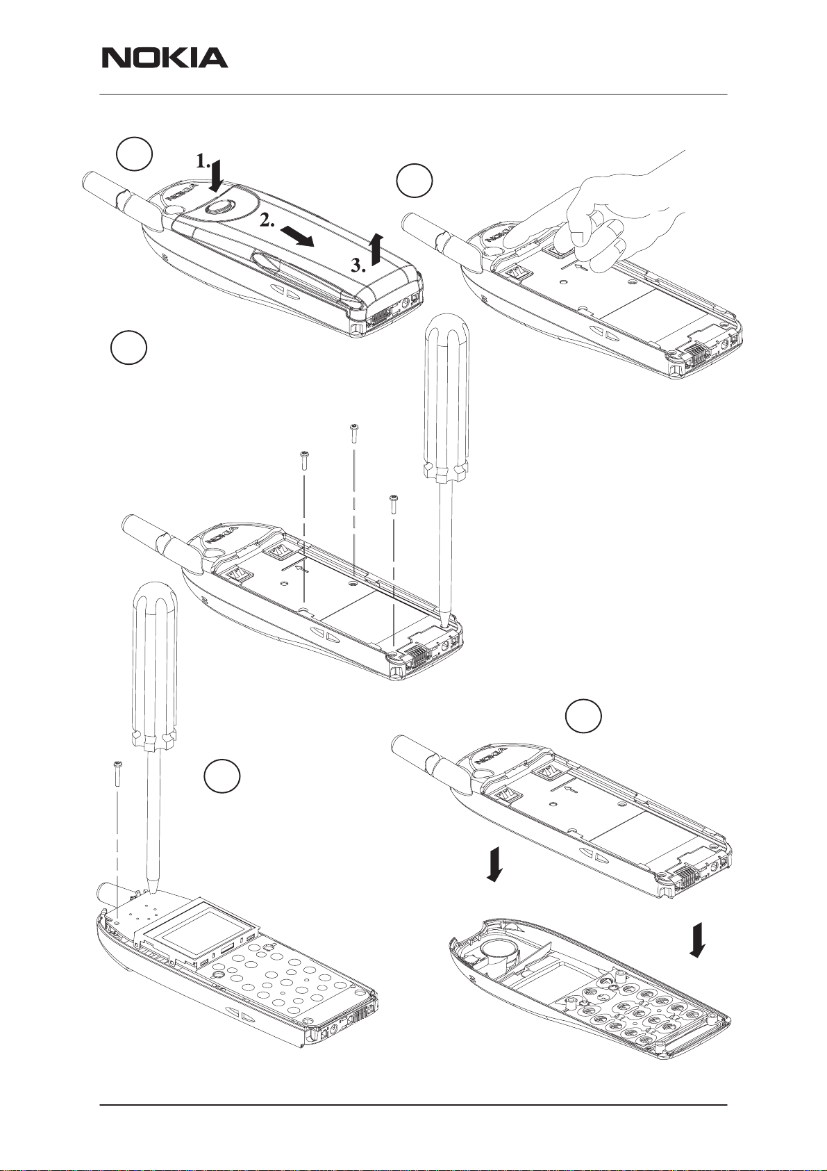
NOTE: Do not attempt to remove the antenna from the B–cover.
NSD–3
Disassembly / Troubleshooting Instructions
1.
Remove battery
3.
Remove back cover screws (4pcs).
NOTE! When assembling the B
cover screws, use 17 Ncm torque.
Remove dust cap
2.
by finger nail
Turn around and remove
UI module screws (2 pcs)
Issue 1 06/1999
5.
4.
Carefully remove A–cover, keymat, power keymat and speaker will follow. Note snap fixings !
Nokia Mobile Phones Ltd.
Page 3
Page 4
NSD–3
Disassembly / Troubleshooting Instructions
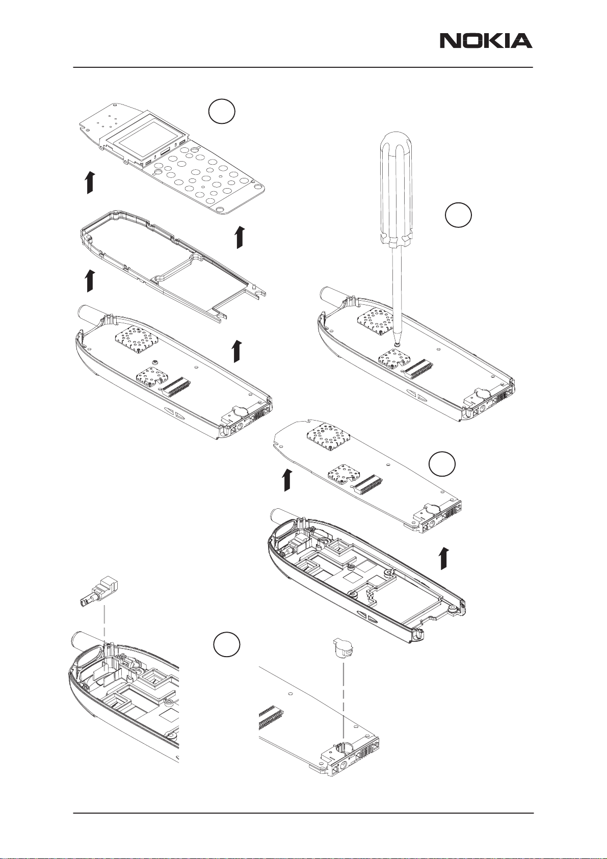
6.
Remove UI–module and frame.
PAMS Technical Documentation
7.
Remove engine module screw (1 pc).
NOTE! When assembling the screw use
17 Ncm torque.
Remove vibra motor.
9.
8.
Remove engine module
Remove microphone
Page 4
Nokia Mobile Phones Ltd.
Issue 1 06/1999
Page 5

PAMS Technical Documentation
Disassembly / Troubleshooting Instructions
Trouble Shooting
Baseband Troubleshooting
Each main portion of the circuit will be described in enough detail for the
troubleshooter to determine whether or not that part of the circuit being
evaluated is functional. It will be helpful to use the placement diagram,
which illustrates all of the necessary testpoints in the baseband circuit, to
troubleshoot the phone. The placement diagram is intended to be used
concurrently with this document.
Main Circuit Sections
Power Circuitry
NSD–3
There are two ASICs in the baseband section, which supply power to
most of the phone. CCONT is the main power management ASIC, and
PENTA is used to supply additional switchable regulators for use in RF.
Two discrete linear regulators are used as well.
CCONT
CCONT is the main power management ASIC. It’s features include eight
2.8V linear regulators, a linear regulator with adjustable output, a reference voltage output, a 5V switch mode regulator, an 8 channel A/D converter, and 32kHz clock circuitry. Each of the main functions and signals
are described below, including information on how to verify correct operation.
Vbat
CCONT is powered directly from the battery voltage, Vbat. Since CCONT
is a uBGA, the physical connection of CCONTs power pins can not be verified. Vbat must be checked instead at the closest external component,
which is shown as TP1. Valid voltages are 3.1–4.1V and should always be
powered; assuming voltage is applied to the battery terminals.
Vref
Vref is used as a reference voltage both internal and external to CCONT. It
is switchable between the nominal voltages of 1.500V and 1.251V, with
the default at power up being 1.500V. The phone uses the 1.251V reference, so once flash software is running Vref should switch to 1.251V.
Check Vref at TP2. Valid voltages are 1.478 – 1.523V and 1.244 – 1.258V,
respectively.
Linear Regulators
1. Vbb
Issue 1 06/1999
Nokia Mobile Phones Ltd.
Page 5
Page 6

NSD–3
Disassembly / Troubleshooting Instructions
Vbb supplies power to most of the baseband circuitry. This regulator
should be on at all times during CCONTs power on, reset, and sleep
modes. Nominal voltage is 2.8V, but anything in the range 2.7–2.87V is
valid. Vbb is found at TP3.
2. RF Regulators (VR1–VR7)
VR1 through VR7 are referred to as the RF regulators. Most are switch-
able, and all should be within 2.67 – 2.85V when they are on (2.8V nominal). VR1 and VR6 are always on during CCONTs power on mode. The
rest of the regulators are switchable and are normally on during one or
more of the various phone states, but may be turned on at any time with
the service software in order to verify their output. The RF regulators can
be checked at the following test points.
a) VR1 – TP10
b) VR1_SW – TP11
c) VR2 – TP32
d) VR3 – TP30
e) VR4 – TP4
f) VR5 – TP31
g) VR6 – TP9
h) VR7 – TP33
PAMS Technical Documentation
3. V2V (VMAD)
The V2V regulator is intended to power the MAD4 ASIC core. The output
is adjustable from 1.3V to 2.65V in 0.225V steps, and is used with MAD4
ver 3 (but not MAD4 ver 2). The output at V2V when MAD4 ver 3 is
stuffed should be 1.750V ±5% and can be checked on TP2.
Switch mode regulator
1. V5V (+5V_POWER)
V5V is a 5V switch mode regulator, which always remains on during
CCONT power on mode. Valid voltages are 4.8V to 5.2V, and it can be
checked at TP13.
2. VSIM (3V_5V)
VSIM is powered by the same switch mode regulator as V5V, however, it
is switchable between 3V and 5V. The phone uses VSIM as the 3V
FLASH programming voltage, so it should remain off unless the phone is
being flashed. Valid voltages are 2.8V to 3.2V, and it can be checked at
TP7.
A/D Conversion
CCONT contains a 10–bit A/D converter that is multiplexed between 8 different inputs. They are used mainly for battery and charger monitoring.
The 8 inputs are Vbat (battery voltage), ICHAR (charger current), VCHAR
(charger voltage), BSI (battery type), BTEMP (battery temperature),
VCXOTEMP (PA temperature), RSSI (AMPS receive signal strength), and
EAD (accessory detection). These readings can be accessed through the
service software. Check for shorts or opens on the resistor networks connected to these signals if the flash align test software reports that they are
out of range.
Page 6
Nokia Mobile Phones Ltd.
Issue 1 06/1999
Page 7

PAMS Technical Documentation
Watchdog
CCONTs watchdog circuitry consists of an eight bit down counter that
causes CCONT to power down when zero is reached. The counter may
be reset by loading a new, non–zero value into the watchdog register via
CCONTs serial bus. It is difficult to verify the watchdog function, but the
serial bus may be verified.
There is a watchdog disable pin which allows the watchdog timer to expire without shutting down the phone, but this pin is mainly used as one of
the methods to turn on CCONT from power off mode. While the phone
power key is pressed, this pin should be pulled low and can be checked
at TP29.
The watchdog can be disabled by pulling down the above mentioned
pin(WDDISX) by installing a 0 Ohm resistor at R307, and removing R325.
Serial bus
Since the serial bus is used to control almost all of CCONTs functions,
any shorts or open circuits on these three lines would cause CCONT to
be completely nonfunctional. The main symptoms are the following:
CCONT will turn on when the power key is pressed (verify this by checking Vbb), but will then power off after 32 seconds. All three serial bus signals (CCONTCSX, UIF_CCONT_SDIO, and UIF_CCONT_SCLK) should
toggle when attempting to write to a CCONT register.
NSD–3
Disassembly / Troubleshooting Instructions
Note: If the LCD does not come on during this time, however, it may indicate that the serial bus is functional, but phone does not have valid flash
code.
PENTA
PENTA supplies power to the RF section. It has 5 independently switchable regulators that are controlled via separate enable pins. There is also
a common enable pin that must be active in order to turn on any of the
regulators. Each of the regulators, P1–P5, should have output voltages
between 2.7V and 2.85V (2.8V nominal). These can be checked at the following test points.
a) P1 – TP16
b) P2 – TP15
c) P3 – TP17
d) P4 – TP18
e) P5 – TP19
External regulators
There are three regulators used in addition to CCONT and PENTA. One
is controlled by CCONTs VR7 regulator output and used as a low noise
power source for RF. This regulator is 2.8V nominal and can be checked
at TP8.
The second regulator is used to power the data cable accessory, so output is enabled only when a data cable accessory is detected. This regulator is also 2.8V nominal and can be checked at TP42 (shares SGND).
Issue 1 06/1999
Nokia Mobile Phones Ltd.
Page 7
Page 8

NSD–3
Disassembly / Troubleshooting Instructions
The third regulator is used to power the DSP portion of MAD4. It is enabled by Vbb, and difference between the rise times of the DSP regulator
and Vbb should be less than 200usec. This regulator is 2.8V nominal and
can be checked on pin 1, 30, or 115 of the MAD4 ASIC.
Clocks
Sleep Clock
The 32kHz sleep clock is generated by CCONT, and can be checked at
TP26. The 32kHz square wave will be present only after the phone is
turned on. If no signal is present on this line, check the output of the oscillator at R304. This signal should be a 2Vp–p clipped signal riding on 1.5V
DC.
System Clock
The 19.2MHz system clock is generated by the VCTXO in the RF section,
and then squared in CAFE. Check TP20, which should be approximately
a 0.5V sinewave riding on 1.8V DC. Check TP22, which should be a 2.8V
squarewave. This clock is not active during the phone’s sleep mode
(CLK_EN is low during sleep mode).
PAMS Technical Documentation
CDMA clock
The CDMA clock is 9.8MHz and is generated in CAFE with a PLL. This
should be a 2.8V square wave and can be verified at TP21.
Charging Circuit
The charging switch, CHAPS, is controlled by a PWM from CCCONT.
This PWM can be at 1Hz or at 32Hz, with varying duty cycles, and should
only be active when a charger is detected. The frequency should be 1Hz
when an ACP–7 is detected and 32Hz when an ACP–9 is detected. To
verify correct operation of CHAPS, monitor the charging current (ICHAR)
with the service software. When the PWM is off, current should be
approximately 200uA. When the PWM is on, it should be greater than
approximately 300mA.
CAFE
The CAFE ASIC performs various functions with respect to the RF circuitry and audio. It digitizes the analog voice signals from the microphone as
well as converts received digital data to voice signals to be sent to the earpiece. This also includes accessory microphones and speakers. It also
generates and decodes I and Q data for CDMA, and demodulates FM
(AMPS) signals. CAFE also acts as a clock squaring circuit and CDMA
clock generator.
Page 8
Microphones
The internal microphone is biased using transistor V201, which is powered by VR1_SW (TP11 2.75VDC). Check also the output of V201).
Nokia Mobile Phones Ltd.
Issue 1 06/1999
Page 9

PAMS Technical Documentation
V201, R220 and C212 should be installed, and R202 should not be
installed. MICP should be about 1.7VDC, and MICN should be about
0.4VDC. Internal microphone bias should only be active during a call.
The XMIC is biased by the AUXOUT signal (pin 75) through R209 and
R208. The output voltage at pin 75 is about 1.5V.
Earpiece and XEAR
The internal earpiece is driven differentially from pins 77 and 80 (EARP
and EARN). The DC voltage on these two pins is 1.35V. The difference
in the DC voltage between these two pins should not be more than 50mV.
The XEAR signal drives audio to the external accessories. The CAFE
signal name is HF (pin 81). The DC level on this pin should be 1.35V.
HFCM (pin 82) should also be at 1.35V. The difference in DC voltage between these two pins should not be more than 50mV.
Note that SGND is the return path for XMIC and XEAR.
Clock circuit
A 19.2MHz sinusoid should appear on pin 25 (Also TP20). This is from
the VCTCXO in the RF. The CAFE will then produce a 19.2MHz clock at
pin 18 (TP22), and a 9.83MHz clock on pin 19 (TP21). See also Clocks
section.
NSD–3
Disassembly / Troubleshooting Instructions
MAD4
AMPSMOD
AMPSMOD is the voice signal to modulate (FM) the RF carrier for transmission. It is the voice signal that has been processed by the DSP
(MAD4) for transmission in AMPS mode. It represents a modified version
of the signal produced by the microphone (CAFÉ pin 58).
Transmit and Receive RF Signals
In CDMA mode, receive I and Q channel RF signals [RXIQ(3:0)] come
into CAFÉ at pins 44, 45, 47, and 48. C207, C208, C209, and C210 can
also be checked for these signals since they are in series with the CAFÉ
pins. Transmit I and Q RF signals [TXIQ(3:0)] can be seen at pins 55, 56,
59, and 60 and C201, C204, C222, and C224.
In AMPS mode, the modulated receive RF signals (LIM_P and LIM_N)
can be seen coming into pins 23 and 24 and C216 and C217. For the
AMPS Transmit signal, see AMPSMOD above.
The MAD4 ASIC is the core of the baseband functionality and basically
contains the DSP, MCU, and CDMA logic. The DSP is used to perform
functions such as RF control, DTMF tone generation, and it implements
the vocoder. The MCU is used to perform functions that do not require as
much power. These are higher level functions such as UI software (key
presses, backlighting, LCD functions, etc.) and mode control.
DSP
The DSP sends control signals to the RF via PDMs. In order to control
RF parameters such as TX_VCO_CAL or TX_LIM_ADJUST, a continu-
Issue 1 06/1999
Nokia Mobile Phones Ltd.
Page 9
Page 10

NSD–3
Disassembly / Troubleshooting Instructions
ously variable analog signal must be used. Since the DSP outputs only
digital signals, a PDM RC circuit is used to convert the digital output signal to an average analog voltage. A PDM line will always have a series
resistor followed by a shunt capacitor. The output of the MAD4 PDM lines
will appear as squarewave signals. However, after the shunt capacitor the
signals will appear to be DC with perhaps a slight ripple. The RC circuit
acts as an integrator in order to yield the average value (DC) of the
squarewave signal.
The transmit data bus (TXD(7:0)) is 8 bits wide. In CDMA this bus is multiplexed between sending I and Q data. The signals required to transfer
TX data are TXGATE, CLK9M80, and IQSEL. TXGATE must be high to
transfer data, and the data is clocked by CLK9M80, which is running at
9.8MHz. In AMPS mode, CLK9M80 is running at 120kHz, therefore, data
is being transferred from MAD4 to CAFE at 120kHz.
The JTAG lines are intended to be used to operate the DSP (and/or
MCU) externally.
External Regulator
PAMS Technical Documentation
Failures
A separate 2.8V external regulator was added to power the Lead (DSP)
independently due to noise on VBB. Eventually, the next version of MAD4
will be used and the Lead may be powered by VMAD from CCONT. See
External Regulators section under CCONT/Linear Regulators. Note: This
regulator is also mentioned in section Power Circuitry.
MCU
The MCU is used to perform functions that require less processing power
than the DSP. It runs UI software, mode control, interfaces to MBUS,
downloads code to flash, reads and writes the EEPROM, controls charging, and interprets A/D data from CCONT.
Memories
MAD4 interfaces to three memories—Flash, SRAM, and EEPROM. All of
them are powered by 2.8V (Vbb). During Flash programming, Vpp (signal
name is Vff on schematic) is driven with 12V in the factory, and 3V at the
PC flash stations.
Most of the failures will be due to SMD errors. Either solder got where it
wasn’t supposed to be, parts slid off their pads, or possibly the parts were
placed incorrectly. A good visual inspection will uncover a large percentage of failing phones.
Won’t power up
Do a visual inspection. Verify that all parts are on the board correctly, and
that none are missing.
Check that the 32kHz clock turns on when attempting to power up.
Check the power circuitry. This includes VBAT, Vref, and all of the linear
regulators, as well as the Penta regulators. Verify also that the external
regulator that powers MAD4 (LEADVCC) is functional.
Page 10
Nokia Mobile Phones Ltd.
Issue 1 06/1999
Page 11

PAMS Technical Documentation
Flash Align
Test 9
High current: This indicates that the problem is likely caused by a shorted
component. Check orientation of major components (including RF), and
check for shorts. Likely components are those which are powered directly
from Vbat such as CCONT, the PAs, and various capacitors.
Low current: This indicates that CCONT is not powering on. Verify
CCONT circuitry.
Test 10
Flash: Failure to flash is the main baseband failure. Check all the CCONT
regulators, especially Vbb, VR1, and VR6 for shorts. Check clocks and
reset circuitry. Check for shorts on the address, data, and chip enable
lines on the memories and MAD4. If a short is detected, it may be that it is
beneath the BGA flash and may have to be replaced.
NOTE: Unfortunately, there is no ROM software that can be run when the
phone does not flash. Typically, this software would be used to test all of
the interfaces between MAD4 and its peripherals. Therefore, it must be
visually (or by Ohmmeter) determined whether there is a possible short
between two or more of the address or data lines.
NSD–3
Disassembly / Troubleshooting Instructions
In the field
Solder joints may be adequate for passing manufacturing requirements,
however, they may not hold up to mechanical stress or heat cycling.
Cracked or broken solder may cause failures to occur from simple use.
Reflowing some of the major components may fix problems where the
phone exhibits strange behavior (some buttons may not work, the phone
may not ring, etc.) or may not power on anymore.
Battery will not charge
If the battery won’t charge (phone won’t allow the battery to charge),
check CHAPS and the charging circuit. It may also be necessary to verify
the A/D functionality of CCONT since this is the method of detecting battery type, charger type, etc
Audio failures
If audio fails to be heard from the earpiece (or XEAR), it could be a number of possible problems. Check the following:
Check earpiece contacts.
Verify that the CAFÉ EARP and EARN bias is on. If necessary, check the
entire receive path—Rx voice data comes from the RF through the RXIQ
bus (CDMA) or LIM_P and LIM_N (AMPS), then to MAD4 through RXD
(11:0) (Refer to schematic). See the Baseband section of the Service
Manual for more detail on RXD bus usage.
The Rx voice data then goes back to CAFE on CAFESIO (0), and then to
the earpiece or XEAR. CAFESIO (2) must also be active.
Issue 1 06/1999
Nokia Mobile Phones Ltd.
Page 11
Page 12
NSD–3
Disassembly / Troubleshooting Instructions
Conversely, if the transmit audio is not working, the fault could be anywhere in the transmit path. Check the following:
Check microphone contacts.
Microphone bias.
Tx voice data is transferred from CAFÉ to MAD4 on CAFESIO (1). CAFE-
SIO (2) must also be active. Tx voice data is then sent back to CAFÉ on
the TXD bus (See schematic). See the Baseband section of the Service
Manual for more detail on RXD bus usage.
Tx voice data is then sent to RF on the TXIQ bus (CDMA) or AMPSMOD
(AMPS).
PAMS Technical Documentation
Test Point Desig-
nator
31 SleepClock 32.768 KHz typical Square waveform From CCONT to MAD4
25 Clk19m20 19.2 MHz Square waveform From CAFÉ to MAD4
23 Clk19M2rf (D201–25) 19.2 MHz Sinusoidal waveform From RF Synthesizer to CAFÉ and other RF Synthesiz-
24 Clk9m8 9.8 MHz Square waveform From CAFÉ to MAD4
36 CRB 32Khz – 2.8V From 32K crystal to CCONT
14 MemRdX 0 / 2.8 V (active low) From MAD4 to Flash and RAM output enables
15 MemWrx 0 / 2.8 V (active low) From MAD4 to Flash and RAM write enables
13 ROM1SelX 0 / 2.8 V (active low) From MAD4 to Flash chip enable
5 Clk_En 0 / 2.8 From MAD4 to FLASH, CCONT and CAFE
1 PurX ( D101–116 ) 0 / 2.8 V (active low) From CCONT to MAD4
35 WdDisX 2.8 V (active low) CCONT test point for phone diagnosis mode
34 PwrOnX 0 / 2.8 V (active low) From UI Power Key to MAD4 and CCONT
33 ResetX 0 / 2.8 V (active low) From MAD4 to CAFE
30 Vbat 3.1 – 4.1 V valid battery range
3 Vbb 2.8 V typical (2.7 – 2.87 V) From CCONT to MAD4 and Memories
2 Vmad N / A From CCONT to MAD4
11 Vr1 2.8 V typical (2.67 –2.85 V) From CCONT to 19.2MHz VCTCXO
12 Vr1_Sw (MIC bias) 0 / 2.75V From CCONT to V201 to CAFE
40 Vr2 0 / 2.8 V typical (2.67 –2.85 V) From CCONT to CELL Receiver
38 Vr3 0 / 2.8 V typical (2.67 –2.85 V) From CCONT to RF Receiver
4 Vr4 2.8 V typical (2.67 –2.85 V) From CCONT to PCS Transmitter
39 Vr5 0 / 2.8 V typical (2.67 –2.85 V) From CCONT to CELL Transmitter
10 Vr6 2.8 V typical (2.67 –2.85 V) From CCONT to CAFE
41 Vr7 0 / 2.8 V typical (2.67 –2.85 V) From CCONT to RF Synthesizer
9 Vr7a 0 / 2.8 V
6 Vref 1.251 typical (1.244 – 1.258) From CCONT to CAFE
16 +5_Power (V5V) 5 V typical (4.8 – 5.2 V) From CCONT to CELL and PCS Transmitters
7 3V_5V (VSIM) 0 / 2.8 – 3.2 V From CCONT to Flash
18 P1 0 / 2.8 V typical (2.7 – 2.85) From PENTA to CELL Synthesizer
17 P2 0 / 2.8 V typical (2.7 – 2.85) From PENTA to AMPS Receiver
19 P3 0 / 2.8 V typical (2.7 – 2.85) From PENTA to PCS Synthesizer
21 P4 0 / 2.8 V typical (2.7 – 2.85) From PENTA to CELL Receiver
22 P5 0 / 2.8 V typical (2.7 – 2.85) From PENTA to PCS Receiver
43 V_in ACP–7: 3.5VAC(rms) to 8.5VAC(rms)
44 L_Gnd 0V From Bottom Connector, through an inductor to Phone
45 V_in ACP–7: 3.5VAC(rms) to 8.5VAC(rms)
46 Chrg_Ctrl 0 / 2.8 V From MAD4 to CHAPS
47 Chrg_Ctrl 0 / 2.8 V From MAD4 to CHAPS
Signal Name General
Characteristics
(3.1 – 5.2 with charger connected)
ACP–9 : 4.3VDC to 8VDC
ACP–9 : 4.3VDC to 8VDC
General Signal Destination
ers
From Battery connector to CCONT and other various
parts of phone
From Bottom Connector to CHAPS
Note: Lower VBA T = lower Vin levels
Ground
From Bottom Connector to CHAPS
Note: Lower VBA T = lower Vin levels
Page 12
Nokia Mobile Phones Ltd.
Issue 1 06/1999
Page 13

PAMS Technical Documentation
NSD–3
Disassembly / Troubleshooting Instructions
48 MicP
49 MicN
50 Xmic
51 Sgnd
52 Xear
53 Mbus 0 / 2.8 V Bi–directional Serial bus to MAD4 and the Bottom Con-
54 Fbus_Rx 0 / 2.8 V Serial bus from Bottom Connector to MAD4
55 Fbus_Tx 0 / 2.8 V Serial bus from MAD4 to the Bottom Connector
56 L_Gnd 0V From Bottom Connector, through an inductor to Phone
37 BTEMP Variable DC From Battery terminal to CCONT
42 VCHAR Vin divided by 10 From System connector to CHAPS and CCONT
8 PA_Temp Variable DC From Shark thermister to CCONT A/D
20 Vibra 0 / 2.8 (11Khz when Vibra active) From MAD4 to V ibra Motor
29 EEPROMsclk 0 / 2.8 From MAD4 to EEPROM
28 EEPROMsda 0 / 2.8 From MAD4 to EEPROM
32 Amps_Mod Analog data (voice) From CAFÉ to RF section
26 Address (23:0) 0 / 2.8 V From MAD4 to Flash and RAM
27 Data (15:0) 0 / 2.8 V From MAD4 to Flash and RAM
1.7VDC (no voice activity)
0.4VDC (no voice activity)
0.9VDC (no voice activity)
Approximately 0.0V
2.8VDC (no voice activity)
From Bottom Connector to CAFÉ internal microphone
input
From Bottom Connector to CAFÉ internal microphone
input
From Bottom connector to CAFÉ external microphone
input
From CAFÉ to Bottom Connector
From CAFE to Bottom Connector
nector
Ground
Issue 1 06/1999
Nokia Mobile Phones Ltd.
Page 13
Page 14

NSD–3
Disassembly / Troubleshooting Instructions
PAMS Technical Documentation
Page 14
Nokia Mobile Phones Ltd.
Issue 1 06/1999
Page 15

PAMS Technical Documentation
RF Troubleshooting
This document is written for use in conjunction with the WinTesla Tuning
and Testing software. Pictures of the menu structures are shown through
out the document. This document should be used in conjunction with the
phone’s schematics which are referred to in detail throughout.
WinTesla has 3 key menus:
onfigure Basic set up covered in WinTesla General Set Up
C
sting This menu allows switching on the phone in different modes
Te
T
uning This menu allows tuning and storing of data to eeprom
Tuning is described in four parts:
A description of the tuning: Describes the tuning process
Definition of result: What tuning is storing to eeprom
Manual Verification: How to use WinTesla to tune the phone
NSD–3
Disassembly / Troubleshooting Instructions
Trouble Shooting: Outlines key components to be checked
WinTesla General Set Up
Connect the phone to the PC COM port and start WinTesla. Select “Product” and “New” and the phone configuration will be selected automatically.
Select “Configure” and “Frequency Plan”. You will then be able to see and
also change the default AMPS and CDMA Channels. The cable loss
should also be entered here.
Note: It is possible to enter a Tx and Rx cable loss separately, however if
a single cable is being used then both losses should be the same. Also
the loss will be different for the 1900MHz band and the 800MHz band
hence sections for both.
Issue 1 06/1999
Nokia Mobile Phones Ltd.
Page 15
Page 16

NSD–3
Disassembly / Troubleshooting Instructions
PAMS Technical Documentation
Page 16
Nokia Mobile Phones Ltd.
Issue 1 06/1999
Page 17

PAMS Technical Documentation
Testing Menu
AMPS Fault Finding Setup
For all AMPS transmitter and receiver testing and trouble shooting select
“Testing” and then “AMPS/Baseband Tuning”. This automatically sets the
receiver on and the transmitter on Channel 380 Power level 3.
NSD–3
Disassembly / Troubleshooting Instructions
The transmitter power level can be set by selecting the “Power Level”.
The TX_LIM_ADJ and other PDMs can be adjusted by selecting “PDM
Ctrl”.
Issue 1 06/1999
Nokia Mobile Phones Ltd.
Page 17
Page 18

NSD–3
Disassembly / Troubleshooting Instructions
Cell Band CDMA Fault Finding Setup
Both 1900MHz and 800MHz CDMA is started from the same selection of
“Testing” and “CDMA”. Entering this screen switches on both the transmitter and receiver on Channel 364. For PCS simply click the PCS box. The
PDMs can be adjusted with the slider or by entering a value. The transmitter is switched off by clicking the “Tx Off” Box. The RX_IF_AGC is read
by clicking the “Read” button. The LNA defaults to ON and OFF can be
switch by ticking the “LNA” box.
PAMS Technical Documentation
Page 18
Nokia Mobile Phones Ltd.
Issue 1 06/1999
Page 19

PAMS Technical Documentation
Disassembly / Troubleshooting Instructions
PCS Band CDMA Fault Finding Setup
Use the same Testing menu as Cell CDMA, once in the CDMA Testing
Window click PCS in the top left hand corner. See previous section.
Tuning Menu
The tuning menu is divided into the following sections:
Battery
AMPS
800 CDMA
1900 PCS
In all the tunings WinTesla will prompt you with the equipment settings. At
the end of the tuning WinTesla will give you the option to save the new
tuning values to EEPROM or to exit without saving new values to EEPROM.
NSD–3
AMPS Tuning AFC
Description of Test
This test tunes the VCTCXO to exactly 19.2 MHz using a DC voltage
(TP100) controlled by the AFC PDM. The resulting PDM is stored to eeprom. The unmodulated AMPS transmitter is set on Channel. The output
carrier is monitored with a spectrum analyzer. Click on WinTesla H
equipment set up. The AFC PDM is tuned until the RF carrier frequency is
within ±250Hz of 841.5MHz (i.e. Channel 550). The AFC must be tuned if
the VCTCXO is replaced.
On SSP Phones where there is no AMPS the PCS Transmitter is used
however the CDMA IQ modulation is switched off and the AFC is tuned
on the CW carrier.
NOTE: The Spectrum Analyzer must be connected to a high stability
10MHz reference at the rear of the instrument, if this is not done then the
tuning will not be accurate.
Definition of Result
The result of this tuning is the AFC PDM stored to eeprom which puts the
VCTCXO at the correct frequency.
elp for
Manual Verification
Use WinTesla as follows:
Issue 1 06/1999
Nokia Mobile Phones Ltd.
Page 19
Page 20

NSD–3
Disassembly / Troubleshooting Instructions
PAMS Technical Documentation
Trouble Shooting
The VCTCXO reference designator is G501. VR1 is supplies 2.7v to the
VCTCXO (TP101) through R501 and decoupled with C561. The VCTCXO
is controlled by a DC level from the AFC PDM in MAD connected to Pin
132. The PDM is filtered by R114 and C130 in the base band section and
by R504 and C507 in the RF section. Resistors R503 and R538 center
the PDM voltage. Typically a correctly tuned VCTCXO should have
approximately 2 volts on pin 1 (TP100).
Adjustment of the AFC PDM from 0 to 511 should result in a voltage
change on G501 Pin 1 (TP100) between 1.9 and 2.2 volts with a 10KHz
change in the transmitter output frequency in Cel or a 22KHz change in
PCS.
On SSP phones which do not have AMPS, clicking the “PCS AFC Tuning
On” box will disable the CDMA modulation allowing AFC tuning to be performed on the RF carrier feed through.
Page 20
Nokia Mobile Phones Ltd.
Issue 1 06/1999
Page 21

PAMS Technical Documentation
19.2MHz measured at the output of the VCTCXO Buffer (TP102) with a
10 Mohm probe.
NSD–3
Disassembly / Troubleshooting Instructions
AMPS Tuning Tx Power Levels
Description of Test
These tests tune all the AMPS power levels 2 to 7 to the required output
power level by changing the TX_LIM_ADJ PDM (TP103). This is done
with the phone in AMPS mode with transmitter on and the TX_RF_AGC
PDM set to FF and TX_IF_AGC set to 1FF.
NOTE: The AMPS Transmitter band is frequency compensated with fixed
values, these are referenced to the channel with the lowest loss which is
Channel 550. It is very important to tune the transmitter using Channel
550 otherwise the maximum allowable power may be exceeded.
Definition of Result
When all the power levels have been correctly tuned the values of
TX_LIM_ADJ PDM are stored in eeprom
RF_TUNE_AMPS_TX_LIM_ADJ_HANDLE.
Manual Verification
Use WinTesla as follows:
Issue 1 06/1999
Nokia Mobile Phones Ltd.
Page 21
Page 22

NSD–3
Disassembly / Troubleshooting Instructions
PAMS Technical Documentation
NOTE: This window was taken from WinTesla with the cable loss set at
0.7dB. The power levels tuned at the phones RF connector are:
Power Level Nominal Power Range
0–2 25.05 dBm +/– 0.15 dB
3 24 dBm +/– 0.5 dB
4 20 dBm +/– 0.5 dB
5 16 dBm +/– 0.5 dB
6 12 dBm +/– 0.5 dB
7 8 dBm +/– 1 dB
Trouble Shooting
If only the top PL2 or PL3 power levels fail then the transmitter is slightly
short of gain. This could be caused by many transmitter faults. Check the
PA N605 output Pins 11,12,13,14 (TP104) are not shorted to ground.
Note: This should be done with the phone switched off. If these pins
(TP104) are shorted the PA must be replaced, and it is likely that inductor
L618 will have burnt out and become open circuit. Also check that the Tx
VHF LO (TP105) and UHF LO (TP106) are present at the correct frequency and level (see below).
Page 22
Nokia Mobile Phones Ltd.
Issue 1 06/1999
Page 23

PAMS Technical Documentation
Tx VHF LO Measured at TIF N604 Pin 3 (TP105) with a Hi Z Probe:
NSD–3
Disassembly / Troubleshooting Instructions
UHF Cel LO measured at Odyssey N703 Pin 2 (TP106) with Hi Z probe
when set to Channel 384:
Issue 1 06/1999
Nokia Mobile Phones Ltd.
Page 23
Page 24

NSD–3
Disassembly / Troubleshooting Instructions
AMPS Tuning Tx Modulation Index
Description of Test
This test tunes the Gain in the DSP so that the amplitude of TX_MOD going into the Tx VHF VCO produces the correct peak deviation of the RF.
Click the WinTesla H
elp button for equipment set up.
Definition of Result
The result is the DSP Gain, which gives 2KHz +/–0.05KHz peak deviation
at the RF output. This DSP Gain is stored to eeprom.
Manual Verification
Use WinTesla as follows:
PAMS Technical Documentation
Page 24
Trouble Shooting
Check the following components in the Tx VHF VCO to see if they are
damaged V501, V504, V508, V511 and L504.
NOTE: If any of these components are replaced then the Tx Modulation
Index must be re–tuned.
Nokia Mobile Phones Ltd.
Issue 1 06/1999
Page 25

PAMS Technical Documentation
AMPS Tuning RSSI
Description of Test
Changing the AMPS receiver input level results in different Gains in the
Limiting amplifier in RIF to produce a limited output. This test measures
AMPS RSSI with high receiver input signal and low receiver input signal,
and then stores these values to eeprom. WinTesla will prompt with what
level to set going into the receiver.
Definition of Result
The reported result is the ADC value from CCONT. For RSSI Lo the result
should be between 570 and 970 and is stored to eeprom under the handle RF_TUNE_AMPS_RSSI_LO_HANDLE. For RSSI Hi result should be
between 750 and 1050 and is stored to eeprom under the handle
RF_TUNE_AMPS_RSSI_HI_HANDLE.
Manual Verification
Use WinTesla as follows:
NSD–3
Disassembly / Troubleshooting Instructions
Trouble Shooting
Check components in the AMPS receiver chain starting with the Duplexer
Z701, Down Converter IC N703, 128.55MHz IF SAW filter Z702, 450KHz
Ceramic filters Z706 and Z708 and RIF N702. Check the Rx VHF LO RIF
N702 Pin 20 (TP107) see below. Also check RIF 450KHz output LIM_P
Measured at RIF Pin 17 (TP108) and the RSSI voltage at RIF N702 Pin
16 (TP109) which indicates the signal level into the receiver.
Rx VHF LO Measured at RIF N702 Pin 20 (TP107) with a Hi Z Probe:
Issue 1 06/1999
Nokia Mobile Phones Ltd.
Page 25
Page 26

NSD–3
Disassembly / Troubleshooting Instructions
PAMS Technical Documentation
LIM_P Measured at RIF Pin 17 (TP108) with a 10 Mohm probe:
Page 26
Nokia Mobile Phones Ltd.
Issue 1 06/1999
Page 27

PAMS Technical Documentation
RSSI Voltage at RIF N702 Pin 16 (TP109) versus Rx Power at RF connector:
NSD–3
Disassembly / Troubleshooting Instructions
AMPS Tuning Rx Audio Gain
Description of Test
This test tunes the DSP Gain so that an RF input signal with 2.9KHz deviation and 1KHz modulation results in a voltage at the receiver output of
57.4 +/–3 mV RMS. The DSP Gain is then stored to eeprom.
Definition of Result
The stored eeprom value will result in 57.4mV RMS at XEAR when using
JBA4 and receiving an RF signal with 1KHz tone and 2.9KHz deviation.
Manual Verification
Use WinTesla as follows:
Issue 1 06/1999
Nokia Mobile Phones Ltd.
Page 27
Page 28

NSD–3
Disassembly / Troubleshooting Instructions
Trouble Shooting
Verify that the signal on RIF N702 Pin 17 (TP108) shown in the plot
above is present on CAFÉ Pin 24 (TP110). If this is the case then check
the test set up.
PAMS Technical Documentation
800 CDMA Tuning Tx IF AGC
Description of Test
The RIF and TIF AGC is approximately a second order curve, this curve
is split into 16 segments for both Transmitter and Receiver. Offset and
slope values are stored in eeprom for each of these 16 segments. The
offset for the segments is computed from the 3–point calibration performed in this test. After test a 2
Offset and Slope computed.
TX_IF_AGC must be adjusted to achieve the correct power level for Point
1, when this is done the process must be repeated for Points 2 and 3.
Definition of Result
The results of the 3 point tuning are the 16 slope and offset values, which
are stored to eeprom RF_TUNE_CELL_TX_AGC_OFFSET_SLOPE_HANDLE.
Manual Verification
Use WinTesla as follows:
nd
order approximation is made and the
Page 28
Nokia Mobile Phones Ltd.
Issue 1 06/1999
Page 29

PAMS Technical Documentation
Trouble Shooting
If this tuning fails it is probably the highest power level indicating that
there is a gain loss in the transmitter path. This could be caused by many
transmitter faults. Check the PA N605 output Pins 11,12,13,14 (TP104)
are not shorted to ground. Note this should be done with the phone
switched off. If these pins are shorted the PA must be replaced, and it is
likely that inductor L618 will have burnt out. Also check that the Tx VHF
LO (TP105) and UHF LO (TP106) are present at the correct frequency
and level (see the A
NSD–3
Disassembly / Troubleshooting Instructions
MPS Tuning Tx Power Levels section).
NOTE: If any of these components are damaged and are replaced then
the T
x IF AGC must be retuned.
Tx Output spectrum at RF Connector with 30dB attenuator on Spectrum
Analyzer:
Issue 1 06/1999
Nokia Mobile Phones Ltd.
Page 29
Page 30

NSD–3
Disassembly / Troubleshooting Instructions
Tx Output spectrum at RF Connector with 30dB attenuator on Spectrum
Analyzer:
PAMS Technical Documentation
800 CDMA Tuning LNA Switch
Description of Test
In this test the phone is set to continuous receive mode, a CW signal is
put into the receiver via the RF connector. WinTesla with indicated the
amplitude. There is a frequency offset of 300KHz from the center of the
receiver. The RX_IF_AGC is adjusted by the phones software to make
the best use of the CAFÉ ADC. The setting of RX_IF_AGC is then read
from the phone. The LNA is switched from High Gain mode to Low Gain
Mode. The RX_IF_AGC is allowed to readjust itself to again make the
best use of the CAFÉ ADC and the RX_IF_AGC is read a second time.
The result is the Gain delta between High Gain and Low Gain modes.
Definition of Result
The displayed result is the High Gain – Low Gain delta in dB after applying the PDM difference to the previously computed 3–point curve fit. This
delta should be between 21 and 24dB. This is stored to eeprom handle
RF_TUNE_RX_GS_HANDLE.
Manual Verification
Page 30
Use WinTesla as follows:
Nokia Mobile Phones Ltd.
Issue 1 06/1999
Page 31

PAMS Technical Documentation
NSD–3
Disassembly / Troubleshooting Instructions
Trouble Shooting
Check that the RX_GS line on the up–converter N703 Pin 15 (TP111) is
changing from high to low. If this is and the Gain does not change significantly then the Up–converter IC N703 is probably faulty and should be
replaced.
800 CDMA Tuning Rx IF AGC
Description of Test
The RIF and TIF AGC is approximately a second order curve, this curve
is split into 16 segments for both Transmitter and Receiver. Offset and
slope values are stored in eeprom for each of these 16 segments. The
offset for the segments are computed from the 3–point calibration performed in this test. After test a 2
Offset and Slope are computed.
This tuning is done by putting signal level 1 into the receiver, the
RX_IF_AGC will then automatically adjust for max CAFÉ input and the
RX_IF_AGC is noted. This process is then repeated for signal levels 2
and 3.
nd
order approximation is made and the
Definition of Result
The results of the 3 point tuning are the 16 slope and offset values, which
are stored to eeprom RF_TUNE_CELL_RX_AGC_OFFSET_SLOPE_HANDLE.
Issue 1 06/1999
Nokia Mobile Phones Ltd.
Page 31
Page 32

NSD–3
Disassembly / Troubleshooting Instructions
Manual Verification
Use WinTesla as follows:
PAMS Technical Documentation
Trouble Shooting
Check components in the 800 MHz receiver chain, from the Duplexer
N701, Down converter N703, the 128.1MHz CDMA IF SAW filter Z704
and RFI N702. Check that the RX_IF_AGC RIF Pin 7 (TP112) changes as
the receiver input signal level is adjusted.
NOTE: If any of these components are damaged and are replaced then
x IF AGC second order curve must be retuned.
the R
800 CDMA Tuning Rx IF Compensation
Description of Test
In this tuning the receiver is calibrated at five different frequencies across
the band. WinTesla instructs the Signal Generator to be set at five specific
frequencies and a fixed amplitude. The RX_IF_AGC is adjusted by the
phones software to make the best use of the CAFÉ ADC. The setting of
RX_IF_AGC is then read from the phone at each of the five frequencies.
Definition of Result
The five different values of RX_IF_AGC are stored to EEPROM.
Page 32
Nokia Mobile Phones Ltd.
Issue 1 06/1999
Page 33

PAMS Technical Documentation
Manual Verification
Use WinTesla as follows:
NSD–3
Disassembly / Troubleshooting Instructions
Trouble Shooting
See section 800 CDMA Tuning Rx IF AGC
1900 CDMA Tuning Tx IF AGC
Description of Test
The RIF and TIF AGC is approximately a second order curve, this curve
is split into 16 segments for both Transmitter and Receiver, Offset and
slope values are stored in eeprom for each of these 16 segments. The
offset for the segments are computed from the 3–point calibration performed in this test, then a 2
and Slope computed.
TX_IF_AGC must be adjusted to achieve the correct power level for Point
1, when this is done the process must be repeated for Points 2 and 3.
Definition of Result
The results of the 3 point tuning are the 16 slope and offset values, which
are stored to eeprom RF_TUNE_PCS_TX_AGC_OFFSET_SLOPE_HANDLE.
nd
order approximation is made and the Offset
Issue 1 06/1999
Nokia Mobile Phones Ltd.
Page 33
Page 34

NSD–3
Disassembly / Troubleshooting Instructions
Manual Verification
Use WinTesla as follows:
PAMS Technical Documentation
Trouble Shooting
If this tuning fails it is probably the highest power level indicating that
there is a gain loss in the transmitter path. This could be caused by many
transmitter faults. Check the PA N606 output Pins 11,12,13 and 14
(TP113) are not shorted to ground. If this is the case PA must be replaced. Also it is likely that inductor L611 has burnt out and has open circuit. Check the switch to the split band filter N609 and it’s control transistor V614 and control line FILT_SEL (TP114). Check also the Up Converter, N601 and also TIF, N604. Also check that the Tx VHF LO (TP105) and
UHF LO (TP115) are present at the correct frequency and level.
NOTE: If any of these components are damaged and are replaced then
x IF AGC must be retuned.
the T
1900 CDMA Tuning LNA Switch
Description of Test
In this test the phone is set to continuous receive mode, a CW signal is
put into the receiver via the RF connector with amplitude of dBm and offset 300KHz from the center of the receiver. The RX_IF_AGC adjusts to
make the best use of the CAFÉ ADC. The setting of RX_IF_AGC is then
Page 34
Nokia Mobile Phones Ltd.
Issue 1 06/1999
Page 35

PAMS Technical Documentation
read from the phone. The LNA is switched from High Gain mode to Low
Gain Mode. The RX_IF_AGC is allowed to readjust itself to again make
the best use of the CAFÉ ADC and the RX_IF_AGC is read a second
time. The result is the Gain delta between High Gain and Low Gain
modes.
Definition of Result
The displayed result is the High Gain – Low Gain delta in dB after applying the PDM difference to the previously computed 3–point curve fit. This
delta should be between 21 and 30dB. It is stored to eeprom handle
RF_TUNE_RX_GS_HANDLE.
Manual Verification
Use WinTesla as follows:
NSD–3
Disassembly / Troubleshooting Instructions
Trouble Shooting
In the PCS band the RX_GS input to the up–converter N01 is NOT used.
Instead the external LNA is switched on and off with Penta N303 Pin 9
(output P5) (TP116). Check that the external LNA is being switched on
and off by probing. If this is the case then there is probably a fault with the
external LNA. Check the transistor V705 and it’s collector components
L710. Also check the bias circuitry V704 and L708.
NOTE: If any of these components are damaged and are replaced then
the R
Issue 1 06/1999
x IF AGC must be retuned.
Nokia Mobile Phones Ltd.
Page 35
Page 36

NSD–3
Disassembly / Troubleshooting Instructions
1900 CDMA Tuning Rx IF AGC
Description of Test
The RIF and TIF AGC is approximately a second order curve, this curve
is split into 16 segments for both Transmitter and Receiver. Offset and
slope values are stored in eeprom for each of these 16 segments. The
offset for the segments are computed from the 3–point calibration per-
nd
formed in this test, then a 2
and Slope computed.
This tuning is done by putting signal level 1 into the receiver, the
RX_IF_AGC will then automatically adjust for max CAFÉ input and the
RX_IF_AGC is noted. This process is then repeated for signal levels 2
and 3.
order approximation is made and the Offset
Definition of Result
The results of the 3 point tuning are the 16 slope and offset values which
are stored to eeprom RF_TUNE_PCS_RX_AGC_OFFSET_SLOPE_HANDLE.
PAMS Technical Documentation
Manual Verification
Use WinTesla as follows:
Page 36
Nokia Mobile Phones Ltd.
Issue 1 06/1999
Page 37

PAMS Technical Documentation
Disassembly / Troubleshooting Instructions
Trouble Shooting
Check components in the 1900 MHz receiver chain, from the Duplexer
N711, External LNA V705, Down converter N701, the 128.1MHz CDMA
IF SAW filter Z704 and RFI N702. Check that the RX_IF_AGC RIF Pin 7
(TP112) changes as the receiver input signal level is adjusted.
NOTE: If any of these components are damaged and are replaced then
x IF AGC must be retuned.
the R
1900 CDMA Tuning Rx IF Compensation
Description of Test
In this tuning the receiver is calibrated at six different frequencies across
the band. WinTesla instructs the Signal Generator to be set at six specific
frequencies and a fixed amplitude. The RX_IF_AGC is adjusted by the
phones software to make the best use of the CAFÉ ADC. The setting of
RX_IF_AGC is then read from the phone at each of the six frequencies.
Definition of Result
NSD–3
The five different values of RX_IF_AGC are stored to EEPROM.
Manual Verification
Use WinTesla as follows:
Trouble Shooting
See section 1900 CDMA Tuning Rx IF AGC.
Issue 1 06/1999
Nokia Mobile Phones Ltd.
Page 37
Page 38

NSD–3
Disassembly / Troubleshooting Instructions
Test Point values
NOTE: Test Point layout pictures are at the back of the binder.
PAMS Technical Documentation
Test Point
Designator
100 AFC VCTCXO Control voltage PDM from MAD4
101 VR1 2.7v supply to VCTCXO CCONT to VCTCXO
102 19.2 MHz 19.2 MHz from VCTCXO buff-erVCTCXO Buffer to CAFÉ and
103 TX_LIM_ADJ Detector demand voltage PDM from MAD4 Pin 128 de-
104 800 MHz PA
105 Tx VHF LO VHF LO to TIF
106 Tx UHF LO
107 Rx VHF LO 256.2 MHz VHF LO to RIF LO from PLL to RIF
108 LIM_P 450 KHz signal from RIF RIF 450 KHz output to CAFÉ
Signal Name General Characteristics General Signal Destination
PLL IC’s
tector circuit at RF output
Output
1 GHz
RF output from PA check for
short with phone switched
OFF
(PCS 416.2 MHz / CELL
CDMA 346.2 MHz / AMPS
347.1 MHz)
UHF LO to Odyssey up con-
verter IC
RF output from PA to Isolator
LO from PLL to TIF IC
LO from 1 GHz VCO to Odyssey up converter IC
109 RSSI dc voltage indicating signal
level into receiver
110 LIM_P 450 KHz signal into CAFÉ RIF 450 KHz output to CAFÉ
111 RX_GS 0v or 2.7v for LNA OFF or ON Voyager down converter LNA
112 RX_IF_AGC Dc voltage proportional to sig-
nal level into receiver in
CDMA mode
113 1900 MHz PA
Output
114 FILT_SEL 0v or 2.7v for PCS High band
115 Tx UHF LO
2GHz
116 Penta P5 0v or 2.7 from Penta P5 to
RF output from PA
Check for short with phone
switched OFF
or Low band
UHF LO to Apache
Up converter IC
PCS LNA for LNA OFF or ON
RIF output to CCONT Pin A1
A to D converter
control from MAD4 Pin 2
AGC control voltage from
MAD4 Pin 133 to RIF Pin 7
RF Output from PA to Isolator
Filter control line from MAD4
Pin 129
UHF LO from VCO to Apache
up converter N601 Pin 6
Control for PCS LNA from
Penta N303 Pin 9
Page 38
Nokia Mobile Phones Ltd.
Issue 1 06/1999
 Loading...