

Page 1
NPE-4 6310/NPL-1 6310i Repairhints
Customer Care Europe & Africa Version 1.0 Approved
SCCE Training Group Date 15.08.2002
CONFIDENTIAL 1 (25)
Repairhints
Service-Level 3 & 4
6310/6310i
NPE-4/NPL-1
© NMP 2002
Checked by:
SCCE Training Group
Approved by:
SCCE
Page 2
CONFIDENTIAL 2 (25)
NPE-4 6310/NPL-1 6310i Repairhints
Customer Care Europe & Africa Version 1.0 Approved
SCCE Training Group Date 15.08.2002
General
-How to use this document
Place the schematics behind this manual.
Now you are able to follow these specifictions with graphical layouts and it is easier for you to find the components and
measuring points.
-General handling
Be very careful when disassembling the NPE-4/NPL-1 while removing the A-Cover from the Back-Cover. Refer to disassembling
instructions at the service manual of NPE-4/NPL-1.
-µBGA components and broken balls
Special attention to µBGA components:
All replaceable µBGAs must be renewed after removing. Reflow using a hot air fan is not allowed.
Check soldering points and remove oxidated solderings (broken balls) carefully by enclosing a few new solders before placing new
components. The only allowed way changing µBGA components is to use µBGA rework maschines, approved from NMP (e.g.
ZEVAC/ OK International). Use recommended Fluxtype and an appropriate amount of it only.
-PCB handling & cleaning
To avoid damages of PCB and/or components through electrostatic discharging, handle the module in
ESD-suitable cases only. Always wear ESD-bracelets, which must be connected to earth bonding point.
Do not make any loose wiring connections or do some other unqualified rework anywhere.
For cleaning use appropriate materials only. Do not use scratching or rubbing tools.
Because of organic surface protection (OSP), cleaning must only be done with a lint-free cloth, which may be moistening with DIwater. IPA or other solvent like ethanol should only be used to clean gold pads for spring contacts without affecting the
surrounding copper layers.
-Component charactaristics
Some components contain important data.
Several described steps are practicable only if you are able to reflash/ realign the phone and/ or rewrite IMEI/ SIMlock in certain
cases. Please pay attention to separate notes.
-Realign after repair
Characteristics of replacement parts are different.
To prevent additional faults after repair (RX quality, TX power etc.) it is necessary to retune phone values.
© NMP 2002
Checked by:
SCCE Training Group
Approved by:
SCCE
Page 3
CONFIDENTIAL 3 (25)
NPE-4 6310/NPL-1 6310i Repairhints
Customer Care Europe & Africa Version 1.0 Approved
SCCE Training Group Date 15.08.2002
IMPORTANT:
This document is intended for use by authorized NOKIA service centers only.
The purpose of this document is to provide some further service information for NPE-4 6310 / NPL-1 6310i.
It contains a lot of collected tips and hints to find failures and repair solutions easily.
It also will give support to the inexperienced technicians.
Saving process time and improving the repair quality is the aim of using this document.
We have built it up based on fault symptoms (listed in "Contents") followed by detailed description for further analysis.
It is to be used additionally to the service manual and other service information like Service bulletins, for that reason it does not
contain any circuit descriptions or schematics.
All measurements are made using following equipment:
Nokia repair SW : Phoenix
Phoenix Application : 3.72.002
Flash SW (CMT) : 4.31 6310 / 4.80 6310i
Test Jig : MJS-40
Docking station : JBV-1
Docking Adapter : MJF-9
Digital Multimeter : Fluke 73
Oscilloscope : Fluke PM 3380A/B
Spectrum Analyzer : Advantest R3162 with an analogue probe
RF-Generator / : CMU 200
GSM Tester
While every endeavour has been made to ensure the accuracy of this document, some errors may exist. If the reader finds any
errors, NOKIA should be notified in writing, using following procedure:
Please state:
Title of the Document + Issue Number/Date of publication.
Page(s) and/or Figure(s) of error.
Please send to: Nokia GmbH
Technical Services E&A
Meesmannstr.103
D-44807 Bochum / Germany
Email: training.sace@nokia.com
Copyright © Nokia Mobile Phones.
This material, including documentation and any related computer programs, is protected by copyright, controlled by Nokia Mobile
Phones. All rights are reserved. Copying, including reproducing, modifying, storing, adapting or translating any or all of this
material requires the prior written consent of Nokia Mobile Phones. This material also contains confidential information, which
may not be disclosed to others without the prior written consent of Nokia Mobile Phones.
© NMP 2002
Checked by:
SCCE Training Group
Approved by:
SCCE
Page 4

CONFIDENTIAL 4 (25)
NPE-4 6310/NPL-1 6310i Repairhints
Customer Care Europe & Africa Version 1.0 Approved
SCCE Training Group Date 15.08.2002
Contents
PREFACE
CHAPTER 1
- BB shield disassembling instructions 5
- Different battery connectors 6
- Auto power off 6
CHAPTER 2
- Totally dead 7
- Drop calls 9
- No Service 9
- No Service Flowchart 10
- No service, no RSSI 11
- RX Flowchart 12
- No service, no TX 13
- TX Flowchart 15
- Display to dark/ too light 16
CHAPTER 3
- Tuning problem with FPS-8 17
- RX Channel Select Filter calibration all measurements=“0”at GSM1800 17
- TX tuning problem 17
CHAPTER 4
- Totally dead 17
- Phone jammed 17
- No memory access/ hangs up 17
- No service 17
CHAPTER 5
- Sometimes not possible to release “incoming call” 18
- No voice dial possible 18
NPL-1 6310i
CHAPTER 6
- Drop calls 19
- No TX at GSM1800/1900 19
- No service Flowchart 21
CHAPTER 7
CHAPTER 8
CHAPTER 9
GENERAL 2
Additional information 5
Electrical faults 7
Tuning problems with Phoenix SW 3.72.002 17
SW faults 17
Hookswitch problems 18
No Service 19
Keypad faulty 22
BB Selftest explanation for NPE-4/NPL-1 23
Change History 25
© NMP 2002
Checked by:
SCCE Training Group
Approved by:
SCCE
Page 5
CONFIDENTIAL 5 (25)
NPE-4 6310/NPL-1 6310i Repairhints
Customer Care Europe & Africa Version 1.0 Approved
SCCE Training Group Date 15.08.2002
Additional Information
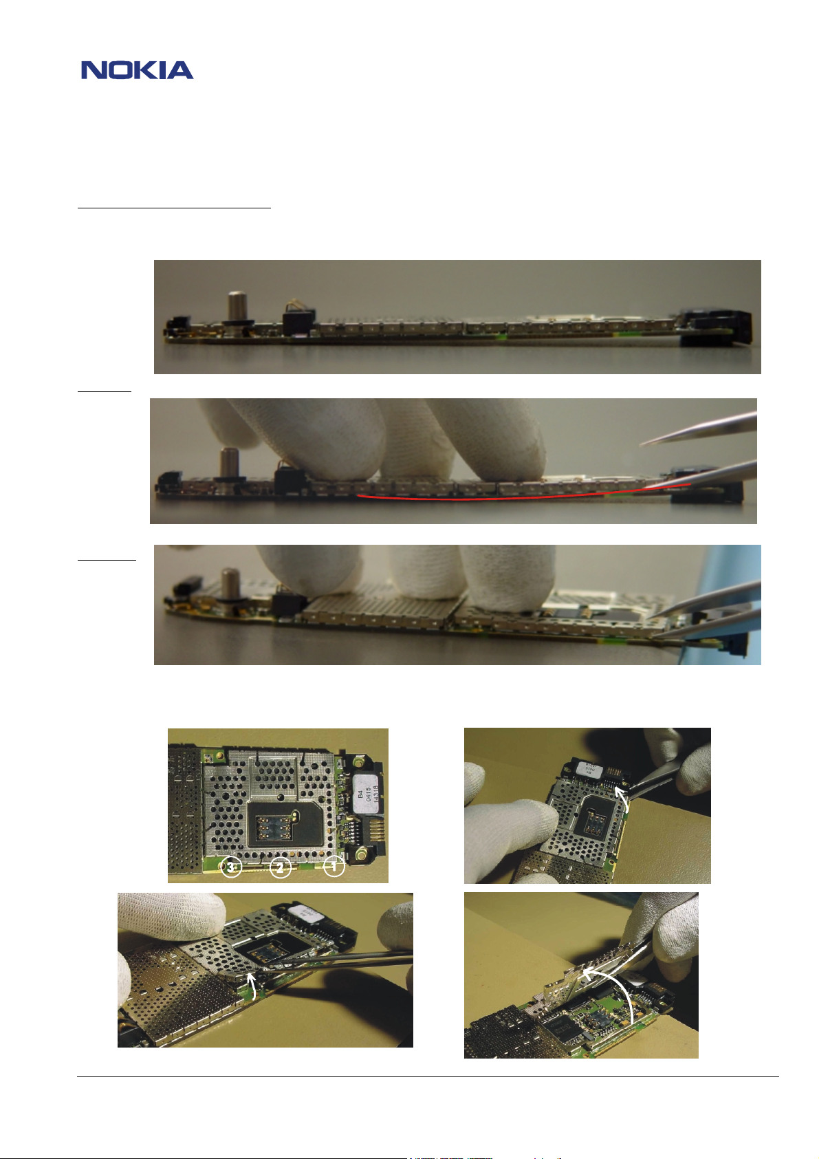
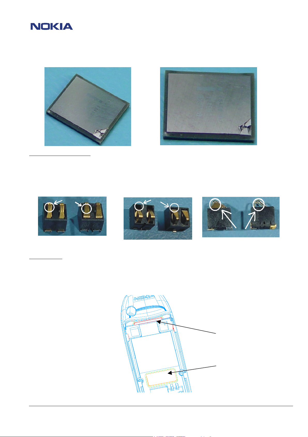
BB shield disassembly instructions
For disassembly it is important to lay the PWB on a plane underground so that the bottom connector is hanging free to prevent
bending of PWB and cracking of the connector´s solderings (See pictures below).
Wrong
Correct
When disassembling the BB shield be very careful because Flash D450 could be damaged (See pictures on next page).
Start by lifting and bending the lid with a tweezer at the marked points 1- 3 (see pictures below).
Do not use too much force on the frame because it could be damaged and the PWB also could be mechanical stressed.
© NMP 2002
Checked by:
SCCE Training Group
Approved by:
SCCE
Page 6
CONFIDENTIAL 6 (25)
NPE-4 6310/NPL-1 6310i Repairhints
Customer Care Europe & Africa Version 1.0 Approved
SCCE Training Group Date 15.08.2002
Example for a broken Flash D450:
Different battery connectors
There are two different battery connectors under the same part code 5400239 (See pictures below).
If it is nessesary to exchange the battery connector X101/ X102 take care that you use the same one.
The mixed replacement causes switch-off trouble.
Different surface, width and position of spring contacts:
Note! It is not allowed to use the battery connectors of NPE-3 (part code 5469069) because of smaller size.
Auto power off
The phone turns off, because the contact pads on the battery and the battery connectors are worn out and the phone has lost the
contact to the battery.
Assemble the Y- and Z-Pads, see picture below.
For more information see SB-010.
Difference
Difference
Difference
Difference
Battery Pad Y
Battery Pad Z
© NMP 2002
Checked by:
SCCE Training Group
Approved by:
SCCE
Page 7
CONFIDENTIAL 7 (25)
NPE-4 6310/NPL-1 6310i Repairhints
Customer Care Europe & Africa Version 1.0 Approved
SCCE Training Group Date 15.08.2002
Electrical faults
Totally dead
Check VBATIN=3.6 VDC at L260 (depends on workbench supply). If not ok, check X101, X102 battery connectors for mechanical
damages or cold solderings. Refer also to chapter “Additional Information/Different battery connectors”.
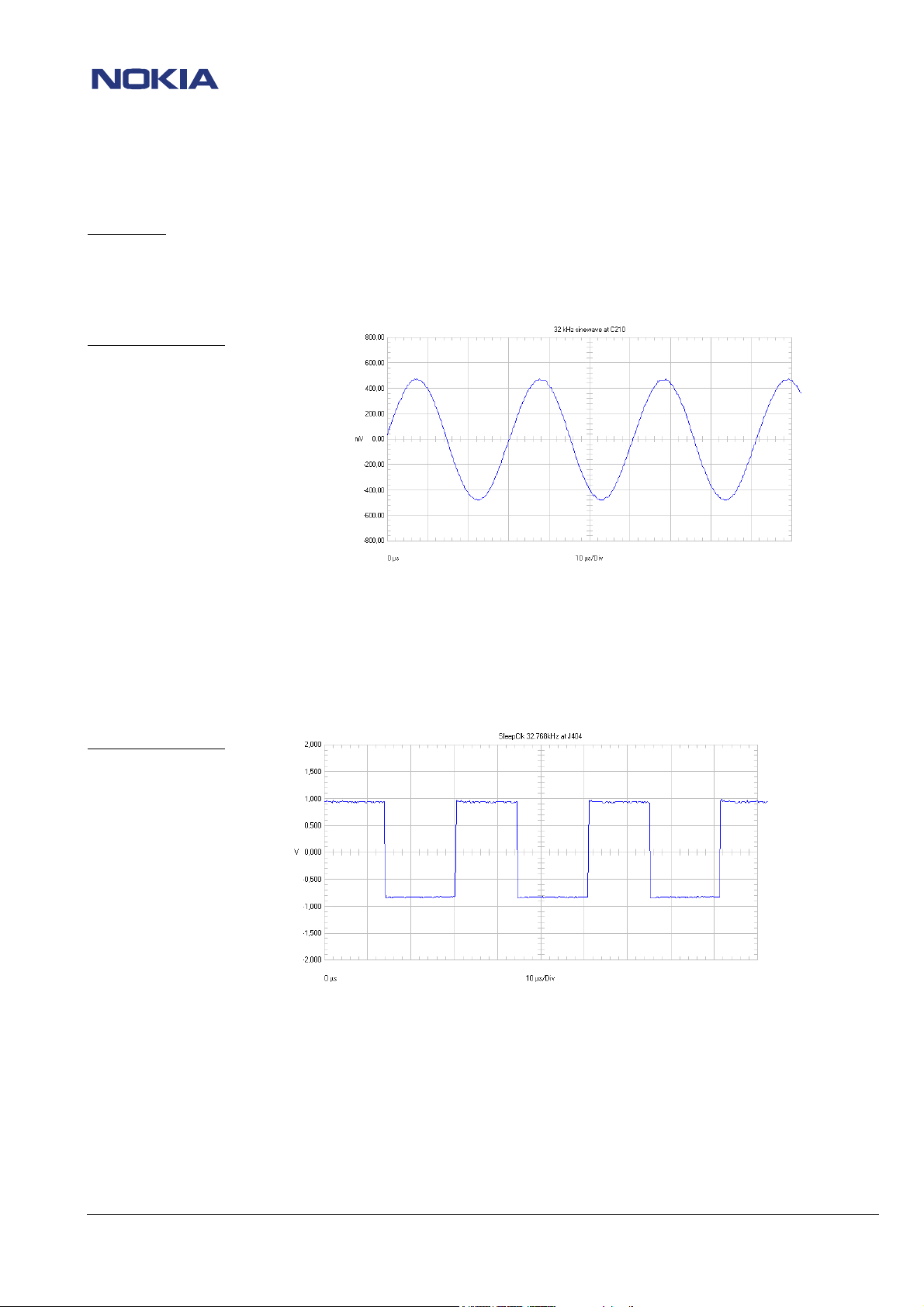
Check 32.768 kHz sinewave, Vpp = 800 mV at C209 (See picture below).
Oscilloscope settings:
Ampl: 200mV
Time/Div: 10µs/Div
AC/DC/GND: AC
If there is no signal, check B200 circuit for shorts or disconnection and change faulty components.
Check PWRONX at S300 pin 2/ 4: Key not pressed = 3.6 VDC (Depends on Workbench supply voltage)
Key pressed = 0 VDC
If not ok, check PWRONX-line from S300 to UPP D400 for shorts or disconnections.
Check SleepClk = 32.768 kHz, Vpp = 1.8 V square wave at J404. (See picture below)
Oscilloscope settings:
Ampl: 500mV
Time/Div: 10µs/Div
AC/DC/GND: AC
If not ok, check B200 circuit for shorts or disconnections.
Check VCORE = 1.8 VDC at C400. If not ok, check UEM D200
Check PURX = 1.8 VDC at V130 Pin 44. If not ok, check UEM D200
Check System Clk = 26 MHz, Vpp = 800 mV at C752 (See picture below)
© NMP 2002
Checked by:
SCCE Training Group
Approved by:
SCCE
Page 8

CONFIDENTIAL 8 (25)
NPE-4 6310/NPL-1 6310i Repairhints
Customer Care Europe & Africa Version 1.0 Approved
SCCE Training Group Date 15.08.2002
Oscilloscope settings:
Ampl: 500mV
Time/Div: 20ns/Div
AC/DC/GND: AC
If not ok, check 26 MHz G740 circuit. Refer also to chapter Drop calls
Check RFClk = 13 MHz, Vpp = 600 mV at C424. If not ok, refer to No service/ No RSSI.
Check VIO = 1.8 VDC at C450. If not ok, check VIO line to UEM D200 for shorts or disconnections and change faulty components.
If all above-mentioned signals are ok, try to flash the phone.
If the the flash update fails, the prommer will display a fault message (see picture below)
Check VPP at C454 = 1.8VDC
If VPP is not ok, UPP D400 is faulty. Change PWB, because UPP is not changeable.
Check VFLASH2 at C280 = 1.8VDC
If not ok, UEM D200 is faulty. Change PWB, as UEM is not changeable.
If both voltages are ok, try to flash the phone with repair jig MJS-40 and measure the VFLASH2 again. Now the voltage at C280
rises up to 2.8VDC.
If the voltage does not rise up to 2.8VDC, change PWB, as the UEM D200 is not changeable.
If all voltages are ok, check the Flash for mechanical damage (see also picture at chapter Additional
information/BB shield disassembly instructions/Example for a broken Flash D450).
Change Flash D450 in following cases when all other signals ok:
- Mechanical damages (See picture at Additional Information/Example for broken Flash D450)
- IMEI not rewriteable or SimLock Test fails
After changing the Flash D450, rewrite product code, HW-ID, IMEI and SIMlock settings.
If the fault persists, probably UEM D200 is faulty and not changeable. Change the PWB.
Note! Rewrite SIMlock and IMEI data by use of NOKIA SECURITY PASSWORD and tune the phone again, if the procedure
is permitted to you. (See General SB–037)
© NMP 2002
Checked by:
SCCE Training Group
Approved by:
SCCE
Page 9

CONFIDENTIAL 9 (25)
NPE-4 6310/NPL-1 6310i Repairhints
Customer Care Europe & Africa Version 1.0 Approved
SCCE Training Group Date 15.08.2002
Drop calls
Disassemble the NPE-4 and the RF- shield, then connect the PWB to the MJS-40 jig.
Insert a SIMcard and connect the coaxial cable to the tester (e.g. CMD/Wavetec). Now start a call.
If the call is established, check the analyzer display from tester (e.g. CMD/Wavetec) shows a frequency error.
If fault does not appear or appears intermittently only, press on 26MHz oscillator G740 with non-metallic item.
If the frequency error appears or increases in this case, probably the 26MHz circuit is faulty.
Open the Phoenix menu Testing/ RF controls and activate local mode RX GSM900
Check 26MHz +/- 100Hz between C752 and R752 with spectrum analyzer and active frequency counter (See picture below)
If the frequency drift is higher than +/ - 100Hz, check VR3 (VCC) = 2.8 VDC at R740.- If not ok, check UEM D200.
Check AFC (around 1.3 VDC) at G740. Check also if VR3 (VCC = 2.8 VDC) is ok with an Oscilloscope.- If not ok, check UEM D200
If both voltages are ok but the frequency drift is higher than +/ - 100Hz and the fault is getting stronger when pressing the top of
the 26MHz oscillator G740, change the faulty component.
No service
Set phone to local mode with Phoenix
Open menu Maintenance/Tuning/RX Calibration
Check RX calibration in GSM/PCN. If not ok, refer to chapter No Service/No RX
If RX calibration is ok, open menu Maintenance/Tuning/TX power
Check TX power in GSM/PCN. If not ok, refer to chapter No Service/No TX
If TX power is ok, insert Test-SIM and set phone to normal mode.
Start a Test call If not ok, make a SW update and try connecting again.
Note! Rewrite SIMlock and IMEI data by use of NOKIA SECURITY PASSWORD and make a SW-update again, if the
procedure is permitted to you. (See General SB–037)
If the connection is established, check with tester (e.g. CMD/Wavetec) if any errors appears on display (e.g. frequency error).
If a frequency error appears, refer to chapter Drop calls.
If the fault persists after SW update, rewrite IMEI and SIMLock settings.
© NMP 2002
Checked by:
SCCE Training Group
Approved by:
SCCE
Page 10

CONFIDENTIAL 10 (25)
NPE-4 6310/NPL-1 6310i Repairhints
Customer Care Europe & Africa Version 1.0 Approved
SCCE Training Group Date 15.08.2002
Flowchart – No service
No Service
Set phone with Phoenix
to Local Mode
Open menu
Maintenance/Tuning/RX
calibration
Check RX calibration
in
GSM/PCN
OK
Check TX power at menu
Maintenance/Tuning/TX power
OK
Insert a Test Sim,
set phone to normal
mode
and make a Test call
OK
Connection
established?
OK OK
Check
CMU/CMD if
any errors appear on display,
e.g.frequency
errors
OK
Phone is ok
nOK
nOK
nOK
nOK
Refer to chapter
No Service/No RX
Refer to chapter
No Service/No TX
Make a sw update and try
connecting again
Refer to chapter
Drop calls
If the fault persists,
rewrite IMEI/SIMLock
nOK
settings are not ok
© NMP 2002
Checked by:
SCCE Training Group
Approved by:
SCCE
Page 11

CONFIDENTIAL 11 (25)
NPE-4 6310/NPL-1 6310i Repairhints
Customer Care Europe & Africa Version 1.0 Approved
SCCE Training Group Date 15.08.2002
No Service →→→→ no RSSI
Set the RF generator to GSM 942.4 MHz at channel 37, RF level –55 dBm and also the phone to same frequency and channel.
Check RX I/Q signals at C721, C722 (See picture below)
Always measure in burst mode (with an oscilloscope in DC mode).
Oscilloscope settings:
Ampl: 200mV
Time/Div: 1ms/Div
AC/DC/GND: DC
If not ok, check 67.71 kHz at C714 (DtoS and Biquad filter).
Measurement points at C714 count from N600 Hagar side: At first pins (3/4)= DtoS I/Q;
and then pins (1/2)= Biquad (CM_F and CP_F I/Q).
All measurements made in Burst Mode (with an oscilloscope in DC mode).
DtoS
Biquad
Oscilloscope settings:
Ampl: 500mV
Time/Div: 200µs/Div
AC/DC/GND: DC
If the signal is not ok, check in GSM the RX signal 942.4 MHz at channel 37, RF level –55 dBm at L626.
If the signal is not ok, check in PCN the RX signal 1842.4 MHz at channel 700, RF level –55 dBm at L616
If both RX signals not ok, check RX lines from N600 Hagar to X802 antenna connector for shorts or
disconnections.
If the RX signals are ok, check System Clk = 26 MHz at C752 (See picture at chapter “Electrical faults”/ Totally dead)
If also the System Clk is ok, check following voltages:
Check VR3 = 2.8 VDC at C602.
Check VR4 = 2.8 VDC at C601
Check VR5 = 2.8 VDC at C604
Check VR6 (VBB) = 2.8 VDC at C605
Check VR1A (VCP) = 4.7 VDC (supply for control voltage VC for SHF oscillator) at C600
Check VR7 = 2.8 VDC at C299 (supply voltage VCC for SHF oscillator)
Check VREF01 and VREF02 = 1.35 VDC at R726
If one of the upper described voltages is not ok, check UEM D200.
If all voltages are ok, change N600 Hagar.
© NMP 2002
Checked by:
SCCE Training Group
Approved by:
SCCE
Page 12

CONFIDENTIAL 12 (25)
NPE-4 6310/NPL-1 6310i Repairhints
Customer Care Europe & Africa Version 1.0 Approved
SCCE Training Group Date 15.08.2002
Flowchart - No service →→→→ no RX
No Service /
No RSSI
Set Phone to RX-Burst-Mode.
Set RF Generator to Ch. 37,
RX-level -55 dBm
Set Spectrum Analyzer to
RX EGSM 942.4 MHz,
.
Check
RX I/Q-Signal 67.71 kHz
,Vpp=1.1V at C721 (set
oscilloscope to DC-Mode)
500 mV, Time base
1 ms.
OK
Check D200
UEM
nOK
Check RX-line to X102
antenna connector fo r
shorts or disconnection s
Check
PCN RX-Signal
1842.4 MHz, Ch. 700,
at L616
OK
Check G740 26 MHz
oscillator circuit
nOK
Check
Dtos 67.71 kHz
at C714.
nOK
nOK
nOK
VR3 = 2.8 VDC at C602; VR1A = 4.7 VDC
at C600; VR4 = 2.8 VDC at C601;
VR5 = 2.8 VDC at C604; VR6 = 2.8 VDC
at C605; VR7 =2.8 VDC at R630;
Check
RX-Signal 942.4 MHz,
at L626
OK
Check
Sys CLK 26 M Hz
Vpp = 800 mV at
C752
OK
Check
following voltages:
VREFRF01 & VREFRF02
= 1.35 V at R726
OK
Check
CP_F I/Q (BIQUAD)
67.71 kHz
at C714
nOK
Check
C714 for cold or
broken
solderings.
OK
Check
following voltages :
VR4 = 2.8 VDC at C601;
VR6 = 2.8 VDC
at C605
nOK
OK
nOK
nOK
OK
Change N600
Hagar
Change C714
Change N600
Hagar
Check D200
UEM
© NMP 2002
OK
Change N600
Hagar
Checked by:
SCCE Training Group
Approved by:
SCCE
Page 13

CONFIDENTIAL 13 (25)
NPE-4 6310/NPL-1 6310i Repairhints
Customer Care Europe & Africa Version 1.0 Approved
SCCE Training Group Date 15.08.2002
No service →→→→ no TX
Check EGSM TX signal at R656 / R657 (See picture below)
Set spectrum analyzer to TX EGSM 897.4 MHz, channel 37.
Set phone to TX mode, EGSM 897.4 MHz, channel 37 and power level 10.
If there is no signal measurable, check PCN TX signal at L662 (See picture below)
Set spectrum analyzer to TX PCN 1747.8 MHz, channel 700.
Set phone to TX mode, PCN 1747.8 MHz, channel 700 and power level 10.
If both TX signals ok, check EGSM/ PCN TX lines between Hagar N600 and antenna connector X802 for shorts or disconnections
If there is no TX signal measurable at L662, check TX I/Q at C764 and C766 on both sides of capacitors.
(See picture below)
Oscilloscope settings:
Ampl: 500mV
Time/Div: 1ms/Div
AC/DC/GND: DC
If the TX I/Q signal is not ok, check UEM D200
© NMP 2002
Checked by:
SCCE Training Group
Approved by:
SCCE
Page 14

CONFIDENTIAL 14 (25)
NPE-4 6310/NPL-1 6310i Repairhints
Customer Care Europe & Africa Version 1.0 Approved
SCCE Training Group Date 15.08.2002
Check TXC at C761, power level 19 and 5. (See picture below)
Oscilloscope settings:
Ampl: 500mV
Time/Div: 10ms/Div
AC/DC/GND: AC
Power level 19
If the TXC signals are not ok, check UEM D200
Check TXP signal at J760. (See picture below)
Oscilloscope settings:
Ampl: 500mV
Time/Div: 1ms/Div
AC/DC/GND: AC
If the TXP signal is not ok, check UPP D400.
Check System Clk = 26 MHz at C752 (See picture at chapter Electrical faults/ Totally dead)
If also the Sys Clk is ok, check following voltages:
Check VR3 = 2.8 VDC at C602 (supply voltage for 26 MHz oscillator G740).
Check VR4 = 2.8 VDC at C601
Check VR5 = 2.8 VDC at C604
Check VR6 (VBB) = 2.8 VDC at C605
Check VR1A (VCP) = 4.7 VDC at C600 (control voltage VC for SHF oscillator).
Check VR7 = 2.8 VDC at C299 (supply voltage VCC for SHF oscillator).
Check VREF01 and VREF02 = 1.35 VDC at R726
If one of the upper described voltages is not ok, check UEM D200.
If all voltages are ok, change Hagar N600.
Power level 5
© NMP 2002
Checked by:
SCCE Training Group
Approved by:
SCCE
Page 15

CONFIDENTIAL 15 (25)
NPE-4 6310/NPL-1 6310i Repairhints
Customer Care Europe & Africa Version 1.0 Approved
SCCE Training Group Date 15.08.2002
Flowchart - No service →→→→ no TX
No Service/
No TX EGSM/PCN
Set Phone to TX -Mode
EGSM 897.4 MHz,
Ch. 37, power level 10.
Set Spectrum Analyzer to
TX EGSM 897.4 M Hz, Ch.37
Check TX
EGSM 897,4 MHz
at R65 6.
nOK
OK
Check TX I/Q
67.71 kHz signal at
C764 and C766 at
both sides.
OK
Check
TXP VDC > 1.8 V
at C76 0 with
oscilloscope
OK
Set Phone to TX -Mode
PCN 1747.8 MHz,
Ch.700, power level 10.
Set Spectrum Analyzer to
PCN 1747.8 MHz, CH. 700
Check TX
PCN 1747.8 MHz
at L602.
nOK
OK
nOK
nOK
Check TX EGSM/PCN path from
Hagar to X802 antenna connector
for shorts or disconnections.
Probably N840 defect.
Check UEM D200
Check UPP D400
Check TXC
signal at C761
with oscilloscope.
OK
Check 26 MHz
at C752.
OK
Check the
following voltage s:
VR2 = 2.8 VDC at C294; VR3 = 2.8 VDC at
C602; VR4 = 2.8 VDC at C601;
VR5 = 2.8 VDC at C604; VR6 = 2.8 VDC at
C605; VR7 = 2.8 VDC at C299;
VrefRF01 & VrefRF02 = 1.35 VDC at R726;
VR1A = 4.7 V at R600
OK
Hagar N600
defect.
nOK
nOK
nOK
Check UEM D200
Check 26 MHz
circuit, especially
G740
Check UEM D200
© NMP 2002
Checked by:
SCCE Training Group
Approved by:
SCCE
Page 16

V
CONFIDENTIAL 16 (25)
NPE-4 6310/NPL-1 6310i Repairhints
Customer Care Europe & Africa Version 1.0 Approved
SCCE Training Group Date 15.08.2002
Display too dark/ too bright
When turning on the phone, the display LED´s V300 – V303
(See picture below) shine in different brightness.
This is caused by use of different LEDs. In this case change all LEDs and
assemble the right ones with spare part code 4864293.
Note! When changing the LEDs, first the RF frame has to be removed.
Be very careful when lifting the frame with hot air. A little drift beside
and some small components might be pushed away.
300-V303
© NMP 2002
Checked by:
SCCE Training Group
Approved by:
SCCE
Page 17

CONFIDENTIAL 17 (25)
NPE-4 6310/NPL-1 6310i Repairhints
Customer Care Europe & Africa Version 1.0 Approved
SCCE Training Group Date 15.08.2002
Tuning problems with Phoenix SW 3.72.002
Tuning problem with FPS-8
If the NPE-4 is connected to FPS-8 Flashbox via FBUS-cable, the reset does not work. When closing the energy management
calibration window, Phoenix tries to reset the phone. The NPE-4 goes in off state and does not start again automatically. In this
case the phone has to be switched on manually.
RX Channel Select Filter calibration all measurements = “0” at GSM1800
There is a misleading information in RX Channel Select Filter calibration at GSM1800. All values are “0” after tuning the “RX
Channel Select Filter calibration” under menu “Tuning/ RX Channel Select Filter calibration”. The shown information is wrong.
Tune the phone only in GSM900. These values are the same also for GSM1800.
For more information look at SB-026.
TX tuning problem
When starting TX tuning without connected coaxial cable to X802 antenna connector and going to power level 8 or higher, the
phone goes in reset state.
Everytime when tuning the phone first connect the coaxial cable and then start the tuning procedure.
SW faults
Totally dead
Phone jammed
No memory access/ hangs up
No service
If one of the above mentioned faults happens, first try to flash the phone with SW version 4.31 or newer.
If the fault persists refer to chapter Electrical faults/ totally dead
© NMP 2002
Checked by:
SCCE Training Group
Approved by:
SCCE
Page 18

CONFIDENTIAL 18 (25)
NPE-4 6310/NPL-1 6310i Repairhints
Customer Care Europe & Africa Version 1.0 Approved
SCCE Training Group Date 15.08.2002
Hookswitch problems
Sometimes not possible to release “incoming call”
No voice dial possible
When the headset HDC-9P is connected to the botton connector of NPE-4 and a call is coming in, often it is not possible to
release the call by pressing the hookswitch.
Often it is also not possible to initiate the voice call by pressing the hookswitch.
If one of the above mentioned problems occures, the changing of R175 can solve the problem.
Open the BB-shield and measure the resistor R175=100kΩΩΩΩ.
If R175=100kΩΩΩΩ, change the resistor to 15kΩΩΩΩ.
Note! Up to HW-ID 06.01 there is a 100kΩΩΩΩ resistor. From HW-ID 06.02 the value has changed to 15kΩΩΩΩ.
For more information also see SB 024
(See pictue below).
100kohm
15kohm
© NMP 2002
Checked by:
SCCE Training Group
Approved by:
SCCE
Page 19

CONFIDENTIAL 19 (25)
NPE-4 6310/NPL-1 6310i Repairhints
Customer Care Europe & Africa Version 1.0 Approved
SCCE Training Group Date 15.08.2002
NPL-1 6310i
No service
Drop calls
No TX 1800/1900
Insert Test Sim into phone and try to establish a connection at GSM900/1800 and 1900 with e.g. CMD/Wavetec.
If a connection is established try to make a call. Find out which TX band is faulty.
If a connection is possible in GSM900 only, refer to No GSM1800/1900 later on in this chapter.
Drop calls
If, in all GSM Bands, a connection is possible, but the bit error rate is to high and the connection is bad, set phone too local mode
and check TX spectrum at R805 (GSM900) and (See picture below)
If the spectrum is not ok, check following measurement points:
VIO = 1.8VDC at R630
VR1A = 4.7VDC at R623
VR2 = 2.8VDC at C622
VR3 = 2.8VDC at R610
VR4 = 2.8VDC at C296
VR5 = 2.8VDC at R628
VR7 = 2.8VDC at C299
TX I and Q at C715/C716 on both sides (See picture below)
Bad spectrum spectrum ok
© NMP 2002
Checked by:
SCCE Training Group
Approved by:
SCCE
Page 20

CONFIDENTIAL 20 (25)
NPE-4 6310/NPL-1 6310i Repairhints
Customer Care Europe & Africa Version 1.0 Approved
SCCE Training Group Date 15.08.2002
Oscilloscope settings:
Ampl: 500mV
Time/Div: 1ms/Div
AC/DC/GND: DC
If one of the four TX I/Q signals are missing or to low (TX IN, TX IP and TX QN, TX QP), check R713 on both sides.
If TX I/Q signals towards UEM D200 are not ok, UEM or PWB is faulty.
If one of the voltages is missing, probably UEM D200 is faulty.
If all signals towards RF-IC N601 are ok, change Mjoelner N601.
No TX 1800/1900
Check VAPC_DCS signal at R821 (See picture below)
Use Phoenix and open menu Maintenance/RF controls. Set phone to TX 1800 / Powerlevel 0 and/or 15
Oscilloscope settings:
Ampl: 50mV
Time/Div: 2ms/Div
AC/DC/GND: DC
If there is no signal measureable, check R821, R820 and C832 for cold or broken solderings and resolder or change if necessary. If
all three components are ok, change N601 Mjoelner.
Powerlevel 0
Powerlevel 15
© NMP 2002
Checked by:
SCCE Training Group
Approved by:
SCCE
Page 21

CONFIDENTIAL 21 (25)
NPE-4 6310/NPL-1 6310i Repairhints
Customer Care Europe & Africa Version 1.0 Approved
SCCE Training Group Date 15.08.2002
Flowchart No Service
No Service
Drop calls
No TX 1800/1900
Insert TestSim into phone and
establish a connection at all
GSM Bands with e.g.
CMD/Wavetec. Make a call and
find out, which Band is faulty
Call in
all GSM Bands
possible?
Set phone to Local
Mode with Phoenix
and check with HF
Probe TX spectrum at
R805 (GSM900) and
R819 (GSM1800/1900
- difficult to measure)
nOK
OK
Bit
error rate
ok?
GSM 1800/1900 not ok.
Set Phone to TX-Mode
nOK
GSM 1800 1747.8MHz,
Ch. 700, Powerlevel 15
VAPC_DCS signal
at R821 with
oscilloscope
and 0
Check
OK
Check N801
Power
Amplifier
Check cable
connection
between phone
CMD/Wavetec
OK
and e.g.
TX
Spectrum
ok?
nOK
nOK
OK
Tune TX I/Q and
TX power
TX
Spectrum
ok?
nOK
OK
Phone ok
UEM D200 faulty.
Change PWB
nOK
voltages: VIO=1.8VDC at R630
VR1A=4.7VDC at R623, VR2=2.8VDC at C622
VR3=2.8VDC at R610, VR4=2.8VDC at C296
VR5=2.8V at R628, VR7=2.8VDC at C299
TX I/Q at C715/C716 on both sides
Check
following signals and
All signals ok?
OK
Change N601
Mjoelner
© NMP 2002
Checked by:
SCCE Training Group
Approved by:
SCCE
Page 22

CONFIDENTIAL 22 (25)
NPE-4 6310/NPL-1 6310i Repairhints
Customer Care Europe & Africa Version 1.0 Approved
SCCE Training Group Date 15.08.2002
Keypad faulty
If one or more keys are not working, disassemble phone and check resistance = 0Ω between keys on same Colum and Row with
ohmmeter.
For example key 7 is not working
Check Row D2 keys “1”, “4”, “7”, “*” resistance between the one and the other keys= 0Ω
Check Colum D5 keys “End”, Down” 7”, “8”, “9” resistance between the one and the other keys = 0Ω
If between two keys the resistance is approximate MΩ, change PWB because of broken connection.
If all resistance = 0Ω, remove Z300 EMI-Filter and measure the connection between keypad and red
solderpads from EMI-Filter. If connection is not ok, change PWB, because of broken connection.
If connection is ok, check with ohmmeter the resistance between ground and blue marked solderpads
resistance around 2MΩ
If resistance is lower than 1MΩ or higher than 10MΩ, change PWB, because the UPP D400 is faulty and not
changeable.
:
marked
© NMP 2002
Checked by:
SCCE Training Group
Approved by:
SCCE
Page 23

CONFIDENTIAL 23 (25)
NPE-4 6310/NPL-1 6310i Repairhints
Customer Care Europe & Africa Version 1.0 Approved
SCCE Training Group Date 15.08.2002
BB Selftest explanation for NPE-4/NPL-1
3.1. ST_AUX_DA_LOOP_TEST
This function tests the connection of AuxDa and UemInt signals between UPP and UEM. UPP loops 70us high pulse via AuxDa line
to UEM and back to UPP via UemInt line. If there is no connection the result is ST_NO_SIGNAL. If everything is ok the result is
ST_OK
3.1.1. ST_EAR_DATA_LOOP_TEST:
This function tests the connection of EarData and MicData signals between UPP and UEM. If there is no connection the result is
ST_NO_SIGNAL. If there is short circuit the result is ST_SHORT_CIRCUIT. If everything is ok the result is ST_OK.
3.1.2. ST_IR_LOOP_TEST
This function tests the connection of IRTx and IRRx signals between UPP and UEM. UPP loops test signal via IRTx line to UEM and
back to UPP via IRRx line. If there is no connection the result is ST_NO_SIGNAL. If there is short circuit between IRTx and IRRx the
result is ST_SHORT_CIRCUIT. If everything is ok the result is ST_OK.
3.1.3. ST_KEYBOARD_STUCK_TEST:
This function tests to see if a key is stuck. If some key is stuck/pressed, it is re-tested ST_KBD_REPEAT times with ST_KBD_DELAY
interval. If key is still down result is ST_FAIL. If no key is stuck the result is ST_OK. If some key is stuck the result is ST_FAIL.
3.1.4. ST_MBUS_RX_TX_LOOP_TEST:
This function tests the connection of MBusTx and MBusRx signals between UPP and UEM. If everything is ok the result is ST_OK.
If there is no connection the result is ST_NO_SIGNAL.
3.1.5. ST_PPM_VALIDITY_TEST
This function checks the validity of PPM on flash.
3.1.6. ST_SIM_CLK_LOOP_TEST:
This function tests the connection of SimClk and SimIODa signals between UPP and UEM. This test also requires that SimIOCtrl
signal can be set to high state. (See also st_sim_io_ctrl_loop_test.) If everything is ok the result is ST_OK. If there is no
connection the result is ST_NO_SIGNAL. If there is short circuit the result is ST_SHORT_CIRCUIT.
3.1.7. ST_SIM_IO_CTRL_LOOP_TEST:
This function tests the connection of SimIOCtrl and SimIODa signals between UPP and UEM. This test also requires that SimClk
signal state can be switched. (See also st_sim_clk_loop_test.) If everything is ok the result is ST_OK. If there is no connection the
result is ST_NO_SIGNAL.
3.1.8. ST_SLEEP_X_LOOP_TEST:
This function tests the connection of SleepX and SleepClk signals between UPP and UEM. UEM_V2 or later required. If everything
is ok the result is ST_OK. If there is no connection the result is ST_NO_SIGNAL.
3.1.9. ST_TX_IDP_LOOP_TEST:
This function tests the connection of TxIdp and RxIdp signals between UPP and UEM. UEM_V2 or later required. If everything is ok
the result is ST_OK. If there is no connection the result is ST_NO_SIGNAL. If there is short circuit the result is ST_SHORT_CIRCUIT.
3.1.10. ST_TX_IQ_DP_LOOP_TEST:
This function tests the connection of TxQdp and RxQdp signals between UPP and UEM. UEM_V2 or later required. If everything is
ok the result is ST_OK. If there is no connection the result is ST_NO_SIGNAL. If there is short circuit the result is
ST_SHORT_CIRCUIT.
3.1.11. ST_BACKUP_BATT_TEST:
This function tests if the backup battery was ok during power-up. Ok means that there was enough power in the battery. If
backup battery is not ok the result is ST_FAIL. If backup battery is ok the result is ST_OK.
© NMP 2002
Checked by:
SCCE Training Group
Approved by:
SCCE
Page 24

CONFIDENTIAL 24 (25)
NPE-4 6310/NPL-1 6310i Repairhints
Customer Care Europe & Africa Version 1.0 Approved
SCCE Training Group Date 15.08.2002
3.1.12. ST_UPP_REGISTER_VER_TEST:
This function compares the ASIC version to the compilation flag. Major ASIC version in UPP version register is compared against
ASIC version compilation flag. If the version is correct the result is ST_OK. If the version is wrong the result is ST_FAIL.
3.1.13. ST_RF_CHIP_ID_TEST:
This is the product specific selftest. Each product makes its own implementation. This test checks wether the ID register on the RF
Chip can be read and that it contains reasonable values. Usually this is done by asking RF Chip ID from DSP. In a word, this tests
the RFBUS lines (data, clock, enable) between the UPP and RF part.
3.1.14. ST_WARRANTY_TEST:
This function tests the Warranty Information State. If WIS is not WT_INFO_STATE_DEF the result is ST_OK. If WIS is
WT_INFO_STATE_DEF the result is ST_FAIL.
3.1.15. ST_FLASH_CHECKSUM_TEST:
This function calculates the checksum over flash ROM areas and checksum is compared to precalculated checksum in flash
header. If checksums are the same the result is ST_OK. If checksums are not same the result is ST_FAIL.
3.1.16. ST_LCD_TEST:
This function tests the connection of LCD by checking voltage level of VLCD. If voltage level is ok the result is ST_OK. If voltage
level is not ok the result is ST_FAIL.
3.1.17. ST_IR_IF_TEST:
This function performs a self test on the IR device. The test checks that IR energy is looped back when the module is operating
normally.
3.1.18. ST_UEM_CBUS_IF_TEST:
This function tests that the connection to UEM via CBUS is working. First the value is written to UEM register and then it is read
back. The written and read values are compared with each other. If the values are the same, the result is ST_OK. If the values are
not same, the result is ST_FAIL. So basically this tests the CBUS lines (data, clock, enable) between UEM and UPP.
3.1.19. ST_PA_TEMP_TEST:
This function tests that PA temp line AD conversion is within reasonable limits. This means that the value is not at the bottom or
top end of the scale. First, several raw values of the temperature (PATEMP) are read. Then the average is calculated and compared
to the limits. If temperature is within the limits the result is ST_OK. If temperature is outside the limits the result is ST_FAIL. In a
word, this tests the PATEMP line between the UEM and RF.
3.1.20. ST_RADIO_TEST:
This function provides a method to turn on the radio and verify that the radio chip is present. If detection fails power will be
automaticelly turned off from the chip. If radio supply voltage VFLASH2 is missing or FMCtrlClk and FMCtrlDa lines are not
working the result is ST_FAIL. If the radio chip is present and working ok the result is ST_OK.
© NMP 2002
Checked by:
SCCE Training Group
Approved by:
SCCE
Page 25

CONFIDENTIAL 25 (25)
NPE-4 6310/NPL-1 6310i Repairhints
Customer Care Europe & Africa Version 1.0 Approved
SCCE Training Group Date 15.08.2002
CHANGE HISTORY
Originator Status Version Date Comment
TS Training
Group
TS Training
Group
TS Training
Group
TS Training
Group
Draft
Approved
Draft
Approved
0.1
1.0
1.1
2.0
17.04.2002
27.05.2002
09.08.2002
15.08.2002
First draft version for the repair group
Approved version
Draft version for the repair group
Approved version
© NMP 2002
Checked by:
SCCE Training Group
Approved by:
SCCE
 Loading...