

Page 1
NHM—2/5/6 Repairhints
Customer Care Europe, Middle East & Africa 3410 Version 4.0 Approved
SCCE Training Group Date 20.11.2002
CONFIDENTIAL 1 (44)
Repairhints
Service-Level 3 & 4
3310/3330/
3410
NHM-2/5/6
© NMP 2002
Checked by:
Customer Care E&A
Approved by:
SCCE Training Group
Page 2
NHM—2/5/6 Repairhints
Customer Care Europe, Middle East & Africa 3410 Version 4.0 Approved
SCCE Training Group Date 20.11.2002
CONFIDENTIAL 2 (44)
GENERAL
-How to use this document
Put the colored schematics behind this manual.
Now you are able to follow these specifications with graphical layouts and it is easier for you to find the
components and measuring points.
-Component characteristics:
Some components contain important data.
Several described steps are only practicable if you are able to reflash/ realign the phone and/or rewrite
IMEI/SIMlock in certain cases. Please pay attention to separate notes.
-Broken balls, µBGA
All replaceable µBGA-components must be renewed after removing.
Reflow with hot air fan is strictly forbidden!
Check soldering points, remove oxidated solderings (broken balls) carefully by enclosing few new solder
before placing new components.
µBGA must be soldered only with NMP approved µBGA-rework machines (e.g. Zevac/OK International).
Only use recommended fluxtype and an appropriate amount of it.
-PCB handling & cleaning
To avoid damages of PCB and/or components through electrostatic discharging, handle the module in
ESD-suitable cases only. Always wear ESD-bracelets, which must be connected to earth bonding point.
Do not make any loose wiring connections or do some other unqualified rework anywhere.
For cleaning only use appropriate materials, do not use scratching or rubbing tools.
Because of organic surface protection (OSP) cleaning must only be done with a lint-free cloth, which may
be moistened with DI-water. IPA or other solvent like ethanol should only be used to clean gold pads for
spring contacts without affecting the surrounding copper layers.
-Realign after repair
Characteristics of replacement parts are different.
To prevent additional faults after repair (eg. low standby time, loosing network etc.) it is necessary to retune
phone values after repair. But never try to cover a fault by tuning.
© NMP 2002
Checked by:
Customer Care E&A
Approved by:
SCCE Training Group
Page 3
CONFIDENTIAL 3 (44)
NHM—2/5/6 Repairhints
Customer Care Europe, Middle East & Africa 3410 Version 4.0 Approved
SCCE Training Group Date 20.11.2002
INTRODUCTION
IMPORTANT:
This document is intended for use by authorized NOKIA Service Centers only.
The purpose of this document is to provide some further service information for NOKIA 3310 / 3330/3410 phones.
It contains a lot of collected tips and hints to find failures and repair solutions easily.
It also will give support to the inexperienced technicians.
Saving process time and improving the repair quality is the aim of using this document.
We have built it up based on fault symptoms (listed in "Contents") followed by detailed description for further analysis.
It is to be used additionally to the service manual and other service information, e.g. Service Bulletins.
For that reason it does not contain any circuit descriptions or schematics.
All measurements are made by using following equipment:
Nokia repair SW : WinTesla Version 6.46/15.04.2002
DLL version : 311.15.00 / 26.06.2002
Nokia module jig : MJS -19
Digital multimeter : Fluke 73
Oscilloscope : Hitachi V-1565; Fluke PM 3380A/B
Spectrum Analyzer : Advantest R3161 with an analogue probe
RF-Generator / : Rohde & Schwarz CMU 200
GSM Tester
While every endeavour has been made to ensure the accuracy of this document, some errors may exist. If the reader finds any
errors, NOKIA should be notified in writing, using following procedure:
Please state:
Title of the Document + Issue Number/Date of publication.
Page(s) and/or Figure(s) in error.
Please send to: Nokia GmbH
SCCE Training Group
Customer Care E&A
Meesmannstr.103
D-44807 Bochum / Germany
Email: training.sace@nokia.com
Copyright © Nokia Mobile Phones.
This material, including documentation and any related computer programs, is protected by copyright, controlled by Nokia Mobile
Phones. All rights are reserved. Copying, including reproducing, modifying, storing, adapting or translating, any or all of this
material requires the prior written consent of Nokia Mobile Phones. This material also contains confidential information, which
may not be disclosed to others without the prior written consent of Nokia Mobile Phones.
© NMP 2002
Checked by:
Customer Care E&A
Approved by:
SCCE Training Group
Page 4
CONFIDENTIAL 4 (44)
NHM—2/5/6 Repairhints
Customer Care Europe, Middle East & Africa 3410 Version 4.0 Approved
SCCE Training Group Date 20.11.2002
Contents
PREFACE 2
General 2
Introduction 3
List of flowcharts 6
List of figures 6
Important Information 7
AM Suppression tuning 8
CHAPTER 1 HW – CHANGES 11
Difficulties when removing B-Cover (SB13 / NHM-5) 11
Intermittent switch-off problem (SB 28 / NHM-5, SB 7 / NHM 6) 11
Correct component replacement in UB4_ 10 or later of NHM-5 (SB053) and NHM-6 (SB31) 12
HW Change description Overview of NHM-2/6 13
CHAPTER 2 CHANGING OF D301 14
Step by step description of changing the FLASH/EEPROM –combination D301 14-16
CHAPTER 3 PHONE DOES NOT SWITCH ON 17-19
CHAPTER 4 FLASH UPDATE NOT POSSIBLE 20
Failure message ”MCU boot failure,serial clock-/data line failure” 21
Failure message ”Algorithm code fail / alias ID missing” 21
Failure message ”External RAM failure” 21
CHAPTER 5 PHONE SWITCHES OFF INTERMITTENT 22
CHAPTER 6 LOW STANDBY / OPERATION MODE TIME 23
Low standby / operation time 23-24
Off state current fail 24
Sleep mode current fail 24
CHAPTER 7 NOT CHARGING 25
Not charging 26
Nothing happens if charger is connected 26
Display message “Not charging” 26
Display message “Reconnect charger”
© NMP 2002
Checked by:
Customer Care E&A
Approved by:
SCCE Training Group
Page 5
CONFIDENTIAL 5 (44)
NHM—2/5/6 Repairhints
Customer Care Europe, Middle East & Africa 3410 Version 4.0 Approved
SCCE Training Group Date 20.11.2002
CHAPTER 8 CONTACT SERVICE 27
MCU ROM Checksum failed 27
CCONT Interface failed 27
COBBA parallel/serial failed 27
DSP Alive test failed 27
EEPROM sec/tune checksum failed 27
CHAPTER 9 SIMCARD FAULTS 28
Display message “Insert SIMcard” 29
Display message ”SIMcard not accepted” 29
CHAPTER 10 INTERNAL AUDIO FAULTS 30
Speaker faulty 30
Microphone does not work 30
CHAPTER 11 USER INTERFACE FAULTY 31
Display failure 31
Keypad malfunction 31
Backlight failure 31
Vibra failure 32
Buzzer failure 32
Clock time problems 32
CHAPTER 12 NO SERVICE 33
No or too low TX power GSM 900 33-37
No or too low TX power GSM 1800 37
Faulty spectrum 38
No RX-calibration GSM 900 possible 39-42
No RX-calibration GSM 1800 possible 42
Poor service or no network coverage, C508 faulty 43
CHAPTER 13 CHANGE HISTORY 44
© NMP 2002
Checked by:
Customer Care E&A
Approved by:
SCCE Training Group
Page 6
CONFIDENTIAL 6 (44)
NHM—2/5/6 Repairhints
Customer Care Europe, Middle East & Africa 3410 Version 4.0 Approved
SCCE Training Group Date 20.11.2002
List of flowcharts
Flowchart 3-1 Phone does not switch on Chapter 3 17
Flowchart 4-1 Flash update not possible Chapter 4 20
Flowchart 6-1 Low standby/Operation mode time Chapter 6 23
Flowchart 7-1 Not charging Chapter 7 25
Flowchart 9-1 SIMcard faults Chapter 9 28
Flowchart 10-1 Internal audio faults Chapter 10 30
Flowchart 12-1 No service (no TX) Chapter 12 33
Flowchart 12-2 No Rx calibration GSM 900 possible “ 39
List of figures
Figure 1-1 D-Cover NHM-5 (the pin who is cut) Chapter 1 11
Figure 2-1 “Phone Identity Information” window in WinTesla Chapter 2 14
Figure 2-2 “Flash Menu Selection” window in WinTesla “ 14
Figure 2-3 “Flash Phone” window in WinTesla “ 15
Figure 2-4 Message after proceed “Flash Phone” window in WinTesla “ 15
Figure 2-5 “Default Factory values” window in WinTesla “ 16
Figure 2-6 Message after set ”Full Factory” on “Default Factory values” window “ 16
Figure 2-7 “Production Data Edit” window in WinTesla “ 16
Figure 3-1 32.768 kHz at C220 Chapter 3 18
Figure 3-2 13 MHz reference clock at C303 “ 18
Figure 3-3 26 MHz reference clock at G502 “ 19
Figure 3-4 13 MHz system clock at C559 “ 19
Figure 8-1 COBBACLK at J317 Chapter 8 27
Figure 9-1 SIMcard signal (5 Vpp) at the SIMcard pogo pins of the service jig Chapter 9 29
Figure 10-1 Bended connector on display assy Chapter 10 31
Figure 11-1 Vibra signal at N400 pin 16 Chapter 11 32
Figure 12-1 26 MHz at C546 Chapter 12 34
Figure 12-2 TXIQ-signals at R541/548 “ 34
Figure 12-3 13 MHz COBBACLK at J317 “ 34
Figure 12-4 897.6 MHz TX-spectrum at L514 “ 35
Figure 12-5 SCLK at R301 “ 35
Figure 12-6 SENA at R301 “ 35
Figure 12-7 SDATA at R300 “ 35
Figure 12-8 TXC at C542 “ 36
Figure 12-9 TXP at J503 “ 36
Figure 12-10 HAGARReset at C540 “ 36
Figure 12-11 SHF-signal (3590.4 MHz) at T502 pin 3/4 “ 36
Figure 12-12 Vapc at C565 “ 37
Figure 12-13 Normal spectrum (1747.8 MHz) “ 38
Figure 12-14 Spectrum with broken solderings under CCONT (1747.8 MHz) “ 38
Figure 12-15 Spectrum of faulty COBBA (1747.8 MHz) “ 38
Figure 12-16 Spectrum of faulty oscillator G500 “ 38
Figure 12-17 RX-signal 942.6 MHz at C545 “ 40
Figure 12-18 RX-signal 942.6 MHz at C534 “ 40
Figure 12-19 1.1 Vpp at base of V501 “ 40
Figure 12-20 2.6 Vpp at collector of V501 “ 40
Figure 12-21 67.708 kHz at pads of C512 “ 41
Figure 12-22 SHF-signal (3770.4 MHz) at T502 “ 41
Figure 12-23 67.708 kHz at R500 “ 41
Figure 12-24 67.708 kHz at R504 “ 42
Figure 12-25 “AFC information” windows in WinTesla 43
Figure 12-26 67.708 kHz at R504 with faulty C508 in comparison to “Figure 12-23” 43
Figure 12-27 67.708 kHz at R500 with faulty C508 in comparison to “Figure 12-24” 43
© NMP 2002
Checked by:
Customer Care E&A
Approved by:
SCCE Training Group
Page 7
CONFIDENTIAL 7 (44)
NHM—2/5/6 Repairhints
Customer Care Europe, Middle East & Africa 3410 Version 4.0 Approved
SCCE Training Group Date 20.11.2002
IMPORTANT INFORMATION
Changing of EEPROM D301
If it is necessary to change D301, take a look at chapter 2 on page 14 “Changing of D301” how to proceed.
Furthermore never change D301 if you have no permission to rewrite IMEI – otherwise all phone data will be lost!
To avoid further problems send the phone to a higher-level NOKIA Service Center.
Changing of COBBA N800
If it is necessary to change COBBA, you have to rewrite IMEI & SIMlock data and flash the phone!
Also RX/TX-values must be realigned.
Changing of CCONT N700
If it is necessary to change CCONT, you have to realign A/D values.
Changing components in RF-part
If it is necessary to change any main component in RF-part (IC´s, oscillators, filters…) you have to realign all RX/TX values.
In case of problems to tune RF-values of GSM1800 band, check in WinTesla Configure/Options if automatic rescan function
is activated for the phone. If selected, the band will change to GSM1800 but due to the rescan the phone changes back to
GSM900. To solve the problem deactivate the automatic rescan function if necessary.
© NMP 2002
Checked by:
Customer Care E&A
Approved by:
SCCE Training Group
Page 8
CONFIDENTIAL 8 (44)
NHM—2/5/6 Repairhints
Customer Care Europe, Middle East & Africa 3410 Version 4.0 Approved
SCCE Training Group Date 20.11.2002
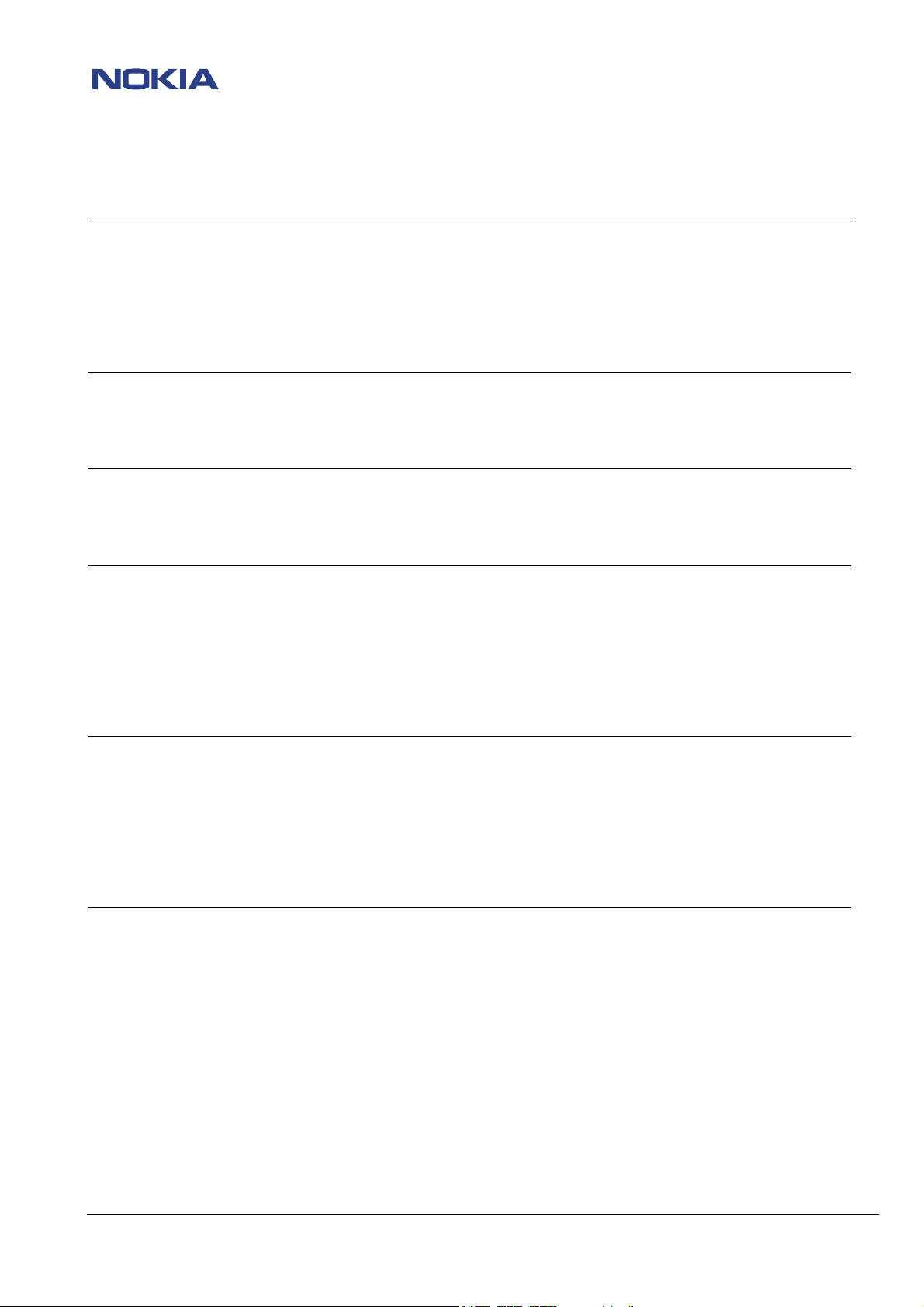
AM-suppression tuning in NHM-2/5/6
Due to a software failure in the latest NHM-2/5/6 DLL 311.15.00 it is necessary to run AM-suppression tuning in a special way,
as described in the following pages. In case you do not use this procedure the AM-suppression tuning values will not be saved and
WinTesla will not recognize the new values. So no warning message will be performed.
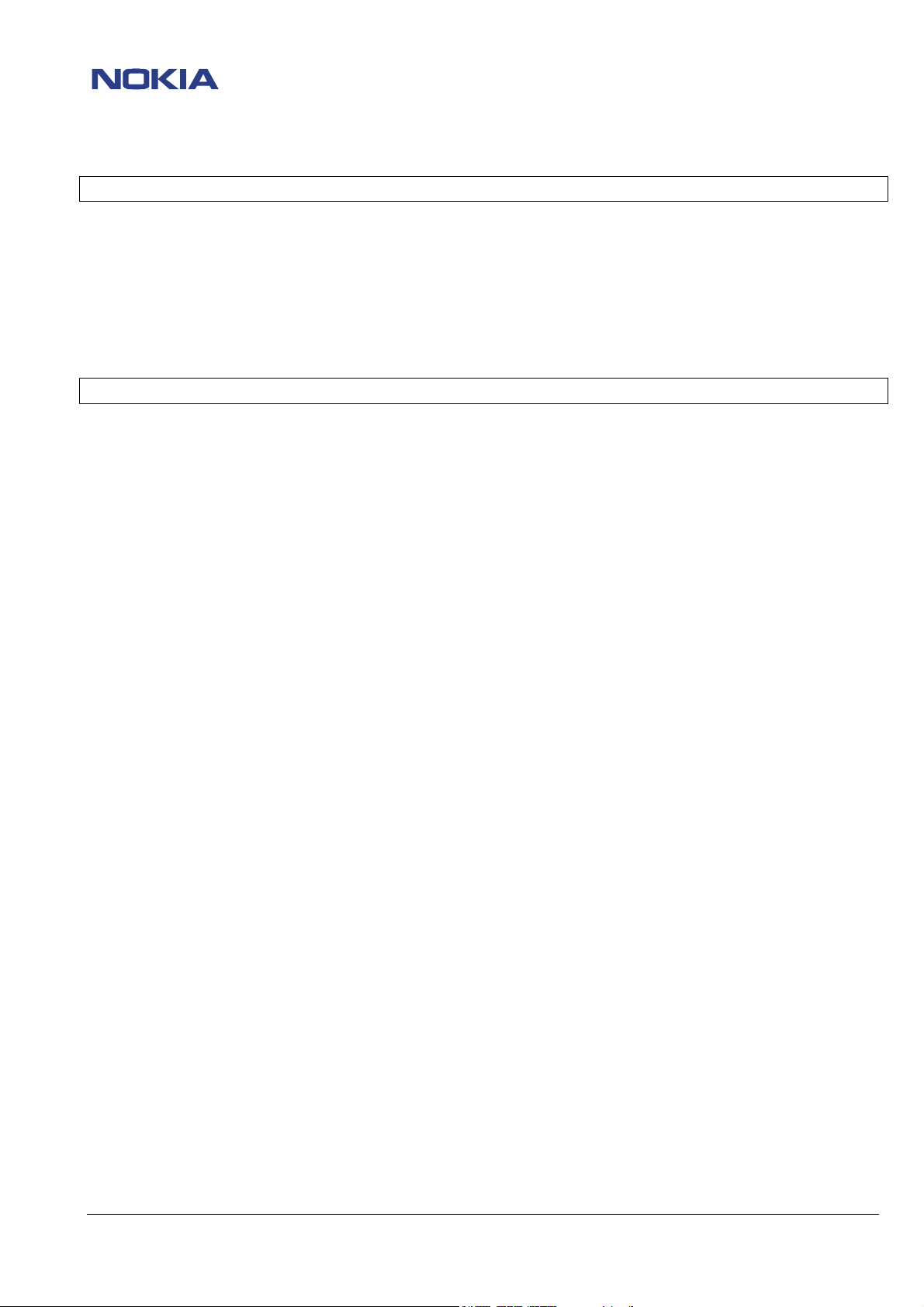
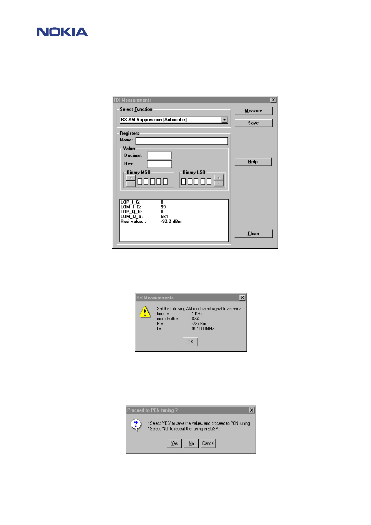
In the first step you have to activate AM-suppression tuning as usual (Tuning/AM Suppression…):
Click on the “Measure” button to get the next window, which shows the signal values you have to adjust, then click “OK”.
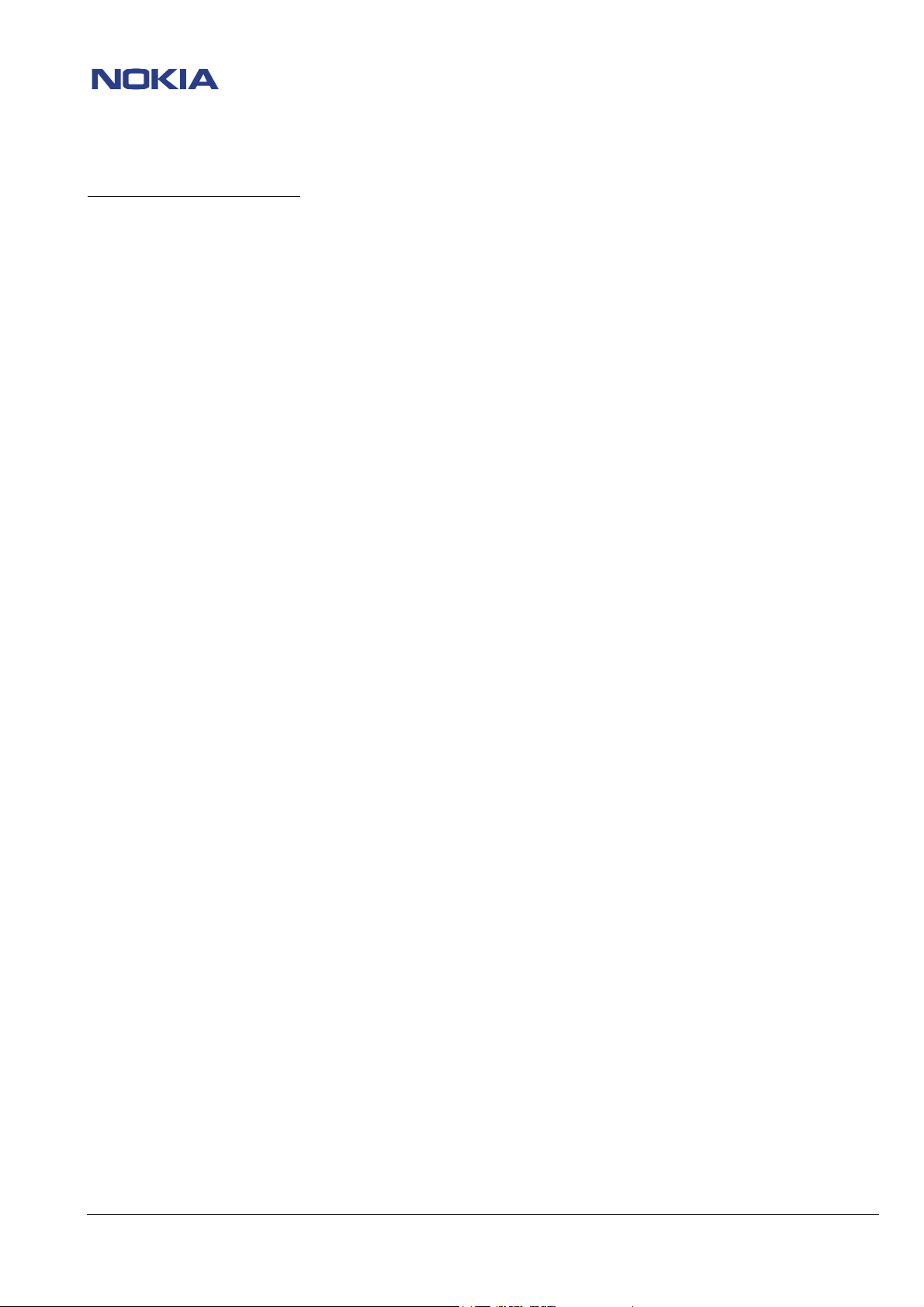
After correct AM-suppression tuning in EGSM900 (RSSI-level shown in the measurement window is < -86dBm) you get the
message to proceed the tuning in PCN. At this point do not press “YES” as, differently from the message box, the tuning values
will not be saved by choosing this button.
Click the button “Cancel” so that only the window shown on next page is performed on the screen.
© NMP 2002
Checked by:
Customer Care E&A
Approved by:
SCCE Training Group
Page 9
CONFIDENTIAL 9 (44)
NHM—2/5/6 Repairhints
Customer Care Europe, Middle East & Africa 3410 Version 4.0 Approved
SCCE Training Group Date 20.11.2002
To save the tuning values you have to click the “Save” button in this window.
Afterwards start the tuning procedure again by pressing the “Measure” button, because tuning in PCN yet must be done.
Next appearing window is shown below. Press “OK” (it is not necessary to choose correct signal values).
After having done AM-suppression tuning in EGSM900 a second time, press the “Yes” button.
As effect the tuning values of EGSM900 will not be stored (but these tuning values have been stored before).
You will be shown the message box as on next page so that you can continue tuning in PCN band.
© NMP 2002
Checked by:
Customer Care E&A
Approved by:
SCCE Training Group
Page 10
CONFIDENTIAL 10 (44)
NHM—2/5/6 Repairhints
Customer Care Europe, Middle East & Africa 3410 Version 4.0 Approved
SCCE Training Group Date 20.11.2002
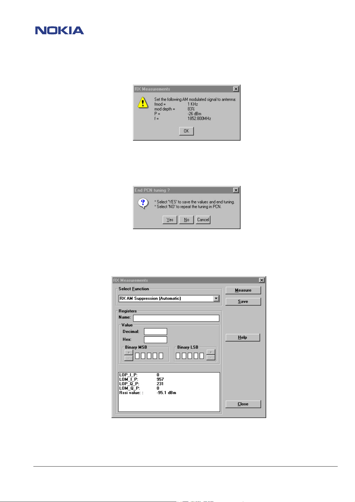
Set generator to the signal values mentioned in the control box. Then press the “OK” button.
To save the tuning values of AM-suppression in PCN band, do not use the “Yes” button. As in the case of EGSM900 choose the
“Cancel” button and click the “Save” button in the remaining window. RSSI-level in PCN tuning must be < -90dBm!
Now AM-suppression has been performed in both EGSM and PCN and you can leave the tuning by choosing “Close”.
© NMP 2002
Checked by:
Customer Care E&A
Approved by:
SCCE Training Group
Page 11
CONFIDENTIAL 11 (44)
NHM—2/5/6 Repairhints
Customer Care Europe, Middle East & Africa 3410 Version 4.0 Approved
SCCE Training Group Date 20.11.2002
CHAPTER 1: HW-CHANGES
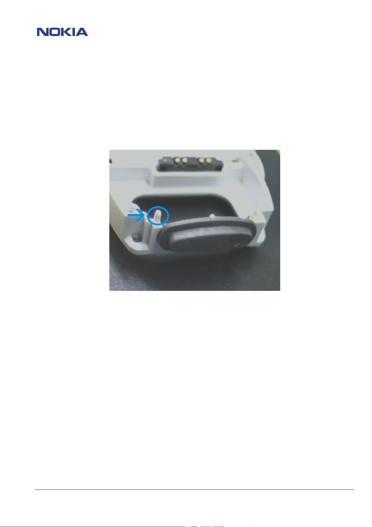
Difficulties when removing B-Cover (SB13 / NHM-5)
Cut away the guiding pin of the D-Cover (see Figure 1-1), if customer critisizes bad removal of B-Cover.
After this procedure it is necessary to assemble the phone with a torque screwdriver prepared for 30Ncm!
Figure 1-1
Intermittent switch - off problem (SB17 / NHM-2, SB 28 & 55 / NHM-5, SB 7 / NHM-6)
The change of R301 from 2x 2.2 k? to 2x100 ? because of “Intermittet switches off” not needed anymore since HW 0813 on
UP4IV, 0814 on UD4, 0815 on UG4 (NHM-5; SB 55), HW 0817 on UW4, 0818 on UW4II and 0819 on UX4 (NHM-6; SB 32) as in
the new HW version this change is already done. The change of R301 should be a solution in earlier HW versions only.
All NHM-2 HW versions have the correct value implemented already in production (SB – 017).
“Intermittet switches off” could be caused also by old ST flash, i.e. from before Week 02/2001.
Therefore it is recommended to use newer ST Flash IC.
Note that SB 28 & 55 replaces the SB 12. Do not use this procedure anymore!
© NMP 2002
Checked by:
Customer Care E&A
Approved by:
SCCE Training Group
Page 12
CONFIDENTIAL 12 (44)
NHM—2/5/6 Repairhints
Customer Care Europe, Middle East & Africa 3410 Version 4.0 Approved
SCCE Training Group Date 20.11.2002
Correct component replacement in UB4_ 10 or later of NHM-5 (SB053) and NHM-6 (SB31)
If changing the power amplifier (N502) & antenna switches (Z502) is necessary, it is recommended to replace with the same type
as the removed one.
The information in tables “PA vendor depent RF discrete component mount” and “Ant.sw./diplexer depent RF discrete components
mounts” in NHM-5/6 Service Manual must be followed if there is a really essential reason to use different type of power
amplifier or antenna switch as replacement
Only the following combinations of power amplifier and antenna are allowed for NHM-5/6:
Power Amplifier Antenna Switch
Hitachi (4350259) Murata (4550131)
Phillips (4350269) Matushita (4550201)
RFMD (4350277)
NHM-5
Power Amplifier Antenna Switch
Hitachi (4350259) Murata (4550131)
Phillips (4350269) Murata (4550131)
Matushita (4550201)
NHM-6
Note:
- After changing Power Amplifier, TX Power Tuning has to be carrying out.
- After changing Antenna Switch, Tx Power Tuning and RX Calibrations have to be carrying out.
After the Power Amplifier replacements, additional it should be checked in which constellation R311 and R312 were assembled
(marked “X”).
If necessary, adjust the resistors in the corresponding order to the type of PA.
Use for it the table below (PA vendor detection) as reference. (NHM-5; SB 25)
This is important because of the differences between the three power amplifier versions in use.
In UP4 Hitachi PA has been used while UD4 includes Philips PA and UG4 uses RFMD power amplifier.
Last mentioned is available as spare part meanwhile.
For PCB version up to Version 09 PCB version 10 and later
PA vendor detection
PA vendor Part. No. R312 (PA_vendor2) R311 (PA_vendor1)
RFMD 435X231
Phillips 435X194
Hitachi 4350259
Mounted
Mounted
PA vendor detection
PA vendor Part. No. R312 (PA_vendor2) R311 (PA_vendor1)
RFMD 435X231
Phillips 435X194
Hitachi 4350259
Mounted Mounted
Mounted
Mounted
© NMP 2002
Checked by:
Customer Care E&A
Approved by:
SCCE Training Group
Page 13
SCLK)
CONFIDENTIAL 13 (44)
NHM—2/5/6 Repairhints
Customer Care Europe, Middle East & Africa 3410 Version 4.0 Approved
SCCE Training Group Date 20.11.2002
HW Change description Overview of NHM-2/6
Hagar GSM1800 Output
(UX4)
match
UB4_11 PCB
Hagar v5
Cobba ST optical shrink (Note 4)
UB4_12 PCB
X
X
X X
X X X
X X X X 10.24
X X
X X X X X 10.26
X
X
X
X X X X 10.25
X X X
X
X X X X 10.28
X X X X
X
X
X
Cobba TI A07 (Note 4)
Part list
UW4 UB4_10 X
UW4 UB4_10 X
UW4 UB4_11 X
UW4 UB4_11 X
UW4 UB4_11 X
UW4 UB4_12 X
UW4 UB4_12 X
UX4 UB4_10
UX4 UB4_10
UX4 UB4_10
UX4 UB4_10
UX4 UB4_11
UX4 UB4_11
UX4 UB4_11
UX4 UB4_12
UX4 UB4_12
UW4II UB4_10 X
UW4II UB4_10 X
UW4II UB4_10 X
UW4II UB4_11 X
UW4II UB4_11 X
UW4II UB4_11 X
UW4II UB4_11 X
UW4II UB4_11 X
UW4II UB4_12 X
UW4II UB4_12 X
UW4II UB4_12 X
UW5 UB4_12 X
UW5 UB4_12 X
UW5 UB4_12 X
UW5 UB4_12 X
PCB version
Hitachi PA
Philips PA
RFMD PA
X
X
X
X
X
X
X
X
X
Antenna switch Matsushita
Antenna switch MURATA
X
X
X
X
X
X
X
X X
X X
X X
X X
X X
X X
X X
X X
X X
X X
X X
X
X X
X
X
X X
X X
X X
X X
X X
X
X
X
X
GSM TX Out match New
MAD2WD1-Hagar
s
VCO 4.0GHz FDK
VCO 4.0GHz Matsushita
VCTCXO NDK
VCTCXO Toyocom
TX SAW filter Epcos (Note 3)
TX SAW filter Panasonic (Note 3)
X X
X X
X X
X X
X X
X X
X X
X
X
X
X X
X X
X X
X X
X
X
X
X
X
X
X
X
X
X
X
X
X
X
X
X
X
X
X
X
X
X
X
X
X
X
X
X
X
X
X
Cobba TI A12 (Note 4)
X
X X
X X
X X
X X
X X
X X
X X
X X
X
X
X
X
X
X X X X X
X X X X X
X X X X X
X X X X
X X X X
X X X X
X
X X
X X X
X X X
X X X
X X
X X X
X
X X
X X
X X X
X X X
X X
X X X
X X X
X X X
Resistor'
(UW4 &
UW4II)
08.06
X
X
X X
X X X
X X X X
X
X
HW id - App. & Fixed
08.17
09.03
09.15
09.23
10.03
08.07
08.11
08.19
08.23
09.05
09.07
09.25
10.05
08.09
08.18
08.21
09.04
09.09
09.10
09.11
09.24
10.04
10.10
10.07
10.11
10.35
© NMP 2002
Checked by:
Customer Care E&A
Approved by:
SCCE Training Group
Page 14
CONFIDENTIAL 14 (44)
NHM—2/5/6 Repairhints
Customer Care Europe, Middle East & Africa 3410 Version 4.0 Approved
SCCE Training Group Date 20.11.2002
CHAPTER 2: CHANGING OF D301
This chapter describes step by step how to change FLASH/EEPROM-combination D301 in NHM-2/5/6 phones:
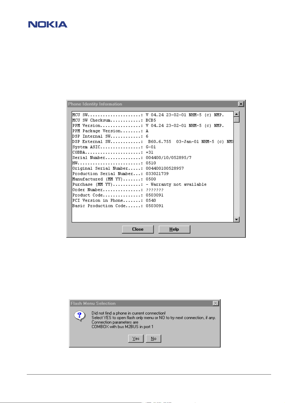
If you want to change D301 the first you always have to do is a backup of the phone identity information.
Therefore use WinTesla. Under “View” open the window “Phone Information”:
Figure 2-1
If you have no possibility to save this data (e.g. phone does not switch on because of defect D301), it is necessary to give the
phone a new identity!
Having saved the phone identity information, you can now remove D301 and resolder the spare part – always use approved µBGA
rework machine for changing any µBGA!
Because of the empty Flash the phone will not switch on, after changing D301. So the next action is to make a SW-update.
Start WinTesla and choose Product / Open / NHM-5 and press ok. Now you will receive the following message:
Figure 2-2
If you select Yes, WinTesla will start and you can choose Dealer / Flash Phone, and the window shown on the next page
appeares:
© NMP 2002
Checked by:
Customer Care E&A
Approved by:
SCCE Training Group
Page 15

CONFIDENTIAL 15 (44)
NHM—2/5/6 Repairhints
Customer Care Europe, Middle East & Africa 3410 Version 4.0 Approved
SCCE Training Group Date 20.11.2002
Figure 2-3
Now by pressing on the squares with the three dots you have to choose a MCU Image file and PPM file for your phone.
At this point it is not necessary to choose the right PPM file, because this SW-update is used only to make it possible to power
the phone on.
After selecting the two files you have to press the Flash-button to start the SW-update. Next message will be the following:
Figure 2-4
Select Yes and the SW-update will start. If your phone has no fault and the new FLASH/EEPROM was well soldered, you will get
order to Restore Default User Settings – press ok. After that you will get message, that flashing completed: press ok.
Now close the Flash Phone window by pushing the Close button.
© NMP 2002
Checked by:
Customer Care E&A
Approved by:
SCCE Training Group
Page 16

CONFIDENTIAL 16 (44)
NHM—2/5/6 Repairhints
Customer Care Europe, Middle East & Africa 3410 Version 4.0 Approved
SCCE Training Group Date 20.11.2002
As the next step open Software / Set Factory Values, choose Full factory and press Set:
Figure 2-5
You receive following message:
Figure 2-6
After pressing Yes you will get order to Restore Default User Settings – press ok. Now you can close the window shown on the
top of this page by pressing Cancel.
In the next step you have to open Software / Production Data Edit:
Figure 2-7
Rewrite product code and HW version out of your saved phone data into this window and press Save.
After this procedure you have to write back IMEI / SIMlock data and run SW-update once more. This time you have to choose
the correct flash file matching to your product code! Close the windows, which ask you to save user data to file by pressing No
and Restore Default User Settings by pressing ok after flashing.
Remember to retune RX/TX values and run energy management calibration, as all tuning data is lost after changing D301!
© NMP 2002
Checked by:
Customer Care E&A
Approved by:
SCCE Training Group
Page 17

CONFIDENTIAL 17 (44)
NHM—2/5/6 Repairhints
Customer Care Europe, Middle East & Africa 3410 Version 4.0 Approved
SCCE Training Group Date 20.11.2002
CHAPTER 3: PHONE DOES NOT SWITCH ON
Flowchart 3-1
Phone does not
switch on
Check if current
consumption is higher than
500 mA
no
Check VB 3.6 VDC at
C227/228
OK
Check if
PWRONX at R402 drops
to 0 V during pressing
powerkey
yes
nOK
nOK
Continue with section
"LOW STANDBY/OPERATION
MODE TIME"
Check X203 if bent
or soiled, also
check L513, L201
Check/change
S419, R402, R224,
change N201 if necessary
OK
Disable watchdog or press
powerswitch before each
measurement
Check
32.768 kHz at C220,
3 Vpp squarewave
OK
Check
VBB 2.8 VDC at
C209/211
OK
Check VXO 2.8 VDC
at C243
OK
Check
VCORE 1.7 VDC at both
sides of L200, change if
necessary.
nOK
nOK
nOK
nOK
Check/change B200,
R211/212/214, C229/230
or change N201
Check resistance of line to
GND (~90 k). If line ok,
change N201
Check resistance of line to
GND (~45 k). If line ok,
change N201
Check resistance of line to
GND (~180 k). If line ok,
change N201
© NMP 2002
OK
Check 13 MHz RFC
at C303
(500 mVpp)
nOK nOK
Check values around
G502, N500, V502
OK OK OK
Check
PURX 2.8 VDC at
R308 after pressing
powerkey
Change N201
Try to flash the
phone
nOK
Continue with section
"FLASH UPDATE NOT
POSSIBLE"
Checked by:
Customer Care E&A
Phone is ok
Approved by:
SCCE Training Group
Page 18

CONFIDENTIAL 18 (44)
NHM—2/5/6 Repairhints
Customer Care Europe, Middle East & Africa 3410 Version 4.0 Approved
SCCE Training Group Date 20.11.2002
Phone does not switch on
The first thing you should do in this case is to check the current consumption of the phone:
Off-state current normally varies between 0.1 mA and 0.6 mA, sleep mode current varies between 0.6 mA and 4 mA while
call mode current varies between 100 mA (lowest TX-power level, lights off) and 550 mA (highest TX-power level, lights on).
In case the current consumption increases to more than 0.5 A immediately after connecting the phone to the service-battery or
immediately after pressing the power button continue with chapter “Low standby/operation mode time”.
If current consumption is lower than 0.5 A, check VB 3.6 VDC at C227/228.
If voltage is not ok, check if contact pads for battery connector on PCB are clean. Also check solderings
and resistance of L513 and L201.
If VB 3.6 VDC at C227/228 is ok, check whether voltage at R402 drops from 4 VDC to 0 V while pressing the power switch.
If voltage at R402 is 4 VDC but does not low down to 0 V when power switch is pressed, usually the switch S419
itself is defect.
In case that no or too low voltage is measurable at R402, check POWERONX-line for interruption.
Therefore check solderings and resistance of R402 and R224. It also can be necessary to change CCONT N201
Check whether 32.768 kHz oscillator is working:
Figure 3-1
Amplitude of 32.768 kHz at C220 is 3 Vpp. If signal is not measurable check periphery of B200 as
R211/212/214 and C229/230,.Change crystal B200 if necessary. If this does not solve the problem
change CCONT N201. Remember to run energy management calibration after changing CCONT N201!
If all the above mentioned works the output voltage lines of CCONT must rise to their supposed values.
Check VBB 2.8 VDC at C209/211, VXO 2.8 VDC at C243 and VCORE 1.7 VDC at both sides of L200.
If only one of these voltages is not measurable, check lines for shorts to ground.
Resistance of VBB-line to GND normally is around 90 k? , resistance of VXO-line is ~45 k? while resistance of
VCORE-line is ~180 k? . Check parts in corresponding line if resistance is too low.
In case that one of the mentioned voltages is not measurable even tough resistance of the line is ok it is
necessary to change the CCONT. Remember to run energy management calibration after changing CCONT N201!
If both VBB, VXO and VCORE are ok, check 13 MHz reference-clock at C303:
Figure 3-2
© NMP 2002
Checked by:
Customer Care E&A
Approved by:
SCCE Training Group
Page 19

CONFIDENTIAL 19 (44)
NHM—2/5/6 Repairhints
Customer Care Europe, Middle East & Africa 3410 Version 4.0 Approved
SCCE Training Group Date 20.11.2002
In case the signal shown in figure 3-2 is not measurable, check voltages at reference oscillator G502:
Check VCC 2.6 VDC at G502 pin 2 and check control voltage (AFC) at pin 1 which normally is 1.2 VDC.
Note that control voltage may vary between 0.1 VDC and 2.3 VDC. Even without control voltage the oscillator
must be able to work on a frequency around 26 MHz as shown in the Figure 3-3.
If this is not the case you have to change G502.
Figure 3-3
26 MHz reference clock at the output
of G502: Amplitude is around –10 dBm.
If 26 MHz clock at G502 “out” is ok but no signal is measurable at C303, check 13 MHz system clock at C559:
Figure 3-4
Amplitude of 13 MHz system clock at
C559 is around –18 dBm.
If the signal shown above is not measurable, check VTCXO 2.7 VDC at C506/518. If both VTCXO and 26 MHz
reference clock are ok but 13 MHz system clock at C559 is not measurable, you have to change Hagar N500.
Remember to realign RX/TX-values after changing Hagar N500!
In case that 13 MHz system clock at C559 is ok but signal is not measurable at C303, check function of V502:
Check if voltage at base is 0.6 VDC and voltage at collector is 1.15 VDC. Amplitude of 13 MHz system clock
at base should be –25 dBm while amplitude at collector should be –8 dBm. Change V502 if necessary.
If 13 MHz system clock at C303 is ok check if PURX at R308 rises to 2.8 VDC after pressing the power switch.
If PURX-line keeps low, check line for shorts to ground. Resistance normally is around 5 M? .
In case that resistance is ok you have to change CCONT N201. Remember to run energy management
calibration after changing CCONT!
If also PURX is ok, try to flash the phone. In case of any failure message appearing while running SW-update, remember the
failure message and continue with chapter “Flash update not possible”.
© NMP 2002
Checked by:
Customer Care E&A
Approved by:
SCCE Training Group
Page 20

CONFIDENTIAL 20 (44)
NHM—2/5/6 Repairhints
Customer Care Europe, Middle East & Africa 3410 Version 4.0 Approved
SCCE Training Group Date 20.11.2002
CHAPTER 4: FLASH UPDATE NOT POSSIBLE
Flowchart 4-1
Flash update not possible
Prommer fault code:
1. MCU boot failure
2. Serial clock line failure
3. Serial data line failure
yes
Connect "watchdog disable"
R224 to GND if phone does
not stay on
no
Algorithm code fail,
alias ID missing
yes
Update FPS4-box with
latest flash device list,
try to update again
no
External RAM failure
yes
Change SRAM D302, try to
update again
Check VBB
2.8 VDC at C209/211,
VXO 2.8 VDC at C243,
VCORE 1.7 VDC at L200
OK
Check SLEEPX 2.8 VDC
at J308
OK
Check PURX 2.8 VDC at R308
OK
Check 13 MHz RFC
at C303, 500 mVpp
nOK
nOK
nOK
nOK
Continue with section
"Phone does not
switch on"
MAD is faulty in all
probability, swap the
phone.
Change CCONT N201
Check values around
G502, N500, V502
nOK
Change Flash D301, try
to update again. If not
ok, MAD or PCB faulty
nOK
© NMP 2002
OK
Check M/F-bus lines (X201,
pad 1,2,4) for shorts to GND,
also check R217,
R302/304/307, C232 and
V204
OK
If update is still not possible,
swap the phone, because MAD
or PCB should be the reason
Checked by:
Customer Care E&A
Approved by:
SCCE Training Group
Page 21

CONFIDENTIAL 21 (44)
NHM—2/5/6 Repairhints
Customer Care Europe, Middle East & Africa 3410 Version 4.0 Approved
SCCE Training Group Date 20.11.2002
Flash update not possible
Failure message “MCU boot failure, serial clock-/dataline failure”
If fault-code from prommer is one of the above mentioned and phone does not stay on, disable watchdog by connecting
R224 to ground and try to update again. If fault remains, check the following:
- Check VBB 2.8 VDC at C209/211
- Check VXO 2.8 VDC at C243
- Check VCORE 1.7 VDC at both sides of L200
- Check SLEEPX 2.8 VDC at J308 and PURX 2.8 VDC at R308
- Check 13 MHz system-clock at C303, 0.5 Vpp sinewave
If only one of the above-mentioned signals is not measurable, continue with section “Phone does not switch on”.
If all signals are ok but fault persists, check MBUS/FBUS-lines for shorts to ground:
- Check MBUS-line (X201 pad 4) to GND: ~ 100 k?
- Check FBUS_RX-line (X201 pad 2) to GND: ~ 215 k?
- Check FBUS_TX-line (X201 pad 1) to GND: ~ 140 k?
To ensure function also check resistors R217, R302/304/307, C232 and V204.
If these parts are ok but flash update is still not possible, in all probability MAD or PCB is faulty.
Failure message “Algorithm code fail / alias ID missing”
If this failure message appears while flashing, update your FPS4-box with the latest flash device list and try to flash phone again.
If fault persists even though FPS4-box has been updated, in all probability FLASH D301 is faulty. Note that all phone data
(IMEI, PSN, HW-ID, tuning values and so on) is stored inside of D301. If possible save this data as described on page 14.
Otherwise you have to give the phone a new identity. Do not change D301 if you have no permission to rewrite the IMEI!
Failure message “External RAM failure”
In case of this failure message mainly the SRAM D302 is defect. Change D302 with µBGA rework station and try to
make a software-update once more. If fault persists after changing SRAM D302, change FLASH D301 (remember procedure
described on page 14!) and try to flash the phone again.
In case that also the changing of D301 does not solve the problem, in all probability the MAD or the PCB is faulty.
© NMP 2002
Checked by:
Customer Care E&A
Approved by:
SCCE Training Group
Page 22

CONFIDENTIAL 22 (44)
NHM—2/5/6 Repairhints
Customer Care Europe, Middle East & Africa 3410 Version 4.0 Approved
SCCE Training Group Date 20.11.2002
CHAPTER 5: PHONE INTERMITTENT SWITCHES OFF
To solve the problem which cause a intermittent switch- off, even if battery is fully charged, the value of R301 has to be changed
from 2x 2.2 k? to 2x 100 ? .
Since HW 0813 on UP4IV, 0814 on UD4, 0815 on UG4 (NHM-5; SB 55), HW 0817 on UW4, 0818 on UW4II and 0819 on UX4
(NHM-6; SB 32) this change is already done.
All NHM-2 HW versions have the correct value implemented already in production (SB – 017). (See Chapter 1 at page 11.)
Note that SB 28 & SB55 replaces the SB 12. Do not use this procedure anymore!
Further possibilities to solve the problem if HW-update has been done already:
- Check mechanical appearance of connector X203.
- Check if pads of X203 on PCB are clean.
- Check amplitude of 32.768 kHz at C220, 3 Vpp squarewave. If signal is temporarly not ok there are probably broken
solderings under CCONT N201. Remove CCONT and replace it with µBGA soldering machine. Run energy management
calibration after changing CCONT.
- The same problem may be caused by N500, because the reference oscillator G502 (26 MHz) is divided to 13 MHz system-
clock by HAGAR N500.
In case that the above-mentioned does not solve the problem check which kind of FLASH-circuit D301 is used.
In some few cases old ST Flashs from before week 05/2001 have been responsible for the fault.
So it is recommended to use newerversions from ST or the circuit from Intel, which does not have tendency to cause this fault.
To find out manufacturing date of ST-FLASH check the last four digits in the second line from the bottom on the circuit.
Format is “YearYearWeekWeek”, e.g. 0103, that means the circuit was produced in week 3 of 2001.
If it is necessary to change the FLASH D301, keep in mind procedure as described on page 14!
© NMP 2002
Checked by:
Customer Care E&A
Approved by:
SCCE Training Group
Page 23

CONFIDENTIAL 23 (44)
NHM—2/5/6 Repairhints
Customer Care Europe, Middle East & Africa 3410 Version 4.0 Approved
SCCE Training Group Date 20.11.2002
CHAPTER 6: LOW STANDBY/OPERATION MODE TIME
Flowchart 6-1
Check power
consumption of
phone
Off state 0.1-0.6 mA
OK
nOK nOK
Lift L513
check current
OK
Resolder
L513, lift L201,
check current
OK
Check Capacitors in VB line
(C200/201,C226-228...), change
N200/201 or N400 if necessary
nOK
Check capacitors
C563/564 C570-572
or change N502
Check
C233/527/575/597
Sleep mode current
0.6-4 mA
OK
Check
charging circuit, run
energy management
calibration
OK
Calibrate RX/TX
values
OK
Note that standby time also
depends on network side, like PRP,
signal strength, location updates
and user´s handling.
Check
nOK nOK
resistance of output
voltage lines of
CCONT to GND
OK
Change CCONT N201
nOK
nOK
Check components in
corresponding lines
Continue
with section
"NOT CHARGING"
Continue
with section
"NO SERVICE"
© NMP 2002
Checked by:
Customer Care E&A
Approved by:
SCCE Training Group
Page 24

CONFIDENTIAL 24 (44)
NHM—2/5/6 Repairhints
Customer Care Europe, Middle East & Africa 3410 Version 4.0 Approved
SCCE Training Group Date 20.11.2002
Low standby/operation mode time
First of all check current consumption in different operation modes:
Function mode Minimum current in mA Maximum current in mA
Off state 0.1 0.6
Sleep mode 0.6 4
Call mode GSM 900 130* 550**
Call mode GSM 1800 100* 530**
* : lowest TX-power level, lights off
**: highest TX-power level, lights on
Off state current fail
The first you should do in case of this fault is to lift L513 with a soldering iron, then check current consumption again.
If current is still too high, usually the power amplifier N502 is defect but it is also possible that one of the capacitors
C563/564 or C570-572 is defect – lift them one by one to find the fault.
If current is ok after removing L513, resolder this part and lift L201. If current is too high now, check capacitors C233,
C527, C575 and C597.
If current consumption is ok after lifting L201, you have to check capacitors in VB-line (eg C200/201, C226-228, C247…) or
change N200/201/400, which all can be responsible for the fault. But it is most likely that CCONT N201 is defect.
Sleep mode current fail
Check resistance of output voltage lines of CCONT N201 to ground.
Resistance of lines should not decrease 40 k? except VSYN1 (~ 4.7 k? ). If resistance of any line is not ok, check/change parts
of this line.
If resistance of all lines is ok, change CCONT N201.
If both offstate current and sleep mode current are ok but the standby-/operation mode time is not acceptable, check the
charging circuit and run energy management calibration to ensure that the fault does not result of an insufficient charged
battery.
If also the charging circuit is ok but fault persists, it can be necessary to calibrate RX/TX values of the phone.
If calibration is not possible continue with section “No Service”.
© NMP 2002
Checked by:
Customer Care E&A
Approved by:
SCCE Training Group
Page 25

CONFIDENTIAL 25 (44)
NHM—2/5/6 Repairhints
Customer Care Europe, Middle East & Africa 3410 Version 4.0 Approved
SCCE Training Group Date 20.11.2002
CHAPTER 7:NOT CHARGING
Flowchart 7-1
Nothing happens if
charger is connected
Check
voltage level at R210,
0.8 V if charger is
connected
OK
Change N200, N201
nOK
Check/change X200,
F200, V201, L202
and C215-217
"Not charging"
appears on LCD
Run energy
management
calibration
OK
Try to charge after
calibration
FAILURE MESSAGES
Battery temperature failed Battery size failed Battery voltage failed Charge current failed Charge voltage failed
Check X203,
R220/222, change
N201
Check X203,
R221/222, change
N201
Change N201
Check R204, change
N200, N201
Check Vcharge
at voltage divider
R209/210, 0.8 VDC
with ACP-7
OK
nOK
© NMP 2002
Change N201
Check X200,F200,V201,
L202,C215-217, change
N200
Checked by:
Customer Care E&A
Approved by:
SCCE Training Group
Page 26

CONFIDENTIAL 26 (44)
NHM—2/5/6 Repairhints
Customer Care Europe, Middle East & Africa 3410 Version 4.0 Approved
SCCE Training Group Date 20.11.2002
Not charging
In case of any fault in the charging circuit: First thing you should do is running the energy management calibration to define
the fault!
You also should check whether the fault occurs only intermittendly or if it is permanently impossible to charge the battery.
In case that the fault appears only from time to time, especially check contact springs of DC/HS-connector X200 and
battery-connector X203 if bent, soiled or corroded. Also ensure that contact-pads for connectors on PCB are not dirty.
If necessary, clean them with an appropriate amount of IPA. Do not use any scratching or rubbing tools!
To ensure function of the phone you have to run the energy management calibration whenever a part was changed in the
charging circuit!
Nothing happens if charger is connected:
Check if voltage at voltage divider R209/210 is 0.8 V DC if ACP-7 charger is connected to the phone.
If no voltage is measurable, check CHRGR+line for disconnection:
- Check mechanical appearance of DC/HS-connector X200, especially check contact springs if bent, soiled or corroded.
- Check solderings and resistance of fuse F200 and coil L202, 0 ? .
- Check resistance of R209 (47 k? ) and R210 (4.7 k? ) and check if CHRGR+line has no short circuit to ground.
Resistance normally is 50 k? . Check V201 and C215/216/217 if faulty.
If nothing happens when a charger is connected to the phone but voltage at R209/210 is ok, a defect CCONT N201
is responsible for the fault in most cases, but it also can be necessary to change CHAPS N200.
Display message “Not Charging”
If this message appears on the display after connecting charger to the phone, first run the energy management calibration to get
more information about the fault. If calibration is possible without failure message, check if charging works now.
If calibration does not work, following failure messages are possible:
- Battery temperature failed:
Check voltage at C235, normally 0.5 VDC in service-jig. If voltage is not ok, check R220/222 for defect or broken
solderings, also check that C235/236 have no shorts to ground.
If the mentioned parts are ok but fault persists, it is necessary to change the CCONT N201.
- Battery size failed:
Check voltage at C235, normally 0.38 V DC in service-jig. If voltage is not ok, check R220/221 for defect or broken
solderings, also check that C235/236 have no shorts to ground. If the mentioned parts are ok but fault persists,
change CCONT N201.
- Battery voltage failed:
This A/D-value is generated inside of CCONT N201, so that you have to change CCONT if A/D-value is out of limit.
- Charge current failed:
Probably CHRGR+line interrupted. Check resistance of R204 (0.22 ? ) or change CHAPS N200.
If this does not solve the problem, change CCONT N201 and try calibration once more.
- Charge voltage failed
In case of this failure message, first of all check voltage at voltage divider R209/210. Voltage here normally is 0.8 V DC with
connected charger ACP-7. If this voltage is ok, it is necessary to change the CCONT N201.
If voltage at voltage divider is not ok, check contact springs of DC/HS-connector X200, also check F200, L202 and C215-217.
Display message “Reconnect Charger”
- In most cases CHAPS N200 is damaged after HW update R301 with Hot Air Fan.
© NMP 2002
Checked by:
Customer Care E&A
Approved by:
SCCE Training Group
Page 27

CONFIDENTIAL 27 (44)
NHM—2/5/6 Repairhints
Customer Care Europe, Middle East & Africa 3410 Version 4.0 Approved
SCCE Training Group Date 20.11.2002
CHAPTER 8: CONTACT SERVICE
This failure is easy to detect, because it appears on LCD as text and no more application are possible.
Anyway the phone software is running and thus the watchdog of CCONT N201can be served.
Each time when the power is switched on, the selftest process begins to run.
The software for it is executed from FLASH. If finally any selftest fails, “Contact Service“ is shown on LCD.
Most common faults:
MCU ROM Checksum failed
Try to flash the phone. If fault persists after flashing, probably D301 faulty. Change D301 (keep in mind procedure
as described on page 14!) with µBGA soldering machine and try to update once more.
CCONT Interface failed
Probably faulty CCONT N201 or broken solderings under it.
Replace CCONT with µBGA soldering machine and run the energy management calibration.
If not ok after reworking the CCONT, MAD or PCB faulty in all probability.
COBBA parallel/serial failed
Check VBB 2.8 VDC at C119, VCOBBA 2.8 VDC at C116/117 and VREF 1.5 VDC at C109,
also check COBBACLK at J317:
Figure 8-1
Probably COBBA N100 faulty or broken solderings under it – change COBBA and retune RX/TX-values.
If fault remains after changing COBBA, MAD or PCB faulty.
DSP Alive Test failed
In most of all DSP alive selftest failures MAD is faulty, which is not changeable.
EEPROM sec/tune checksum failed
Use WinTesla to check if phone data like IMEI, product-code or PSN are corrupted.
If phone data is ok, try to reset the phone. If phone data is not ok or fault remains
after reset, change D301 as described on page 14.
© NMP 2002
Checked by:
Customer Care E&A
Approved by:
SCCE Training Group
Page 28

CONFIDENTIAL 28 (44)
NHM—2/5/6 Repairhints
Customer Care Europe, Middle East & Africa 3410 Version 4.0 Approved
SCCE Training Group Date 20.11.2002
CHAPTER 9: SIMCARD FAULTS
Flowchart 9-1
"Insert SIMcard"
Check
at SIMreaders pogo-pins of
service-jig if all SIMlines are
pulsed to 3/5 Vpp
nOK
Check
SIMlines for interruptions or
shorts to GND. Resistance to
GND should not be lower than
200 kOhm
OK
Change CCONT N201. If fault
persists after changing CCONT,
MAD or PCB faulty in all
probability.
"SIMcard not accepted"
Use WinTesla to
open quick/RF info window,
compare shown SIMlockdata with
entries of the respective
product-code in
SIMlocklist
nOK
Rewrite SIMlockdata with Nokia security
password if it is permitted to you. If
SIMlock is corrected or inactive, but fault
remains, change COBBA N100 and rewrite
SIMlock once more
OK
nOK
OK
Check SIMreader if bent or
soiled. Also check that
contact-pads on PCB are clean.
Check R213, C221, C222, C224,
C225. Also check V203.
SIMlock is OK. If the Msin data field
is closed to a special IMSI number
range, only the operator is allowed
to open the SIMlock.
Also see general SB 65
© NMP 2002
Checked by:
Customer Care E&A
Approved by:
SCCE Training Group
Page 29

CONFIDENTIAL 29 (44)
NHM—2/5/6 Repairhints
Customer Care Europe, Middle East & Africa 3410 Version 4.0 Approved
SCCE Training Group Date 20.11.2002
SIMCARD FAULTS
Display message “Insert SIMcard”
The easiest way to find out the reason for this fault is to check if every single SIMline is pulsed to the signal shown below
after initializing the phone:
Figure 9-1
You can check this signal easily at the SIMreader`s pogo-pins of the service-jig.
The signal must be measurable at all pins except the ground pin.
If the above-mentioned signal is ok at all five pogo-pins, check mechanical appearance of SIMreader. Also check if
contact-pads for SIMreader on PCB are clean.
If the signal shown above is not measurable at one SIMline, check this line for interruption or short-circuit to ground.
Resistance of VSIM to GND normally is around 230 k? , resistance of SIMdata to GND is around 250 k?
while resistance of SIMreset and SIMclock to GND normally is around 5 M? .
In case that resistance of any line is not ok, especially check V203 and capacitors C221/222/224/225.
If resistance of lines to ground is ok but SIMlines are not pulsed to 3/5 Vpp, remove CCONT N201 with µBGA rework machine.
In case of oxidized pads under CCONT, rework them with a few flux and solder, then replace the spare part.
Remember that it is necessary to run the energy management calibration after changing CCONT!
In case the fault persists after changing CCONT N201 probably the SIMinterface between MAD and CCONT is interrupted or
the MAD itself is defect. Note that the MAD is underfilled and therefore not changeable.
Display message “SIMcard not accepted”
In case of this fault use WinTesla to open Quick /RF-Info window and compare the shown SIMlock-data with the entries of the
SIMlock-list for the respective product-code.
If SIMlock-settings are ok or no SIMlock is set, it is necessary to change the COBBA N100.
In case that oxidized pads exist under COBBA, rework them with a few flux/solder and replace part with µBGA rework machine.
Note that you have to rewrite SIMlock-settings, make SW-update and retune RX/TX-values after changing COBBA!
© NMP 2002
Checked by:
Customer Care E&A
Approved by:
SCCE Training Group
Page 30

CONFIDENTIAL 30 (44)
NHM—2/5/6 Repairhints
Customer Care Europe, Middle East & Africa 3410 Version 4.0 Approved
SCCE Training Group Date 20.11.2002
CHAPTER 10: INTERNAL AUDIO FAULTS
In case of any internal audio-fault in your phone, the easiest way to define the fault is to establish a call to the defect
phone with another proper working one. In case that you can hear the speech of your colleague in the defect phone but
your colleague cannot hear your speech, you know that you have to search in the microphones signal path for the fault.
The other way around, if your colleague can hear you but you cannot hear your colleague you know that you have to
search in the speakers signal path for the fault, assumed that you are holding the defect phone.
Flowchart 10-1
No audio from
microphone
Change microphone,
check function
nOK
Check MicBias at
V413 pin 5: 2.4 V on
active mic
nOK
Check parts around V101,
check MIC-lines for shorts to
ground, change N100
OK
Check connection
between C120 and
Mic-pads on PCB
OK
Change COBBA N100
nOK
Check solderings and
resistance of L402, also
check C120.
Speaker faulty
- Check if resistance of speaker is 30 ? .
- Check mechanical appearance of speaker if audio signal is too low or distorted.
- Check solderings and resistance of R119/120 (22 ? ), change parts if necessary.
- Check resistance of speaker lines to ground, should be > 0.5 M? . If resistance is not ok especially check capacitors
C104 and C124-126 for shorts to ground.
- If all above mentioned is ok but speaker does not work, it is necessary to change the COBBA N100.
Note that you have to rewrite SIMlock-data, make SW-update and retune RX/TX-values after changing this part!
Microphone does not work
- Check/change microphone.
- Ensure that pads for microphone on PCB are clean.
- Check bias voltage for microphone at V413 pin 5, 2.4 V on active micro.
- If voltage is not measurable check V101 and R107/115, change COBBA N100 if necessary.
- If bias voltage for microphone is ok, check audio lines for disconnection and shorts to ground.
- Resistance of MICN-line to ground normally is 1 k? while resistance of MICP-line to ground is >30 M? .
Especially check C403 and V413 if values are uncorrect. To ensure function also check C120 and L402.
- If fault persists change COBBA N100 with µBGA rework station.
Note that you have to rewrite SIMlock-data, make SW-update and retune RX/TX-values after changing this part!
No audio from
speaker
Check resistance of
speaker (30 Ohm),
change if bent or
soiled
OK
Check connection between
speakerpads on PCB and
C124. Not OK-check
R119/120
OK
Check resistance of
speakerlines to GND,
both >0.5 MOhm
OK
Change COBBA
N100
© NMP 2002
Checked by:
Customer Care E&A
Approved by:
SCCE Training Group
Page 31

CONFIDENTIAL 31 (44)
NHM—2/5/6 Repairhints
Customer Care Europe, Middle East & Africa 3410 Version 4.0 Approved
SCCE Training Group Date 20.11.2002
CHAPTER 11: USER INTERFACE FAULTY
Display failure
Check mechanical appearance of display assy, especially the connector cavity.
If they are bent, it causes a blank Display /missing segments. Change part if necessary (See figure 10.1).
If LCD does not work after changing display assy, check VBB 2.8 VDC at C409/413.
Voltage at C410/412 is normally 8 VDC (generated inside of LCD assy). Check capacitors for shorts or change LCD assy
if voltage is not ok.
Check if voltage at J314 is 2.8 VDC (LCDReset) – if line is short-circuited to ground LCD does not work.
Also check if voltage at both sides of R306 is 2.8 VDC.
If above mentioned values are ok but LCD does not work probably MAD or PCB faulty.
Figure 10.1
Keypad malfunction
Check if contacts for keys on display assy are clean. Make sure that PCB is not dirty.
Check the resistance of ROW and COL lines between the keys. Probably MAD is faulty.
Backlight failure
Check VB 3.6 VDC at anode of keypad/display-LED´s.
Check VBB 2.8 VDC pin 2 and VB 3.6 VDC pin 1 of N400.
Check resistance of R403 and R404.
Check signal KBlights 2.8 VDC at pin 7/15 of N400. If voltage is ok but illumination does not work, change N400.
If no voltage is measurable there maybe a disconnection between D300 and N400 or MAD is faulty.
If backlight switches on itself after assembling battery to the phone, even though the phone keeps switched off, check R406/407
for shorts to ground. This fault often occurs in connection with liquid damages.
© NMP 2002
Checked by:
Customer Care E&A
Approved by:
SCCE Training Group
Page 32

CONFIDENTIAL 32 (44)
NHM—2/5/6 Repairhints
Customer Care Europe, Middle East & Africa 3410 Version 4.0 Approved
SCCE Training Group Date 20.11.2002
Vibra failure
Check contact springs of vibramotor, make sure that pads for vibramotor on PCB are clean.
Check VB 3.6 VDC at vibra pad located to the edge of the PCB, at the other pad and pin 16 of N400. You can check vibra signal
with a scope (WinTesla: Testing/Vibra). Also check R401.
Figure 11-1
Check VB 3.6 VDC at pin 1 and VBB 2.8 VDC at pin 2 of N400.
Check vibra_cnt at pin 19 of N400. If signal is ok but vibra does not work, change N400, else there is a disconnection between
D300 and N400 or MAD is faulty.
Buzzer failure
Check mechanical condition / contact springs of buzzer.
Check VB 3.6 VDC at E401.
Check PWM- signal at E400 and pin 6 of N400.
Check VB 3.6 VDC at pin 1 and VBB 2.8 VDC at pin 2 of N400.
Check buzzer_cnt signal at pin 3 of N400. If signal is ok but buzzer does not work, change N400,
if signal is not ok, there may be a disconnection between D300 and N400 or MAD is faulty.
Clock time problems
In case that clock time has to be corrected in short periods check amplitude and frequency of sleepclock-oscillator at C220
(3 Vpp squarewave at 32.768 kHz).
If amplitude or frequency is not ok, change crystal B200.
If fault persists, check parts around B200 as R211/212/214 and C229/230.
Figure 11-2
32.768 kHz measured at pad of C220 located towards crystal B200.
© NMP 2002
Checked by:
Customer Care E&A
Approved by:
SCCE Training Group
Page 33

CONFIDENTIAL 33 (44)
NHM—2/5/6 Repairhints
Customer Care Europe, Middle East & Africa 3410 Version 4.0 Approved
SCCE Training Group Date 20.11.2002
CHAPTER 12: NO SERVICE
The first you should do if this fault occurs is to calibrate RX/TX-values of the phone. If only TX-power is too low or not measurable
continue with the chapter below. If only RX-calibration is impossible continue with the corresponding chapter on page 39.
If both TX-power and RX-calibration do not work, check spectrum charts on page 38 for possible failure reasons.
Flowchart 12-1
NO TX
No or too low
TX-power GSM 900
Use WinTesla to set phone
into TX mode (GSM 900
Ch.38, GSM 1800 Ch.700).
Check
26 MHz REFCLK at
C546, -10dBm,
frequency deviation
<100 Hz
OK
Check
TX/IQ signals at
R541/548
OK
GSM 1800 GSM 900
OK
Check signals for HAGAR N500:
Check
1747.8 MHz
at L512
OK
Check
1747.8 MHz
at C566
OK
Check
1747.8 MHz at
N502, pin3
OK
Check
1747.8 MHz
at J502
nOK nOK
nOK nOK
VTCXO 2.7 VDC at C506/518; VSYNTE 2.7 VDC at C501/504;
VRXRF 2.8 VDC at C500/503; VCHP 4.7 VDC at C505;
VREF_2 1.35 VDC at C535/536; RXREF 1.2 VDC at C529,
SDATA at R300; SCLK/SENA at R301; HAGARRESET at C540
Check SHF-oscillator at T502 pin3/4 (GSM 900 TX Ch.38: 3590.4
MHz, GSM1800 TX Ch.700: 3495.6 MHz)
If signals are ok but no TX-signal is measurable at L512/514,
Check/change
Check R542,
change N502
T503
change HAGAR N500
Ckeck L515/Z502 in
& out, also check
C593
nOK
nOK
Check/change
T504/Z503/V601
Check C600, R550
or change N502
nOKnOK
Check Vtcxo 2.6 VDC at C543/544,
also check AFC-voltage at C552,
normally 1.2 VDC.
Change G502 if frequency deviation
is >100 Hz.
Check VBB 2.8 VDC at C119, check
VCOBBA 2.8 VDC at C116/117,
check VREF 1.5 VDC at C109,
check COBBACLK at J317,
if values OK, change COBBA N100
OK
Check
897.6 MHz
at L514
OK
Check
nOKnOK
897.6 MHz
at C605
OK
Check
897.6 MHz at
N502, pin6
OK
Check
897.6 MHz
at J502
© NMP 2002
Checked by:
Customer Care E&A
Approved by:
SCCE Training Group
Page 34

CONFIDENTIAL 34 (44)
NHM—2/5/6 Repairhints
Customer Care Europe, Middle East & Africa 3410 Version 4.0 Approved
SCCE Training Group Date 20.11.2002
No or too low TX power GSM 900
Use WinTesla to set phone into following mode: Initialize/ Local mode/Testing/ RF Controls/ active unit TX, Ch.38.
First of all check 26 MHz reference oscillator at C546:
Figure 12-1
Amplitude of spectrum is approximately –10 dBm.
If signal is not ok, check Vtcxo 2.6 VDC at C543/544 and AFC-voltage at C552, which normally is 1.2 VDC but
may vary between 0.3 V and 2.3 VDC. If AFC-voltage is 0 V, especially check R522 and VREF 1.5 VDC at C109.
If DC-voltages are ok but frequency deviation is >100 Hz it is necessary to change G502.
If reference oscillator is working properly, check TXIQ-signals at R541/548:
Figure 12-2
If TXIQ-signals at R541/548 are not measurable or somehow corrupted, check the following signals
for COBBA N100: VBB 2.8 VDC at C119, VCOBBA 2.8 VDC at C116/117, VREF 1.5 VDC at C109 and
13 MHz COBBACLK at J317:
Figure 12-3
If the above mentioned signals for COBBA N100 are ok but TXIQ-signals are not measurable,
probably COBBA is faulty or has broken solderings under it. Remove COBBA, rework oxidized pads if necessary
with flux and solder and replace spare part with µBGA rework machine.
Note that it is necessary to rewrite SIMlock-data, make SW-update and retune RX/TX-values of the phone
after changing COBBA N100!
© NMP 2002
Checked by:
Customer Care E&A
Approved by:
SCCE Training Group
Page 35

CONFIDENTIAL 35 (44)
NHM—2/5/6 Repairhints
Customer Care Europe, Middle East & Africa 3410 Version 4.0 Approved
SCCE Training Group Date 20.11.2002
If TXIQ-signals at R541/548 are ok, check 897.6 MHz TX-spectrum at both sides of L514:
Figure 12-4
Amplitude of TX-spectrum at L514 is around 0 dBm. If this spectrum is not measurable, you have to check
all signals, which HAGAR N500 needs to work:
- VTCXO 2.8 VDC at C506/518,
- VCHP 4.7 VDC at C505,
- VSYNTE 2.8 VDC at C501/502/504
- VRXRF 2.8 VDC at C500/503
- VREF_2 1.35 VDC at C535/536
- RXREF 1.2 VDC at C529
- VMOD 2.8 VDC at L512/514
Also check signals for PLL, which is located inside of HAGAR:
Figure 12-5
SCLK at R301:
Figure 12-6
SENA at R301:
Figure 12-7
SDATA at R300:
© NMP 2002
Checked by:
Customer Care E&A
Approved by:
SCCE Training Group
Page 36

CONFIDENTIAL 36 (44)
NHM—2/5/6 Repairhints
Customer Care Europe, Middle East & Africa 3410 Version 4.0 Approved
SCCE Training Group Date 20.11.2002
Note that R300 is only assembled on PCB-version < UB4_11!
Furthermore these signals are necessary for a proper working HAGAR N500:
Figure 11-8 Figure 11.9
TXC measured at C542. TXP 2.8Vpp measured at J503
Note that the amplitude of TXC varies between
0.6 Vpp on power level 19 and 2 Vpp on power level 5.
Also check HAGARReset at C540:
Figure 12-10
Remember that HAGARReset varies depending on the phone mode: while it is 2.8 VDC in local mode, it
changes between 0 V (low) and 2.8 V (high) in normal mode!
Also check signal of SHF-oscillator G500 at T502 pin 3/4:
Figure 12-11
If SHF-oscillator does not work on expected frequency, check if voltage at C522 is 2.7 VDC. Also check control
voltage at C558, which varies between 1.2 V and 3.3 VDC. If control voltage is 4.8 VDC, the oscillator is faulty or
the control loop is open.
In case that it is necessary to rework G500 unfortunately you have to remove the RF-shielding first.
If all signals shown on the last two pages are ok but no TX-signal is measurable at L514, change HAGAR N500.
© NMP 2002
Checked by:
Customer Care E&A
Approved by:
SCCE Training Group
Page 37

CONFIDENTIAL 37 (44)
NHM—2/5/6 Repairhints
Customer Care Europe, Middle East & Africa 3410 Version 4.0 Approved
SCCE Training Group Date 20.11.2002
If 897.6 MHz TX-spectrum at L514 is ok, check same signal at C605. Amplitude normaly is around –3 dBm.
If no spectrum is measurable or amplitude is too low, check solderings of balun T504 and filter Z503.
Check if attenuation of filter Z503 is ? 2.7 dBm, also check if TX-buffer V601 works:
Voltage at collector of V601 is 2.4 Vpp while voltage at base is 0.8 Vpp. Change V601/602 if necessary.
If 897.6 MHz at C605 is ok, check TX-spectrum at L515 pin 1, +5 dBm up to +33 dBm.
If amplitude of spectrum at L515 pin 1 is not measurable or too low, check signals for power amplifier N502:
- Check VBATT 4 VDC at C570/572.
- Check Vapc at C565, which varies between 1.2 Vpp and 1.7 Vpp depending on TX-power level:
Figure 12-12
If these values are ok but amplitude of TX-spectrum at L515 pin 1 is too low, change the power amplifier N502.
If also the power amplifier works well, check TX-spectrum at J502 (antenna pad): amplitude varies depending on choosen
TX-power level between +5 dBm and +33 dBm.
If amplitude is too low, check mechanical appearance and solderings of coupler L515.
But it is more likely that the diplexer Z502 is responsible for this fault:
Check TXVGSM 2.5 Vpp at both sides of L509, which sets the diplexer into TX-mode.
Especially check the ceramic bottom plate of the diplexer if broken. This often happens if phone has been
dropped.
No or too low TX power GSM 1800
Use WinTesla to set phone in following mode:
Initialize/ Product/ Band/ PCN/ Testing/ RF Controls/ active unit TX Ch.700
To find a fault in GSM 1800 TX mode you can proceed almost the same way as described for GSM 900:
Check 26 MHz reference oscillator at C546, -10 dBm, frequency deviation < 100 Hz
Check TXI/Q signals at R541/548. If not ok, check signals for COBBA N100 (VBB 2.8 VDC at C119, VCOBBA 2.8 VDC at C116/117,
VREF 1.5 VDC at C109 and COBBACLK at J317). Change COBBA if necessary.
Check 1747.8 MHz at L512. If not ok, check signals for HAGAR N500 (VTCXO 2.7 VDC at C506/518, VCHP 4.7 VDC at C505,
VSYNTE 2.7 VDC at C501/502/504, VRXRF 2.8 VDC at C500/503, VREF_2 1.35 VDC at C535/536, RXREF 1.2 VDC at C529,
furthermore SCLK/SENA at R301, SDATA at R300, TXC at C542, TXP at J503, HAGARRESET at C540 and signal of
SHF- oscillator at T502 = 3495.6 MHz).
Check 1747.8 MHz at C566. If not ok, check/change T503.
Check 1747.8 MHz at L515 pin 3. If not ok, check/change R542/N502
Check 1747.8 MHz at J502. If not ok, check L515 in & out, check also signal at Z502 in & out and TXVDCS 2.5 Vpp squarewave
at L508 ( sets Z502 to TX-mode ).
© NMP 2002
Checked by:
Customer Care E&A
Approved by:
SCCE Training Group
Page 38

CONFIDENTIAL 38 (44)
NHM—2/5/6 Repairhints
Customer Care Europe, Middle East & Africa 3410 Version 4.0 Approved
SCCE Training Group Date 20.11.2002
Faulty spectrum
Figure 12-13 Figure 12-14
1) Normal spectrum 2) Spectrum with broken solderings under CCONT.
Spectrum turns to picture 1 if CCONT is pushed
careful with some nonmetallic item.
Figure 12-15 Figure 12-16
3) Spectrum of faulty COBBA 4) Spectrum of faulty oscillator G500
© NMP 2002
Checked by:
Customer Care E&A
Approved by:
SCCE Training Group
Page 39

CONFIDENTIAL 39 (44)
NHM—2/5/6 Repairhints
Customer Care Europe, Middle East & Africa 3410 Version 4.0 Approved
SCCE Training Group Date 20.11.2002
No RX calibration GSM 900 possible
Flowchart 12-2
Check C593/547 or
change Z501/502
Check/change
V501/N500
Check/change T500,
C507/515, Z500
Check
RXIQ-signals at
R504
GSM1800
nOK
nOK
nOK
nOK nOK
Check
1842.8 MHz at
C510
OK
Check
1842.8 MHz at
C519
OK
Check
1842.8 MHz at
L500
OK
OK OK
VTCXO 2.7 VDC at C506/518; VSYNTE 2.7 VDC at C501/504;
VRXRF 2.8 VDC at C500/503; VCHP 4.7 VDC at C505;
VREF_2 1.35 VDC at C535/536; RXREF 1.2 VDC at C529,
SDATA at R300; SCLK/SENA at R301; HAGARRESET at C540
Check SHF-oscillator at T502 pin 3/4 (GSM 900 RX Ch.38: 3770.4
If signals are ok but no RX-signal is measurable at R504, change
No RX-calibration
possible
Use WinTesla to set phone
into RX-burstmode
GSM 900 Ch.38 /
GSM 1800 Ch.700
Set RF-generator to a high
RF-level output
Check
26 MHz REFCLK at
C546, -10 dBm,
frequency deviation
<100 Hz
nOK
Check Vtcxo 2.6 VDC at C543/544,
also check AFC-voltage at C552,
normally 1.2 VDC. Change G502 if
frequency deviation is > 100 Hz
Check signals for HAGAR N500:
MHz, GSM1800 RX Ch.700: 3685.6 MHz)
HAGAR N500
Check VBB 2.8 VDC at C119,
check VCOBBA 2.8 V at C116/117,
check VREF 1.5 VDC at C109
and COBBACLK at J317.
If values are ok change COBBA
GSM900
Check
942.6 MHz at
C545
OK
Check
942.6 MHz at
C534
OK
Check
942.6 MHz at
L504
OK
nOK
nOK
nOK
RXIQ-signals
Check C593/556 or
change Z501/502
Check/change
V501/N500
Check/change T501,
C520/528, Z500
Check
at R504
OKOK
© NMP 2002
Checked by:
Customer Care E&A
Approved by:
SCCE Training Group
Page 40

CONFIDENTIAL 40 (44)
NHM—2/5/6 Repairhints
Customer Care Europe, Middle East & Africa 3410 Version 4.0 Approved
SCCE Training Group Date 20.11.2002
No RX-calibration GSM 900 possible
Use WinTesla to set phone into local mode and activate under /Testing/RF Controls/ RX Ch.38, burst mode.
Set RF-generator to RF-level output of –65 dBm.
The first of all, check signal of 26 MHz reference oscillator at C546 (see figure 12-1 on page 34), as in case of TX-faults:
Amplitude of spectrum is around –10 dBm. If signal is not ok, check Vtcxo 2.6 VDC at C543/544 and AFC-voltage
at C552, which normally is 1.2 VDC but may vary between 0.3 V and 2.3 VDC.
If AFC-voltage is 0 V, check especially R522 whether turn off or defect.
If DC-voltages are ok but frequency deviation is >100 Hz, it is necessary to change G502.
If reference oscillator works well, check 942.6 MHz RX-signal at C545:
Figure 12-17
Amplitude of RX-signal at C545 is approximately –67 dBm.
If signal is not measurable or amplitude is too low, check solderings of C593 and C556. Ensure that attenuation
of filter Z501 is not higher than 3.5 dBm. In case of temporary receiver faults, check with microscope especially if
ceramic bottom plate of diplexer Z502 is broken!
In case that 942.6 MHz RX-signal at C545 is ok, check same signal at C534:
Figure 12-18
Amplitude is around –52 dBm. Check solderings of C537. Also ensure that LNA V501 works:
Check with an oscilloscope voltages at base (figure 12.19, 1.1 Vpp) and collector (figure 12.20, 2.6 Vpp) of V501,
change V501 or N500 if necessary.
Figure 12.19 Figure 12.20
© NMP 2002
Checked by:
Customer Care E&A
Approved by:
SCCE Training Group
Page 41

CONFIDENTIAL 41 (44)
NHM—2/5/6 Repairhints
Customer Care Europe, Middle East & Africa 3410 Version 4.0 Approved
SCCE Training Group Date 20.11.2002
If 942.6 MHz RX-signal at C534 is ok, check same signal at both sides of L504:
Amplitude at L504 approximately is –56 dBm. If signal is not ok, check solderings of T501 and C520/528.
Also check that attenuation of Z500 is not higher than 3.5 dBm.
If 942.6 MHz RX-signal at L504 is ok, check 67.708 kHz at the four pads of C512 located towards N500:
Figure 12-21
Channel 1 only shows the AC-part of the signal while channel 2 shows the same signal on it´s DC-level.
If 67.708 kHz are not measurable, check signals which HAGAR needs to work:
Check VTCXO 2.7 VDC at C506/518, VRXRF 2.8 VDC at C500/503, VSYNTE 2.7 VDC at C501/502/504 and
VCHP 4.7 VDC at C505. Also check HAGARReset at C540, SDATA at R300, SCLK/SENA at R301.
Refer to diagrams shown in section “No or too low TX-power GSM900”.
Furthermore check signal of SHF-oscillator at T502 pin 3/4, 3770.4 MHz:
Figure 12-22
If SHF-oscillator does not work on expected frequency, check if voltage at C522 is 2.6 VDC. Also check control
voltage at C558, which varies between 1.2 V and 3.3 VDC. If control voltage is 4.8 VDC, the oscillator is faulty or
the control loop is open.
In case that it is necessary to rework G500 unfortunately you have to remove the RF-shielding first.
If all signals mentioned before are ok but no 67.708 kHz signal is measurable at the four pads of C512 located
towards N500, change HAGAR N500.
If 67.708 kHz at the four pads of C512 located towards N500 are ok, check 67.708 kHz on 1.7 VDC–level at all four lines of R500:
Figure 12-23
If signal is not ok, check C508 for shorts to ground, check resistance of R500 (4 x 100? ) or change HAGAR N500.
© NMP 2002
Checked by:
Customer Care E&A
Approved by:
SCCE Training Group
Page 42

CONFIDENTIAL 42 (44)
NHM—2/5/6 Repairhints
Customer Care Europe, Middle East & Africa 3410 Version 4.0 Approved
SCCE Training Group Date 20.11.2002
If signals at R500 are ok, check 67.708 kHz on its constant DC-level of 1.2 V at R504:
Figure 12-24
If signal at R504 is not measurable, check VREF_2 1.35 VDC at C535/536 and RXREF 1.2 VDC at C529.
Also check C514/526 if broken or cold soldered. Change HAGAR N500 if necessary.
If 67.708 kHz at R504 is ok but RX-calibration is still not possible, check the following signals for COBBA N100:
Check VBB 2.8 VDC at C119, VCOBBA 2.8 VDC at C116/117 and VREF 1.5 VDC at C109,
also check 13 MHz COBBACLK at J317 (see figure 12-3 on page 34):
If these signals are ok, change COBBA N100.
In case that oxidized pads exist under COBBA, rework them with a few flux and solder, then replace the
spare part with µBGA soldering machine.
Note that rewriting of SIMlock-data is necessary after changing COBBA.
Furthermore you have to make SW-update und retune RX/TX-values of the phone!
If fault persists after changing COBBA, MAD or PCB faulty would cause this failure in all probability.
No RX-calibration GSM 1800 possible
Use WinTesla to set phone in following mode:
Initialize/ Product/ Band/ PCN/ Testing/ RF Controls/active unit RX Ch.700, burst mode.
Set RF-generator to a high RF-level output, e.g. –65 dBm.
To find a fault in GSM 1800 RX mode you can proceed almost the same way as described for GSM 900:
Check 26 MHz reference oscillator at C546, -10 dBm, frequency deviation < 100 Hz
Check 1842.8 MHz at C510. If not ok, check C593/547 or change Z501/502.
Check 1842.8 MHz at C519. If not ok, check that LNA V500 works, change V500 or N500 if necessary.
Check 1842.8 MHz at both sides of L500. If not ok, check C507/515, T500 or change Z500.
Check RXIQ signals at R504. If not ok, check signals at HAGAR N500 (VTCXO 2.7 VDC at C506/518, VCHP 4.7 VDC at C505,
VSYNTE 2.7 VDC at C501/502/504, VRXRF 2.8 VDC at C500/503, VREF_2 1.35 VDC at C535/536, RXREF 1.2 VDC at C529,
furthermore SCLK/SENA at R301, SDATA at R300, TXC at C542, TXP at J503, HAGARRESET at C540 and signal of
SHF- oscillator at T502= 3685.6 MHz).
If signal at R504 is ok but still no RX-calibration possible, check signals at COBBA N100 (VBB 2.8 VDC at C119, VCOBBA 2.8 VDC
at C116/117, VREF 1.5 VDC at C109 and COBBACLK at J317). Change COBBA if necessary.
© NMP 2002
Checked by:
Customer Care E&A
Approved by:
SCCE Training Group
Page 43

CONFIDENTIAL 43 (44)
NHM—2/5/6 Repairhints
Customer Care Europe, Middle East & Africa 3410 Version 4.0 Approved
SCCE Training Group Date 20.11.2002
Poor service or no network coverage, C508 faulty
In case of this fault combined with a working RX-calibration, but whose values are not ok (incorrect stepwidth as shown in figure
12-25), check signals at R500 and R504. The signals below were measured in RX-burstmode with an input level of –65 dB.
Channel 1 shows the signals of a proper working phone while channel 2 shows the same signals of a phone in which C508 is
faulty. R500 contains four resistors, so that you have to measure all four lines. It could happen that you will get the signal shown
in channel 2 more than once. That means that more than one of the four capacitors in C508 is broken.
OK Not OK
Figure 12-25
Figure 12-26
Signals measured at R504
(RX burstmode, input level –65 dBm):
Figure 12-27
Signals measured at R500
(RX burstmode, input level –65 dBm):
© NMP 2002
Checked by:
Customer Care E&A
Approved by:
SCCE Training Group
Page 44

CONFIDENTIAL 44 (44)
NHM—2/5/6 Repairhints
Customer Care Europe, Middle East & Africa 3410 Version 4.0 Approved
SCCE Training Group Date 20.11.2002
CHANGE HISTORY
Originator Status Version Date Comment
CC-TrainingGroup
CC-TrainingGroup
CC-TrainingGroup
CC-TrainingGroup
CC-TrainingGroup
CC-TrainingGroup
CC-TrainingGroup
CC-TrainingGroup
CC-TrainingGroup
Draft 0.1 14.02.2001 First draft version for the repair group
Draft 0.5 02.03.2001 Remarks of Repairgroup added
Draft 0.6 05.03.2001 Chapter “Flash update not possible” added.
Draft 0.7 19.03.2001 Remarks of Repairgroup added
Draft 0.8 23.03.2001 Flowcharts and Frequency list Improved
Approved
Approved
Approved
Approved
1.0
2.0
3.0
4.0
27.03.2001
18.01.2002
01.02.2002
19.11.2002
First approved version
Notes AM-supression tuning added
Important Information “RF-tuning” added
NHM-2 added
Correct components replacement &
HW changes Overview NHM-2/6
© NMP 2002
Checked by:
Customer Care E&A
Approved by:
SCCE Training Group
 Loading...