Nokia 6820, NHL-9 Service Manual

CCS Technical Documentation
NHL-9 Series Transceivers
3 - System Module
Issue 1 12/03 ©Nokia Corporation

NHL-9
3 - System Module CCS Technical Documentation
Table of Contents
Page No
Glossary of Terms.......................................................................................................... 3
System Module .............................................................................................................. 6
Baseband........................................................................................................................ 7
Technical summary ......................................................................................................7
Main technical specifications ....................................................................................10
DC characteristics ................................................................................................... 10
Internal signals and connections ............................................................................. 12
External signals and connections ............................................................................ 20
Baseband functional description ................................................................................23
Modes of operation.................................................................................................. 23
Battery..................................................................................................................... 25
Charging.................................................................................................................. 27
Supported chargers.................................................................................................. 29
Charger interface protection.................................................................................... 32
Charging circuitry electrical characteristics............................................................ 32
Power up and reset .................................................................................................. 33
A/D channels........................................................................................................... 35
Bluetooth................................................................................................................. 37
CIF camera.............................................................................................................. 42
Keypads................................................................................................................... 51
LCD & keyboard illumination ................................................................................ 52
LCD......................................................................................................................... 53
IR module................................................................................................................ 54
Backup battery......................................................................................................... 54
SIM interface........................................................................................................... 55
System connector .................................................................................................... 57
Internal audio........................................................................................................... 60
Memory block......................................................................................................... 61
Flash memory interface........................................................................................... 62
External RAM......................................................................................................... 66
Flash programming ................................................................................................. 69
RF interface block................................................................................................... 70
Security ......................................................................................................................72
Testing .......................................................................................................................72
Production / after sales interface ................................................................................72
FLASH programming interface .............................................................................. 73
FBUS interface........................................................................................................ 73
MBUS Interface ...................................................................................................... 73
RF................................................................................................................................. 75
Main technical specifications ....................................................................................76
Nominal and maximum ratings............................................................................... 76
RF frequency plan................................................................................................... 76
DC characteristics ................................................................................................... 77
Typical current consumption................................................................................... 79
RF characteristics .......................................................................................................81
Channel numbers and frequencies........................................................................... 81
Page 2 ©Nokia Corporation Issue 1 12/03

NHL-9
CCS Technical Documentation 3 - System Module
Main RF characteristics........................................................................................... 81
TX characteristics.................................................................................................... 81
RX characteristics ......................................................................................................83
RF block diagram ......................................................................................................83
Receiver .....................................................................................................................85
Transmitter .................................................................................................................86
Power control scheme with current detector........................................................... 88
AGC strategy........................................................................................................... 88
Connections ...............................................................................................................89
Antenna ................................................................................................................... 89
RF-BB interface ...................................................................................................... 90
Issue 1 12/03 ©Nokia Corporation Page 3

NHL-9
3 - System Module CCS Technical Documentation
Glossary of Terms
ACI Accessory Control Interface
ADC Analogue-Digital Converter
AEC Acoustic Echo Canceller
AFC Automatic Frequency Control
AGC Automatic Gain Control
AIF Application Interface
ALWE Background noise suppressor
AMS After Market Service
API Application Programming Interface
ARM Processor architecture
ASIC Application Specific Integrated Circuit
BB Baseband
CMT Cellular Mobile Telephone (MCU and DSP)
CPU Central Processing Unit
CTSI Clocking Timing Sleep Interrupt
COG Chip On Glass
CSP Chip Scale Package
CSTN Color Super Twisted Nematic
DAC Digital-Analog Converter
DAI Digital Audio Interface
DB Dual band
DCN Offset Cancellation control signal
DLL Dynamic Link Library
Page 4 ©Nokia Corporation Issue 1 12/03

NHL-9
CCS Technical Documentation 3 - System Module
DRC Dynamic Range Controller
DSP Digital Signal Processor
EGSM Extended – GSM
EFR Enhanced Full Rate
EMC Electromagnetic compatibility
EMI Electromagnetic Interference
ESD Electro Static Discharge
EXT RF External RF
FBUS Asynchronous Full Duplex Serial Bus
GPRS General Packet Radio Service
GSM Global System for Mobile communications
HS Half Rate Speech
HSCSD High Speed Circuit Switched Data
IC Integrated Circuit
IHF Integrated Hands Free
I/O Input/Output
IRDa Infrared Association
LCD Liquid Crystal Display
LDO Low Drop-Out
LNA Low Noise Amplifier
MBUS 1-wire half duplex serial bus
MCU Micro Controller Unit
MDI MCU-DSP Interface
MFI Modulator and Filter Interface
Issue 1 12/03 ©Nokia Corporation Page 5

NHL-9
3 - System Module CCS Technical Documentation
PA Transmit Power Amplifier
PC Personal Computer
PCM Pulse Code Modulation
PCM SIO Synchronous serial bus for PCM audio transferring
PIFA Planar Inverted F-antenna
PWB Printed Wiring Board
RF Radio Frequency
SIM Subscriber Identity Module
UEM Universal Energy Management
UI User Interface
UPP Universal Phone Processor
VCXO Voltage Controlled Crystal Oscillator
VCTCXO Voltage Controlled Temperature Compensated Crystal Oscillator.
Page 6 ©Nokia Corporation Issue 1 12/03

NHL-9
CCS Technical Documentation 3 - System Module
System Module
The system module TB6 consists of Radio Frequency (RF) and Baseband (BB). User Interface (UI) contains display, keyboard, bluetooth, IR link, HF/HS connector and audio parts.
Part of the keyboard is implemented in a separate flip module, namely TF6.
The electrical part of the TB6 and half of the qwerty keyboard is located inside the flip
module.
NHL-9 includes a Pop-Port™ accessory interface. Both two and three wire type of chargers are supported. BL-5C Li-ion battery with nominal capacity of 850 mAh is used as
main power source.
The baseband blocks provide the MCU, DSP, external memory interface and digital control functions in the UPP ASIC. Power supply circuitry, charging, audio processing and RF
control hardware are located in the UEM ASIC.
The purpose of the RF block is to receive and demodulate the radio frequency signal from
the base station and to transmit a modulated RF signal to the base station.
Issue 1 12/03 ©Nokia Corporation Page 7
NHL-9
y
j
µ
3 - System Module CCS Technical Documentation
Baseband
Technical summary
Main functionality of the baseband is implemented into two ASICs:
- UPP (Universal Phone Processor) and
- UEMK Edge (Universal Energy Management)
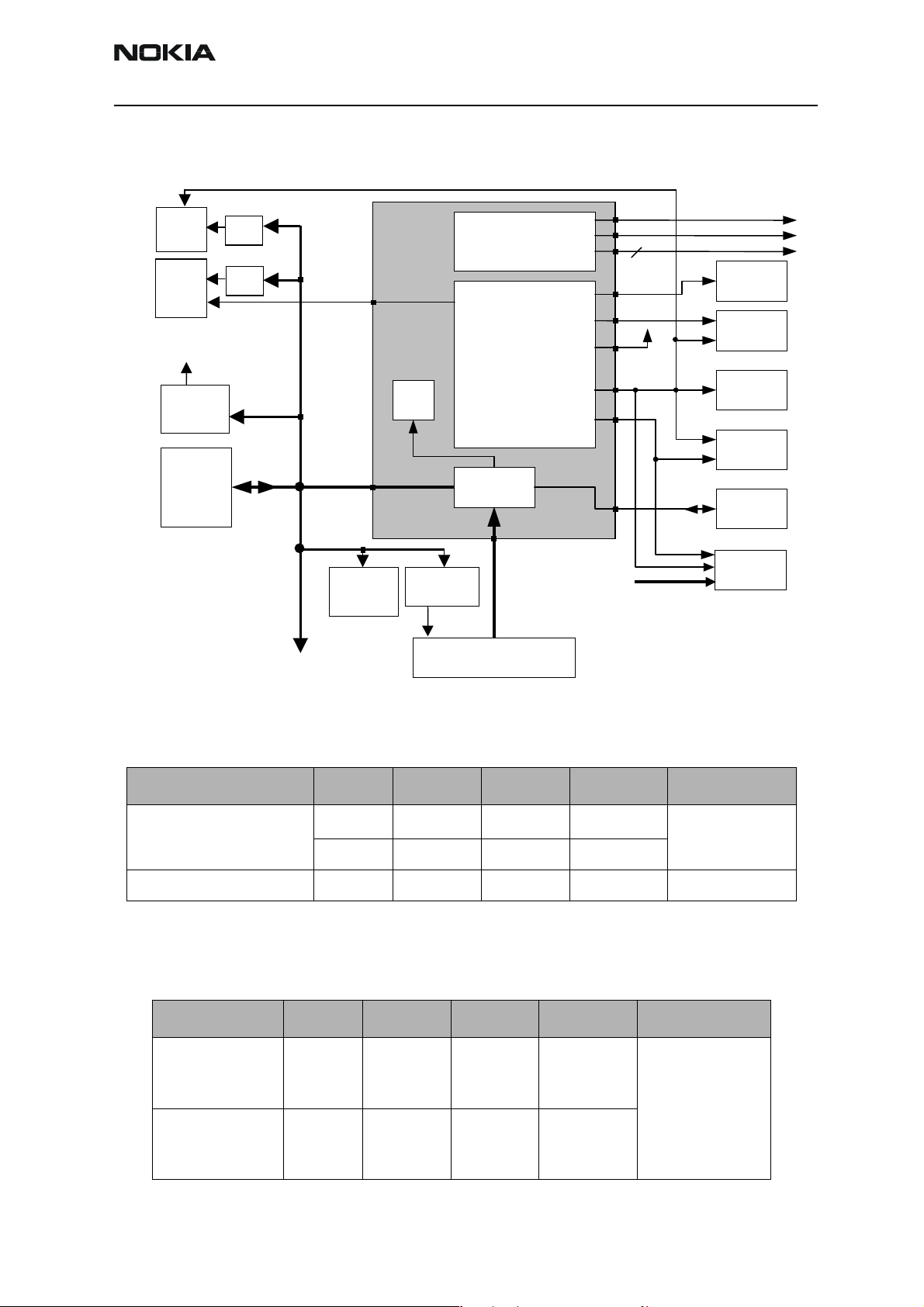
Figure 1: Baseband Block Description
UPP8Mv3
Combo
Memor
FLASH 128Mbit
& utRAM 16MBit
Keyboards
Engine QWERTY
Engine control
Flip T9
C
Flip QW ERTY
LCD
Passive colour STN
Led driver
Keyboard &
display
illumination
SIM
DEMI
RF-BB Interface
UEMK
Edge
1.8 V
Battery
BL-5C
BU
IR
Bluetooth
Vibra
Accessory
Regulator
System connector
DC
ack
IHF
Tomahawk
IHF Amp
LM4890
HWA
Baseband is running from power rails 2.8V analog voltage and 1.8V I/O voltage. UPP core
voltages can be programmed to 1.053V, 1.35V, 1.57V (default) and 1.8V. UEMK includes
a 6-linear LDO (low drop-out) regulator for baseband and 7 regulators for RF. It also
includes 4 current sources for biasing purposes and internal usage. UEMK also includes
SIM interface, which supports both 1.8V and 3V SIM cards.
The baseband architecture supports a power saving function called ”sleep mode”. This
sleep mode shuts off the VCTCXO, which is used as system clock source for both RF and
baseband. During the sleep mode, the system runs from a 32 kHz crystal. The phone is
waken up by a timer running from this 32 kHz clock supply or from external interrupt.
The sleeping time is determined by network parameters. The sleep mode is entered when
both the MCU and the DSP are in standby mode and the normal VCTCXO clock has been
switched off. Bluetooth has its own sleep period that is not aligned with phone sleep.
CSR BC02
Camera
CIF
Page 8 ©Nokia Corporation Issue 1 12/03
NHL-9
CCS Technical Documentation 3 - System Module
A real time clock function is integrated into the UEMK, which utilises the same 32kHz
clock supply as the sleep clock. A backup power supply is provided for the RTC-battery,
which keeps the real time clock running when the main battery is removed. The backup
power supply is a rechargeable surface mounted cell capacitor. The backup time with the
cell capacitor is 15 minutes minimum.
The interface between the baseband and the RF section is mainly handled by a UEMK
ASIC. UEMK provides A/D and D/A conversion of the in-phase and quadrature receive and
transmit signal paths and also A/D and D/A conversions of received and transmitted
audio signals to and from the user interface. The UEMK supplies the analog TXC and AFC
signals to the RF section according to the UPP DSP digital control. Data transmission
between the UEMK and the UPP is implemented using two serial busses, DBUS for DSP
and CBUS for MCU. There are also separate signals for PDM coded audio. Digital speech
processing is handled by the DSP inside UPP ASIC. UEMK is a dual voltage circuit, the
digital parts are running from the baseband supply 1.8V and the analogue parts are running from the analogue supply 2.78V also VBAT is directly used by some specific blocks.
The baseband supports both internal and external microphone inputs and speaker outputs. Input and output signal source selection and gain control is done by the UEMK
according to control messages from the UPP. Keypad tones, DTMF, and other audio tones
are generated and encoded by the UPP and transmitted to the UEMK for decoding. An
external vibra alert control signal is generated by the UEMK with separate PWM output.
NHL-9 has two external serial control interfaces: FBUS and MBUS. FBUS can be accessed
through production test pattern and Pop-PortTM System Connector. FBUS interface and
MBUS can be accessed through the production test pattern.
EMC shielding is implemented using soldered metal cans. Heat generated by the circuitry
is conducted out via ground planes located in the PWB.
The NHL-9 PWB is implemented into an 8-layer selective OSP coated PWB using buried
via technology.
Table 1: NHL-9 GenIO usage
GENIO # Direction Signal Name Connected to
Default
state in
sleep
Note
GenIO0 Out ACIRegEn SysCon “0” ACI regulator enable
GenIO1 Out CamRegEn Camera “0” Camera regulator enable
GenIO2 In COL5 UI “1”, Pull-Up Column 5 input from key-
pad matrix
GenIO3 Out CAMClk Camera “0” Clock for camera module
(13MHz)
GenIO4 Out LCDRst LCD “1” LCD reset
GenIO5 Out TXP RF “0” RF PA control
Issue 1 12/03 ©Nokia Corporation Page 9
NHL-9
3 - System Module CCS Technical Documentation
GenIO6 Out RESET RF “0” RF IC reset
GenIO7 Out TXA RF “0” RF IC control
GenIO8 Out BTRstX Bluetooth “1” BT Reset
GenIO9 Out TXL2 RF “0” RF Mode select
GenIO10 Out BTWakeUp Bluetooth “0” BT wake up
GenIO11 In UPP_BT_CTS Bluetooth “1” BT UART CTS
GenIO12 In BTHostWakeup Bluetooth “0” Engine wake up from BT
GenIO13 Out IHFSD Audio “0” IHF Amplifier Shut down
control
GenIO14 In PCMClk Bluetooth “0” PCM clock
GenIO15 Out PCMIn Bluetooth “0” PCM output
GenIO16 In PCMOut Bluetooth “0” PCM Input
GenIO17 In PCMSync Bluetooth “0” PCM synchronization 8kHz
GenIO18 I/O FlipData Flip “1”, pull-up Data between engine and
flip
GenIO19 In BTUARTRx Bluetooth “1” BT UART input
GenIO20 Out BTUARTTx Bluetooth “1” BT UART output
GenIO21 Out UPP_BT_RTS Bluetooth “1” BT UART RTS
GenIO22 Out FlipClk Flip “0” Clock signal for flip data
GenIO23 Out RAMCSX Memory “0” RAM chip select / flash
write protect
GenIO24 Out IRSD IR “1” Shut down for IrDA
GenIO25 In Shift UI “1”, pull-up Keypad “SHIFT” key
GenIO26 Out CAMSDX Camera “0” Camera shut down control
GenIO27 In CamRxDa Camera “0” Camera data input
GenIO28 Out CAMCSX Camera “0” Camera chip select
GenIO29 Out SIMClkI UEMK “0” Clock for SIM data
GenIO30 Out SIMIOCtrl UEMK “0” Direction control for SIM-
Dai
GenIO31 I/O SIMDaI UEMK “0” SIM data
Page 10 ©Nokia Corporation Issue 1 12/03
NHL-9
CCS Technical Documentation 3 - System Module
Main technical specifications
DC characteristics
Regulators and supply voltage ranges
Table 2: Baseband Regulators
Signal Min Nom Max Note
VANA 2.70V 2.78V 2.86V I
VFLASH1 2.70V 2.78V 2.86V I
VFLASH2 2.70V 2.78V 2.86V I
VSIM 1.745V
2.91V
1.8V
3.0V
1.855V
3.09V
VIO 1.72V 1.8V 1.88V I
VCORE 1.0V
1.283V
1.492V
1.710V
1.053V
1.35V
1.57V
1.8V
1.106V
1.418V
1.649V
1.890V
max
max
I
sleep
max
I
max
I
sleep
max
I
sleep
I
max
I
sleep
Default value 1.57V
Table 3: Accessory Regulator
Signal Min Nom Max Note
= 80mA
= 70mA
= 1.5mA
= 40mA
= 25mA
= 0.5mA
= 150mA
= 0.5mA
= 200mA
= 0.2mA
Vout 2.70V 2.78 2.86V I
= 150mA
max
I
quiescent
< 1.5µA
Enable controlled
through GenIO(0)
Table 4: RF Regulators
Signal Min Nom Max Note
VR1A / VR1B 4.6V 4.75V 4.9V I
VR2 2.70V
3.20V
2.78V
3.3V
2.86V
3.40V
VR3 2.70V 2.78V 2.86V I
VR4 2.70V 2.78V 2.86V I
max
I
max
max
max
I
sleep
= 10mA
= 100mA
= 20mA
= 50mA
= 0.1mA
Issue 1 12/03 ©Nokia Corporation Page 11
NHL-9
3 - System Module CCS Technical Documentation
VR5 2.70V 2.78V 2.86V I
VR6 2.70V 2.78V 2.86V I
VR7 2.70V 2.78V 2.86V I
max
I
sleep
max
I
sleep
max
= 50mA
= 50mA
= 45mA
Table 5: Current Sources
Signal Min Nom Max Note
IPA1 and IPA2 0mA – 5mA Programmable, +/-6%
V
= 0V - 2.7V
IPA1,2
IPA3 and IPA4 95µA 100µA 105µA V
IPA3,4
= 0V - 2.7V
(used internally in the UEMK)
= 0.1mA
= 0.1mA
Table 6: External BT regulator characteristics
Power source Voltage (V)
Max. load
(mA)
Function
Min Typ Max
VBth 2.72 2.80 2.86 70mA From external 2.8V reg-
ulator
VIO 1.72 1.80 1.88 10 mA I/O-voltage to ensure
compatible IO levels.
Table 7: External camera regulator characteristics
Power source Voltage (V)
Max. load
(mA)
Function
Min Typ Max
VCAMDIG 1.72 1.80 1.88 150 mA I/O-voltage to ensure com-
patible IO levels.
Page 12 ©Nokia Corporation Issue 1 12/03
NHL-9
y
CCS Technical Documentation 3 - System Module
Figure 2: Power Distribution Diagram
Baseband
BT
Camera
VLED+
White LED
Driver
Battery
Reg.
2.8V
Reg.
1.8V
VBAT
VBAT
Audio
Amplifier
PA Supply
UEM
RTC
RF Regulators
VFLASH2
Baseband
Regulators
CHACON
Accessory
Regulator
Vout
System Connector
VR1A
VR1B
VR2-7
VSIM
VCORE
VANA
VIO
VFLASH1
6
SIM
UPP
Combo
Memor
LCD
Backup
battery
IRDA
VBAT
Internal signals and connections
Table 8: Internal Microphone
Signal Min Nom Max Condition Note
MICP 200mV
2.0 V 2.1 V 2.25 V DC
MICN 2.0V 2.1V 2.25V DC
Table 9: Internal Speaker
Signal Min Nom Max Condition Note
EARP
0.75V 0.8V
EARN
0.75V 0.8V
2.0 V
0.85V
2.0 V
0.85V
pp
pp
AC 2.2kΩ to MIC1B
pp
AC
DC
AC
DC
Differential output
(V
= 4.0 Vpp)
diff
Issue 1 12/03 ©Nokia Corporation Page 13
NHL-9
3 - System Module CCS Technical Documentation
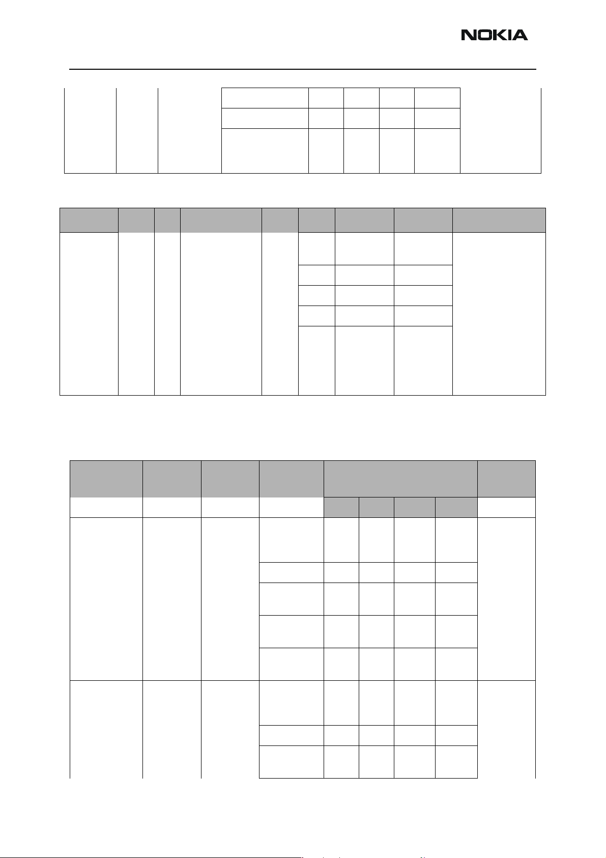
Table 10: AC and DC Characteristics of DCT4 RF-Baseband Voltage Supplies
Signal
name
VBAT Battery PA & UEMK Voltage 3.1 3.7 4.2 V Battery supply
VR1A UEMK HELGO Voltage 4.6 4.75 4.9 V Supply for
VR2 UEMK HELGO Voltage 2.70 2.78 2.86 V Supply for
From To Parameter Min Typ Max Unit Function
GSM900, PL5
Current by PA during TX-on
Current drawn by
PA when ”off”
Current 4 10 mA
Noise density 240 nVrms/
0.8 2 uA
2600 mA
charge pump for
SHF VCO tuning
sqrt(Hz)
I/Q-modulators,
buffers, ALS
Current 100
0.1mAmA
(sleep)
Noise density
f=100Hz
f>300Hz
VR3 UEMK VCTCXO,
HELGO
VR4 UEMK HELGO Voltage 2.70 2.78 2.86 V Supply for Helgo
Voltage 2.70 2.78 2.86 V Supply for
Current 1.5 20 mA
Noise density 240 nVrms/
120 nVrms/
sqrt(Hz)
VCTCXO, PLL digital parts
sqrt(Hz)
RX; PA bias
blocks
Noise density
decades 20dB/
deg from 6Hz to
600 Hz. From
f>600Hz max.
noise density
nVrms/ sqrt(Hz)
Current 50
0.1mAmA
(sleep)
Page 14 ©Nokia Corporation Issue 1 12/03
NHL-9
CCS Technical Documentation 3 - System Module
Noise density
f=6Hz
f=60Hz
f>600Hz
VR5 UEMK HELGO Voltage 2.70 2.78 2.86 V Supply for Helgo
Current 50 mA
Noise density
BW=100Hz...
100kHZ
VR6 UEMK HELGO Voltage 2.70 2.78 2.86 V Supply for Helgo
Current 50
Noise density
BW=100Hz...
100kHz
5500
550
55
240 nVrms/
0.1
240 nVrms/
nVrms/
sqrt(Hz)
sqrt(Hz)
mA
mA
(sleep)
sqrt(Hz)
PLL; dividers, LObuffers, prescaler,
BB and LNAs
VR7 UEMK VCO Voltage 2.70 2.78 2.86 V Supply for SHF
VCO
Current 45 mA
Noise density
100Hz<f<2kHz
2kHz<f<10kHz
10kHz<f<30kHz
30kHz<f<90kHz
90kHz<f<3MHz
VrefRF01 UEMK HELGO Voltage 1.334 1.35 1.366 V Voltage Refer-
70
55
35
30
30
nVrms/
sqrt(Hz)
ence for HELGO
Note: Below
600Hz noise
density is
allowed to
increase 20 dB/
oct
Current 100 uA
Temp Coef -65 +65 uV/C
Noise density
BW=600Hz...
100kHz
VrefRF02 UEMK UEMK Voltage 1.334 1.35 1.366 V Voltage refer-
Note
60 nVrms/
sqrt(Hz)
ence for UEMK
internal use
Issue 1 12/03 ©Nokia Corporation Page 15
NHL-9
3 - System Module CCS Technical Documentation
Current 100 uA
Temp Coefficient -65 +65 uV/C
Noise density
BW=100Hz...
100kHz
Table 11: BB-RF Current Sources
Signal From To Parameter Min Typ Max Unit Function
IPA1 and
IPA2
UEMKPA Current 0 5mA mA Programmable
Voltage 2.7 V Rout _ 540 Ohm
Resolution 4 Bit
Tolerance -6 +6 %
Noise density
100Hz _ f _
800kHz
800kHz _ f _
100MHz
350 nVrms/
sqrt(Hz)
88
110
nVrms/_Hz
(0.3333mA /step)
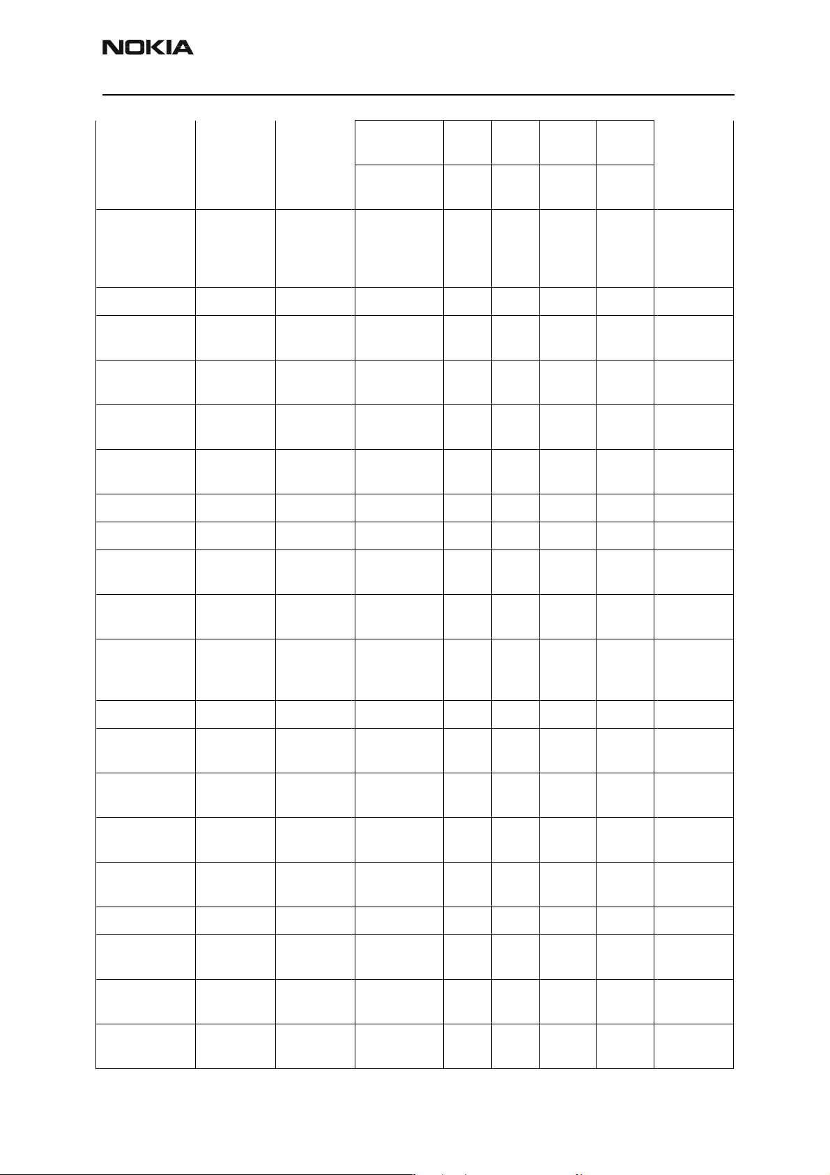
Table 12: AC and DC Characteristics of DCT4 RF-Baseband Digital Signals
Signal name From To Parameter Input Characteristics
Min Typ Max Unit
TXP1
(RFGenOut3)
TXA UPP
UPP
(GenIO5)
(GenIO7)
HELGO ”1” 1.38 1.88 V Power
”0” 0 0.4 V
Load Resistance
Load Capacitance
Timing
Accuracy
HELGO ”1” 1.38 1.88 V Power con-
”0” 0 0.4 V
10 220 kΩ
20 pF
1/4 symbol
Function
amplifier
enable
trol loop
enable
Load Resistance
10 220 kΩ
Page 16 ©Nokia Corporation Issue 1 12/03
NHL-9
CCS Technical Documentation 3 - System Module
Load Capacitance
Timing
Accuracy
MODE UPP
(GenIO9)
RFBusEn1X UPP HELGO ”1” 1.38 1.88 V RFBus ena-
PA ”1” 1.38 1.88 V Power
”0” 0 0.4 V
Load Resistance
Load Capacitance
Timing
Accuracy
”0” 0 0.4 V
Current 50 uA
10 220 kΩ
20 pF
1/4 symbol
amplifier
mode input
20 pF
1/4 symbol
ble
Load resistance
Load capacitance
RFBusDa UPP HELGO ”1” 1.38 1.88 V RFbus
”0” 0 0.4 V
Load resistance
Load capacitance
Data frequency
RFBusClk UPP HELGO ”1” 1.38 1.88 V RFBus
”0” 0 0.4 V
Load resistance
10 220 kΩ
20 pF
data; read/
write
10 220 kΩ
20 pF
10 MHz
clock
10 220 kΩ
Load capacitance
Data frequency
20 pF
10 MHz
Issue 1 12/03 ©Nokia Corporation Page 17
NHL-9
3 - System Module CCS Technical Documentation
RESET UPP
(GENIO06)
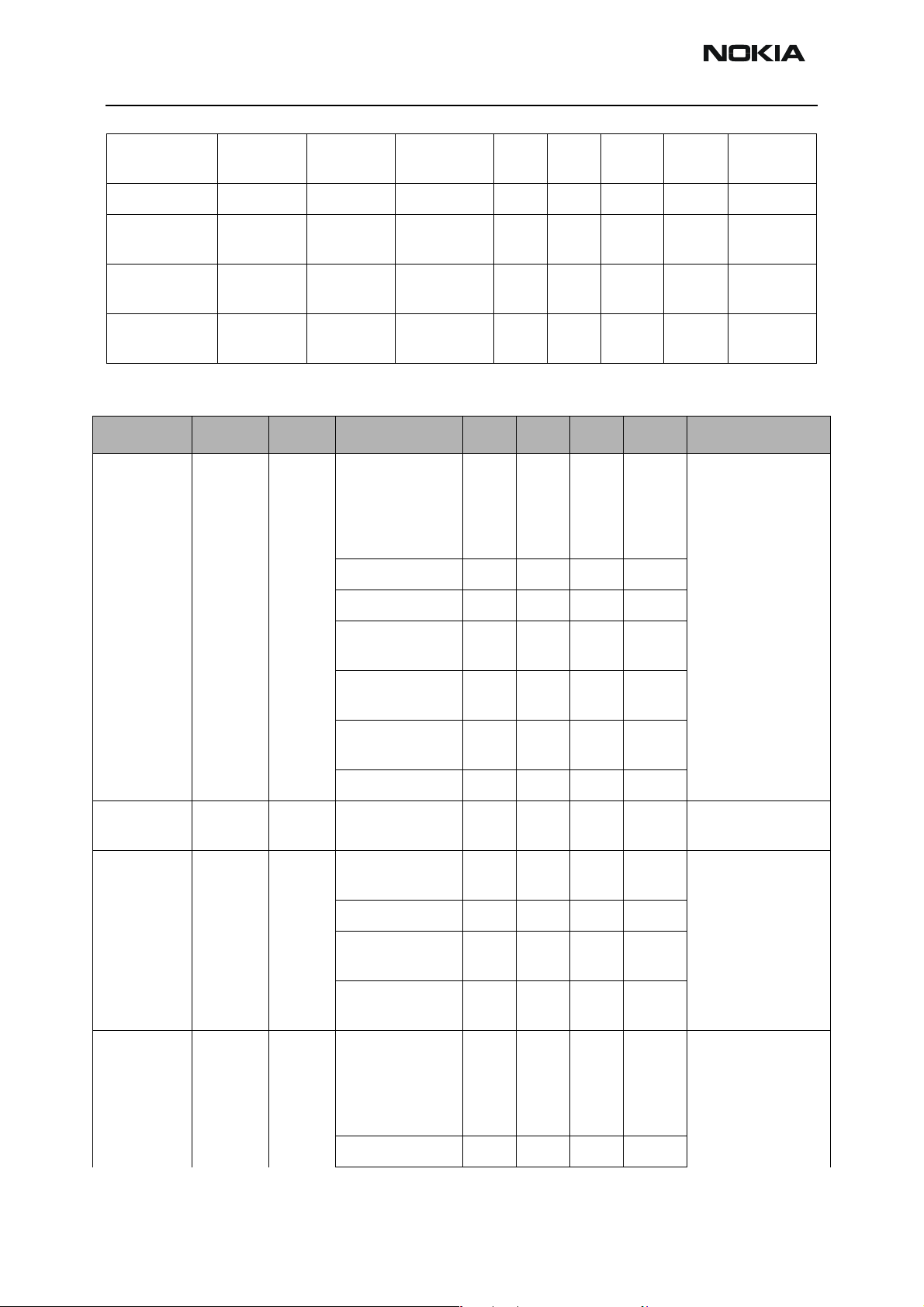
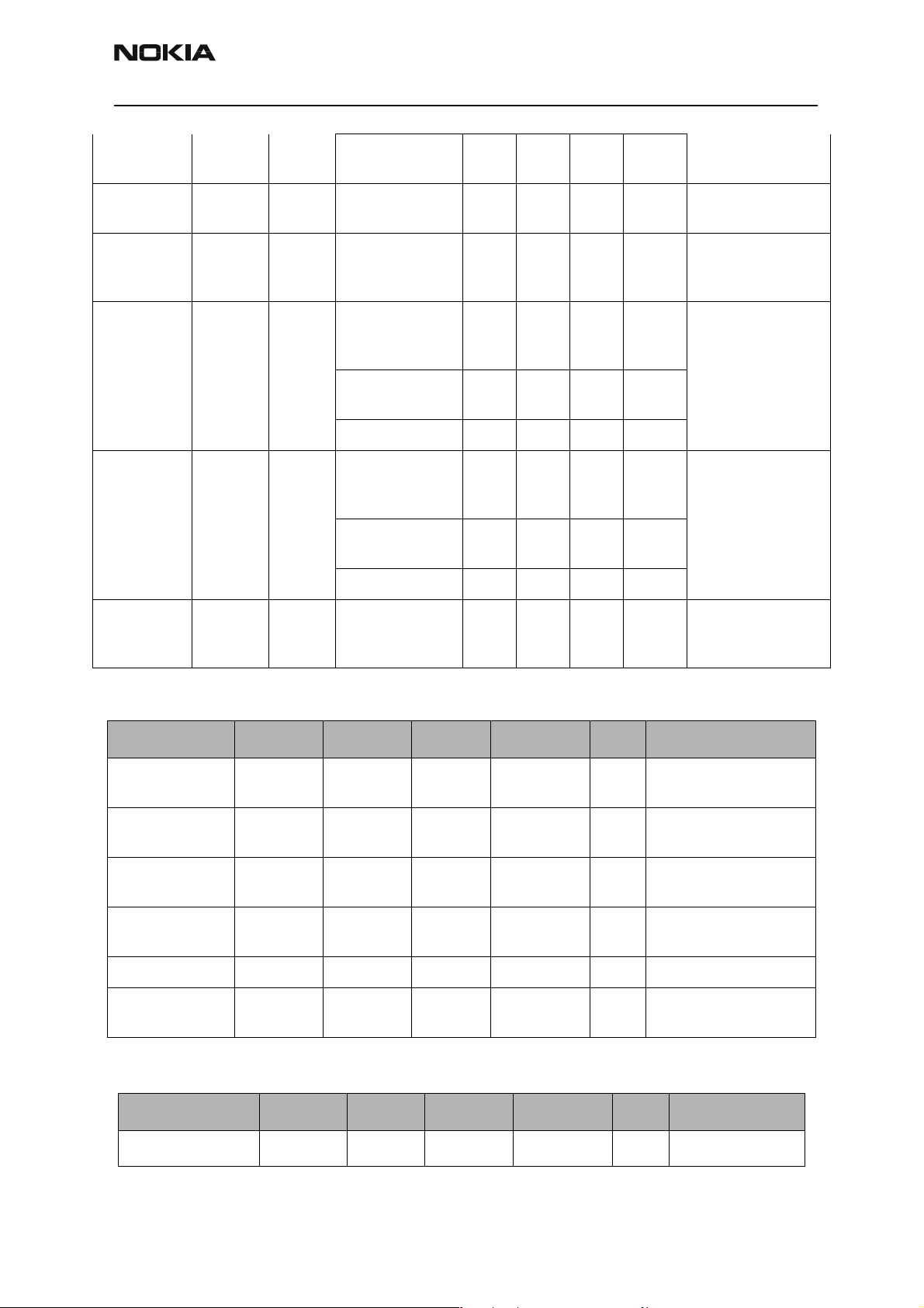
Table 13: AC and DC Characteristics of DCT4 RF-Baseband Analogue Signals
Signal name From To Parameter Min Typ Max Unit Function
VCTCXO VCTCXO UPP Frequency 13 26 MHz High stability clock
HELGO ”1” 1.38 1.85 V Reset to
Helgo
”0” 0 0.4 V
Load capacitance
Load resistance
Timing accuracy
Signal amplitude 0.3 0.8 2.0 Vpp
10 220 kΩ
20 pF
1/4 symbol
signal for the logic
circuits, AC coupled. Distorted sinewave e.g. sawtooth.
Input Impedance 10 kΩ
Input Capacitance
Harmonic Content
Clear signal window (no glitch)
Duty Cycle 40 60 %
VCTCXOGnd VCTCXO UPP DC Level 0 V Ground for refer-
RXI/RXQ HELGO UEMK Voltage swing
(static)
DC level 1.3 1.35 1.4 V
I/Q amplitude
mismatch
I/Q phase mismatch
TXIP / TXIN UEMK HELGO Differential volt-
age swing (static)
200 mVpp
1.35 1.4 1.45 Vpp Received demodu-
-5 5 deg
2.15 2.2 2.25 Vpp Programmable volt-
10 pF
-8 dBc
ence clock
lated IQ signals
0.2 dB
age swing.
Programmable common mode voltage.
Between TXIP-TXIN
DC level 1.17 1.20 1.23 V
Page 18 ©Nokia Corporation Issue 1 12/03
NHL-9
CCS Technical Documentation 3 - System Module
Source Impedance
TXQP / TXQN UEMK HELGO Same spec as for
TXIP / TXIN
AFC UEMK
(AFCOUT)
TxC UEMK
(AUXOUT)
RFTemp HELGO UEMK
VCTCXO Voltage Min
Max
HELGO Voltage Min
Max
Source Impedance
Resolution 10 bits
Voltage at -20oC 1,57 V Temperature sensor
(PATEM
P)
Voltage at
+25oC
Voltage at +60oC 1,79
0.0
2.4
2.4
1,7
200 W
0.1
2.6
0.1 V Transmitter power
200 W
V Automatic fre-
quency control signal for VCTCXO
level and ramping
control
of RF.
DC_sense PA UEMK
(TXPWRDET)
Table 14: Baseband-HWA interface DC characteristics
Signal name Type Min Typical Max Unit Description
CamCSX IN H: 0.7xVIO
LCDCamClk IN H: 0.7xVIO
LCDCamTxDa OUT H: 0.8xVIO
CamRxDa IN H: 0.7xVIO
CamClk IN 0.5Vp-p 1Vp-p VIOp-p V All modes
CamCE IN H: 0.7xVIO
Table 15: Baseband-HWA interface AC Characteristics
Voltage 0.6 V PA final stage quies-
L: 0
L: 0
L: 0
L: 0
L: 0
H: VIO
L: 0.3xVIO
H: VIO
L: 0.3xVIO
H: VIO
L: 0.2xVIO
H: VIO
L: 0.3xVIO
H: VIO
L: 0.3xVIO
V Camera chip-select
(active low)
V Voltage levels
V Data to transmit, camera
interrupt (active low)
V Data to receive
V Logic 0: shutdown.
cent current level
information
Signal name Type Min Typ Max Unit Description
LCDCamCLK IN 0 -
8.8
1
MHz Frequency
Issue 1 12/03 ©Nokia Corporation Page 19
NHL-9
3 - System Module CCS Technical Documentation
45/55 50/50 55/45 % Duty cycle
CamClk IN 8.3 8.4 8.5 MHz External system
clock (mode 1)
9.5 9.6 9.7 MHz External system
clock (mode 2)
9.62 9.72 9.82 MHz External system
clock (mode 3)
12.9 13.0 13.1 MHz External system
clock (mode 4)
16.7 16.8 16.9 MHz External system
clock (mode 5)
45/55 50/50 45/55 % All modes
Table 16: Bluetooth-BB Interface DC Characteristics
I/O-level Voltage Note
Min Typ Max
VIL 0.3 to BT module
VIH 0.7*VIO - -
VOL - - 0.3 From BT module
VOH 0.7*VIO -
Table 17: Bluetooth Clock Specifications
Bluetooth clock Specification
BTClk Single ended input
Frequency 26MHz (VCTCXO)
Min. level 200 mVpp
Max. level 1.8 Vpp (VIO)
Input impedance Input impedance < 4 pF and >10kohm
Phase noise Max. –129 dBc/Hz @ 1 kHz at 26 MHz
Phase Jitter 15ps rms
Settling time Max. 5ms (BTHostWakeUp -> BTClk stabile)
Page 20 ©Nokia Corporation Issue 1 12/03
NHL-9
CCS Technical Documentation 3 - System Module
External signals and connections
Table 18: UI Connector
Pin Signal Min Nom Max Condition Note
16 VDDI 1.72V 1.8V 1.88V Logic voltage supply
Connected to VIO
15 XRES 0.7*VDDI
0
1us t
14 SDA 0.7*VDDI
0
100ns t
100ns t
13 SCLK 0.7*VDDI
0
250ns t
100ns t
100ns t
12 CXS 0.7*VDDI
0
60ns t
VDDI
0.3*VDDI
VDDI
0.3*VDDI
VDDI
0.3*VDDI
6.5MHz
VDDI
0.3*VDDI
Logic ’1’
Logic ’0’
rw
Logic ’1’
Logic ’0’
sds
sdh
Logic ’1’
Logic ’0’
Max frequency
scyc
shw
slw
Logic ’1’
Logic ’0’
css
Reset
Active low
Reset active
Serial data
Data setup time
Data hold time
Serial clock input
Clock cycle
Clock high
Clock low
Chip select
Active low
CXS low before
SCLK rising edge
100ns t
csh
CXS low after SCLK
rising edge
11 GND 0V
10 GND 0V
9 GND 0V
8 GND 0V
7 GND 0V
6 GND 0V
5 VDD VDD 2.70V 2.78V 2.86V Supply Voltage.
Connected to
VFLASH1
4 GND 0V
3 GND 0V
2 VLED- 0V
0.5V
LED off
LED on
Feedback Voltage to
LED Driver
Issue 1 12/03 ©Nokia Corporation Page 21
NHL-9
3 - System Module CCS Technical Documentation
1 VLED+ 0V
9V
LED off
LED on
Supply Voltage for
LEDs
Table 19: FLIP Connector
Pin Signal Min Nom Max Condition Note
1 FLIPCLK 0.7*VIO
0
VIO
0.3*VIO
Logic ’1’
Logic ’0’
Bus clock for flip
module
2 VBAT 3.7V 4.2V Supply for flip µC
3 FLIPDATA 0.7*VIO
0
VIO
0.3*VIO
Logic ’1’
Logic ’0’
I/O data for flip
module
Table 20: DC Connector
Pin Signal Min Nom Max Condition Note
1 VCHAR 11 .1 V
peak
16.9 V
7.9 V
1.0 A
peak
RMS
peak
Standard
charger
Charger positive
input
7.0 V
RMS
8.4 V
RMS
9.2 V
850 mA
RMS
Fast charger
2 CHGND 0 Charger ground
TM
Table 21: Pop-Port
System Connector
Pin Signal Description Spectral Range U/I levels Impedance Notes
1 CHARGE V Charge DC 0-9 V / 0.85 A
2 GND Charge GND 0.85 A 100 mΩ (PWB + conn.)
3 ACI ACI 1 kbit/s Dig 0 / 2.78V 47 Ω Insertion &
removal detection
4 VOUT DC out DC 2.78V / 70mA 100 mΩ (PWB + conn.)
200mW
5 NC DC in DC 4.375-5.25V
6 FBUS RX FBUS 115k FBus 0 / 2.78V 33 Ω
7 FBUS TX FBUS 115k FBus 0 / 2.78V 33 Ω
8 GND Data GND
9 XMIC N Audio in 300 - 8k 1Vpp & 2.78V DC
10 XMIC P Audio in 300 - 8k 1Vpp & 2.78V DC
11 HSEAR N Audio out 20 - 20k 1Vpp 10 Ω
Page 22 ©Nokia Corporation Issue 1 12/03
NHL-9
CCS Technical Documentation 3 - System Module
12 HSEAR P Audio out 20 - 20k 1Vpp 10 Ω
13 NC Not Connected
14 NC Not Connected
Table 22: SIM Connector
Pin Name Parameter Min Typ Max Unit Notes
1 VSIM 1.8V SIM Card 1.62 1.8 1.98 V Supply voltage
3V SIM Card 2.7 3.0 3.3 V
2 SIMRST 1.8V SIM Card 0.8xVSIM
0
3V SIM Card 0.8xVSIM
0
3 SIMCLK Frequency 3.25 MHz SIM clock
Trise/Tfall 50 ns
1.8V Voh
1.8V Vol
3V Voh
3V Vol
4 DATA 1.8V Voh
1.8V Vol
3V Voh
3V Vol
1.8V Vih
1.8V Vil
3V Vil
3V Vil
0.7xVSIM
0
0.7xVSIM
0
0.7xVSIM
0
0.7xVSIM
0
0.7xVSIM
-0.3
0.7xVSIM
-0.3
VSIM
0.2xVSIM
VSIM
0.2xVSIM
VSIM
0.2xVSIM
VSIM
0.2xVSIM
VSIM
0.3
VSIM
0.4
VSIM +0.3
0.2xVSIM
VSIM +0.3
0.2xVSIM
V SIM reset (output)
V
V
V
V SIM data (output)
V
V SIM data (input)
Trise/Tfall max 1us
5 NC Not connected
6 GND GND 0 0 V Ground
Issue 1 12/03 ©Nokia Corporation Page 23

NHL-9
3 - System Module CCS Technical Documentation
Baseband functional description
Modes of operation
NHL-9 baseband engine has six different functional modes:
• No supply
• Back-up
•Acting Dead
•Active
• Sleep
• Charging
No supply
In NO_SUPPLY mode, the phone has no supply voltage. This mode is a result of disconnection of the main and backup batteries or low battery voltage level in both of the batteries.
Phone is exiting from NO_SUPPLY mode when sufficient battery voltage level is detected.
Battery voltage can rise either by connecting a new battery with VBAT > V
connecting charger and charging the battery above V
Back-up
In BACK_UP mode, the backup battery has sufficient charge but the main battery can be
disconnected or empty (VBAT < V
VRTC regulator is disabled in BACK_UP mode. VRTC output is supplied without regulation
from backup battery (VBACK). All the other regulators are disabled in BACK_UP mode.
Acting dead
If the phone is off when the charger is connected, the phone is powered on but enters a
state called ”Acting Dead”. To the user, the phone acts as if it was switched off. A battery
charging alert is given and/or a battery charging indication on the display is shown to
acknowledge the user that the battery is being charged.
and VBACK > VBU
MSTR
MSTR+
COFF
or by
MSTR+
.
).
Active
In the Active mode, the phone is operates normally, scanning for channels, listening to a
base station, transmitting and processing information. There are several sub-states in the
active mode depending on if the phone is in burst reception, burst transmission, if DSP is
working, etc.
In the Active mode, the RF regulators are controlled by SW, which writes the desired settings into UEMK’s registers: VR1A can be enabled or disabled. VR2 can be enabled or dis-
Page 24 ©Nokia Corporation Issue 1 12/03
NHL-9
CCS Technical Documentation 3 - System Module
abled and its output voltage can be programmed to be 2.78V or 3.3V. VR4 -VR7 can be
enabled, disabled, or forced into low quiescent current mode. VR3 is always enabled in
the Active mode.
Table 23: Regulator Controls
Regulator Note
VFLASH1 Enabled
VFLASH2 Controlled by register writing into UEMK register.
Default state is off.
VANA Enabled
Disabled in sleep mode
VIO Enabled
VCORE Enabled
VSIM Controlled by writing into UEMK register.
VR1A Controlled by writing into UEMK register.
Disabled in sleep mode
VR1B Controlled by writing into UEMK register.
Disabled in sleep mode
VR2 Controlled by writing into UEMK register.
Disabled in sleep mode
VR3 Enabled
Disabled in sleep mode
VR4 Enabled
Disabled in sleep mode
VR5 Enabled
Disabled in sleep mode
VR6 Enabled
Disabled in sleep mode
VR7 Enabled
Disabled in sleep mode
IPA1 Controlled by writing into UEMK register.
IPA2 Controlled by writing into UEMK register.
IPA3 Controlled by writing into UEMK register.
Sleep mode
Sleep mode is entered when both MCU and DSP are in stand–by mode. Sleep is controlled by both processors. When SLEEPX low signal is detected, UEMK enters the SLEEP
mode. VCORE, VIO and VFLASH1 regulators are put into low quiescent current mode. All
the RF regulators are disabled in SLEEP. When SLEEPX=1 is detected, UEMK enters the
ACTIVE mode, which activates all functions.
Issue 1 12/03 ©Nokia Corporation Page 25
NHL-9
3 - System Module CCS Technical Documentation
The sleep mode is exited either by the expiration of a sleep clock counter in the UEMK or
by some external interrupt, generated by a charger connection, key press, headset connection, etc.
In the sleep mode, VCTCXO is shut down and a 32 kHz sleep clock oscillator is used as a
reference clock for the baseband.
Charging
Charging can be performed in any operating mode. The battery type/size is indicated by a
resistor inside the battery pack. The resistor value corresponds to a specific battery
capacity. This capacity value is related to the battery technology as different capacity
values are achieved by using different battery technology.
The battery voltage, temperature, size and current are measured by the UEMK controlled
by the charging software running in the UPP.
The charging control circuitry inside the UEMK controls the charging current delivered
from the charger to the battery. The battery voltage rise is limited by turning the UEMK
switch off when the battery voltage reaches 4.2 V. Charging current is monitored by
measuring the voltage drop across a 220 mΩ resistor.
Battery
850 mAh Li-ion battery pack BL-5C is used in NHL-9.
Table 24: BL-5C Characteristics
Description Value
Nominal discharge cut-off voltage 3.1V
Nominal battery voltage 3.7V
Nominal charging voltage 4.2V
Maximum charger output current 850 mA
Minimum charger output current 200 mA
Cell pack impedance -20 ... 0 °C 200mΩ max
Cell pack impedance 0 ...+20 °C 150mΩ max
Cell pack impedance +20 ...+45 °C 120mΩ max
Cell pack impedance +40 ...+60 °C 150mΩ max
Cell pack impedance +60 ...+80 °C 160mΩ max
Discharge Temperature -20 °C… +70 °C
Charging Temperature -30 °C… +60 °C
Page 26 ©Nokia Corporation Issue 1 12/03
NHL-9
CCS Technical Documentation 3 - System Module
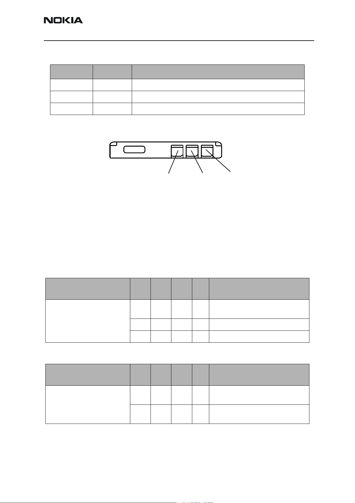
Table 25: Pin Numbering of Battery Pack
Signal name Pin number Function
VBAT 1 Positive battery terminal
BSI 2 Battery capacity measurement (fixed resistor inside the battery pack)
GND 3 Negative/common battery terminal
Figure 3: BL-5C Battery Pack Contacts
3(GND)
1 (+)2(BSI)
The BSI fixed resistor value indicates type and default capacity of a battery. NTC-resistor
measures the battery temperature.
Temperature and capacity information is needed for the charge control. BSI is connected
to a pin in the battery connector. BTEMP is connected to NTC resistor. NTC is located on
the engine PWB. Phone has 100 kΩ pull-up resistors for these lines so that they can be
read by A/D inputs in the phone.
Table 26: BSI Resistor Values
Parameter Min Typ Max
Battery size indicator resistor
BSI
6.7 6.8 6.9 kΩ Test mode resistor value
3.2 3.3 3.4 kΩ Local mode resistor value
75 kΩ Battery size indicator (BL-5C)
Uni
t
Notes
Tolerance ±1%
Table 27: BTEMP NTC Resistor Properties
Parameter Min Typ Max
NTC resistor BTEMP 47 kΩ Battery temperature indicator (NTC
4050 K Beta value (B).
Uni
Notes
t
pulldown) ±5% @ 25°C
Tolerance ±3%, +25°C / +85°C
Issue 1 12/03 ©Nokia Corporation Page 27
NHL-9
3 - System Module CCS Technical Documentation
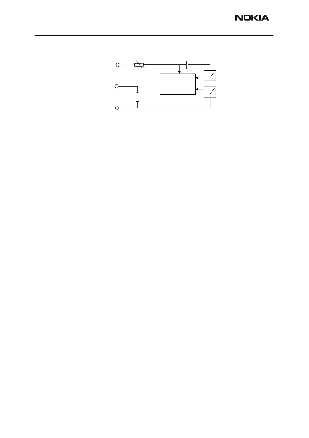
Figure 4: Interconnection diagram
Charging
Supported chargers are ACP-7, ACP-8, ACP-9, ACP-12, LCH-8, LCH-9 and LCH-12.
Charging is controlled by the UEMK ASIC. External components are needed for current
sensing, EMC, reverse polarity and transient protection of the input to the baseband
module. The charger is connected to the system connector interface. The NHL-9 baseband is designed to support DCT3 chargers. Both 2- and 3-wire type chargers are supported.
The operation of the charging circuit has been specified in such a way as to limit the
power dissipation across the charge switch and to ensure safe operation in all modes.
VBATT
GND
BSI
Li-Ion
Overcharge /
Overdischarge
protection
Page 28 ©Nokia Corporation Issue 1 12/03
 Loading...