

Page 1

Nokia Customer Care
RH-47 Series Cellular Phones
6 - Baseband Description and
Troubleshooting
Issue 1 05/04 Copyright © 2004 Nokia Corporation Page 1
Company Confidential
Page 2

RH-47 Company Confidential
7 - Baseband Description & Troubleshooting Nokia Customer Care
[This page intentionally blank]
Page 2 Copyright© 2004 Nokia Corporation Issue 1 05/04
Company Confidential
Page 3

Company Confidential RH-47
Nokia Customer Care 6 - Baseband Description and Troubleshooting
Table of Contents
Page No
List of abbreviations ............................................................................................................................... 4
1CK System Module Block Diagram................................................................................................... 6
Baseband Technical Summary ............................................................................................................. 7
Functional Description ........................................................................................................................... 8
BB description .......................................................................................................................................8
Memory configuration ..................................................................................................................... 8
Energy management......................................................................................................................... 8
Modes of operation ..............................................................................................................................8
Voltage limits...................................................................................................................................... 9
Clocking scheme ...................................................................................................................................9
UPP_WD2 voltage/clock frequency adjusting ........................................................................ 10
Power distribution, control and reset ...........................................................................................10
Power-up sequence (reset mode)............................................................................................... 10
Powering off..................................................................................................................................... 11
Uncontrolled powering off......................................................................................................
Watchdogs........................................................................................................................................ 11
Charging............................................................................................................................................ 11
Chargers............................................................................................................................................. 12
Battery ............................................................................................................................................... 12
Back-up battery and real time clock ............................................................................................12
Baseband measurement A/D converter ........................................................................................12
ZOCUS ....................................................................................................................................................12
RH-47 BB Features & HW Interfaces.............................................................................................. 13
RH-47 BB user interface ..................................................................................................................13
UI module interface ....................................................................................................................... 13
Bluetooth ..............................................................................................................................................13
SIM interface .......................................................................................................................................13
MMC interface ....................................................................................................................................14
RH-47 audio concept ........................................................................................................................14
Earpiece .......................................................................................................................
Microphone ...................................................................................................................................... 15
Audio amplifier and MALT speaker............................................................................................ 16
External audio interface ............................................................................................................... 16
Flashing .................................................................................................................................................17
Testing interfaces ...............................................................................................................................17
Electrical Specifications for power supply interface in product testing......................... 17
Extreme voltages ...............................................................................................................................18
Temperature conditions ....................................................................................................................18
Humidity and water resistance ......................................................................................................18
Introduction to RH-47 Baseband Troubleshooting..................................................................... 19
General guidelines for RH-47 troubleshooting ..........................................................................19
Tools needed for troubleshooting .............................................................................................. 19
General guidelines.......................................................................................................................... 19
Nominal current consumption ........................................................................................................20
Troubleshooting Paths......................................................................................................................... 21
Dead or jammed device .........................................................................................................
Partially damaged device .................................................................................................................22
...................... 15
..... 11
...........21
Issue 1 05/04 Copyright © 2004 Nokia Corporation Page 3
Company Confidential
Page 4

RH-47 Company Confidential
7 - Baseband Description & Troubleshooting Nokia Customer Care
Most common symptoms reported by customer .......................................................................22
Most common symptoms for audio problems........................................................................ 22
Most common symptoms for Bluetooth problems................................................................ 22
Symptoms related to energy management ............................................................................. 22
Problems related to UI module:.................................................................................................. 22
Most common RF related symptoms: ....................................................................................... 23
ASIC is changed ..................................................................................................................................23
Test points ............................................................................................................................................24
“CONTACT SERVICE” on display ......................................................................................................25
1CK Baseband HW Subarea Troubleshooting............................................................................... 26
Flashing troubleshooting ..................................................................................................................26
Energy management troubleshooting ..........................................................................................28
Device does not stay on................................................................................................................ 28
General power checking ............................................................................................................... 29
Power key troubleshooting .......................................................................................................... 31
Clocks troubleshooting.................................................................................................................. 31
Charging checking..............................................................................................................
Energy management calibration ................................................................................................ 37
ADC-reading..................................................................................................................................... 38
Backup battery ................................................................................................................................ 38
SIM card ............................................................................................................................................ 40
Audio troubleshooting ......................................................................................................................43
Memory troubleshooting ..................................................................................................................50
Serial interface troubleshooting ....................................................................................................50
CBUS................................................................................................................................................... 50
FBUS ................................................................................................................................................... 51
MBUS.................................................................................................................................................. 51
Bluetooth troubleshooting ...............................................................................................................52
MMC troubleshooting .......................................................................................................................53
Vibra .......................................................................................................................................................54
ZOCUS ....................................................................................................................................................55
UI Module Troubleshooting ......................................................................................................
Keymat backlight ................................................................................................................................56
Keyboard problem ..............................................................................................................................58
Display blank ........................................................................................................................................59
Backlight does not turn on .............................................................................................................60
Appendix A ............................................................................................................................................. 62
Test points - Bottom ..........................................................................................................................62
Test points - Top .................................................................................................................................62
............ 34
......... 56
Page 4 Copyright © 2004 Nokia Corporation Issue 1 05/04
Company Confidential
Page 5

Company Confidential RH-47
Nokia Customer Care 6 - Baseband Description and Troubleshooting
List of abbreviations
ASIC Application Specific Integrated Circuit
BB Baseband
BT Bluetooth
BSI Battery Size Indicator
CBus Control Bus connecting UPP_WD2 with UEM
CPU Central Processing Unit
DBUS Data Bus
DSP Digital Signal Processor
ESD Electro Static Discharge
GPRS General Packet Radio Service
GSM Group Special Mobile/Global system mobile
HF Hands free
HFCM Handsfree Common
HS Handset
I/O Input/Output
IHF Integrated hands free
LCD Liquid Crystal Display
LO Local Oscillator
MCU Micro Controller Unit
MIC, mic Microphone
PA Power Amplifier
PCS GSM1900
PDA Pocket Data Application
PLL Phase Locked Loop
Issue 1 05/04 Copyright © 2004 Nokia Corporation Page 5
Company Confidential
Page 6

RH-47 Company Confidential
7 - Baseband Description & Troubleshooting Nokia Customer Care
PWB Printed Wired Board
RFBUS Control Bus For RF RXReceiver
SDRAM Synchronous Dynamic Random Access Memory
SIM Subscriber Identity Module
TX Transmitter
UEM Universal Energy Management
UI User Interface
VCO Voltage controlled oscillator
VHF Very High Frequency
VCXO Voltage Controlled Crystal Oscillator
VGA Video Graphics Array
Page 6 Copyright © 2004 Nokia Corporation Issue 1 05/04
Company Confidential
Page 7
Company Confidential RH-47
Nokia Customer Care 6 - Baseband Description and Troubleshooting
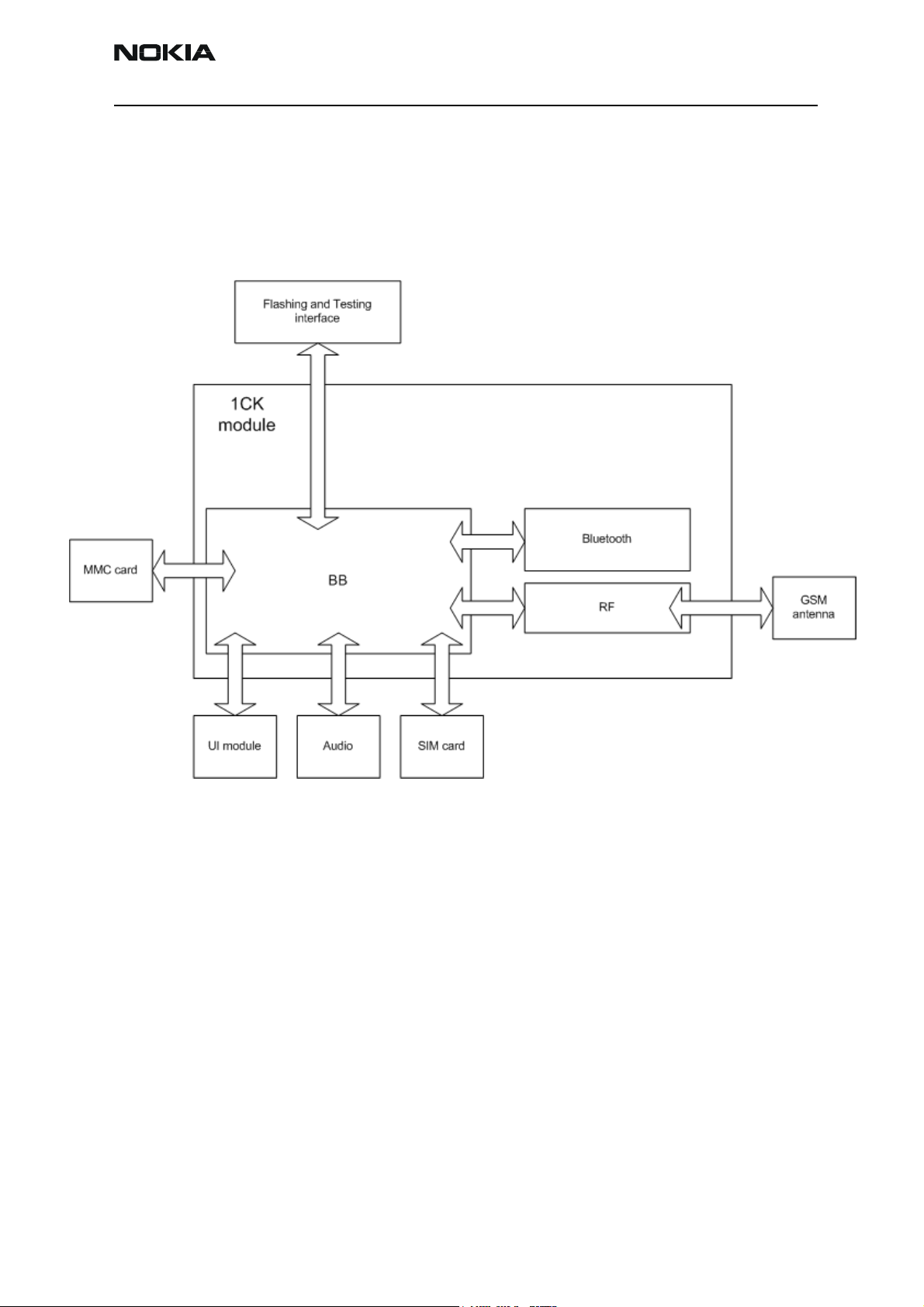
1CK System Module Block Diagram
The 1CK system module is the engine board of the RH-47 phone. It includes the baseband and RF functions of the phone and the Bluetooth module, fig. 1 below. External
interfaces are drawn as arrows crossing the 1CK border.
Figure 1: 1CK module block diagram
The accessory interface is provided by Bluetooth. Only the headset & charger are galvanic interfaces.
Issue 1 05/04 Copyright © 2004 Nokia Corporation Page 7
Company Confidential
Page 8

RH-47 Company Confidential
7 - Baseband Description & Troubleshooting Nokia Customer Care
Baseband Technical Summary
The heart of the BB is UPP_WD2, which includes the MCU, DSP and digital control logic.
Power is supplied by the UEMK ASIC and a number of discrete regulators. Memory comprises 1x 64Mbit, 1x 128Mbit flash memory devices and 128Mbit SDRAM.
There are two audio transducers (earpiece 8 mm and a MALT speaker 16 mm) and external galvanic headset (DCT4) interface. MALT speaker is also used for handling the ringing
tones. The MALT speaker is driven by a discrete audio amplifier.
For data connectivity, there is Bluetooth and an MMC card.
The display is a GD82C type colour display with 66000 Colours and 176x208 pixels with
backlighting.
Page 8 Copyright © 2004 Nokia Corporation Issue 1 05/04
Company Confidential
Page 9

Company Confidential RH-47
Nokia Customer Care 6 - Baseband Description and Troubleshooting
Functional Description
BB description
The BB core is based on UPP_WD2 CPU, which is a PDA version of the DCT4 UPP ASIC.
UPP_WD2 takes care of all the signal processing and operation controlling tasks of the
phone as well as all PDA tasks.
For power management, there is one main ASIC for controlling charging and supplying
power UEM plus some discrete power supplies. The main reset for the system is generated by the UEM.
The interface to the RF and audio sections is also handled by the UEM. This ASIC provides
A/D and D/A conversion of the in-phase and quadrature receive and transmit signal
paths and also A/D and D/A conversions of received and transmitted audio signals. Data
transmission between the UEM and RF and the UPP_WD2 is implemented using different
serial connections (CBUS, DBUS, FBUS, MBUS and RFBUS). Digital speech processing is
handled by the UPP_WD2 ASIC.
A real time clock function is integrated into the UEM, which utilizes the same 32kHzclock source as the sleep clock. A rechargeable battery provides backup power to run the
RTC when the main battery is removed. Backup time is about 3 hours.
Memory configuration
RH-47 uses two kinds of memories: flash and SDRAM. These memories have their own
dedicated bus interfaces to UPP_WD2.
Synchronous DRAM is used as working memory. Interface is a 16-bit wide data and 14bit address. Memory clocking speed is 104 MHz. The SDRAM size is 128Mbits (8Mx16).
SDRAM I/O is 1.8 V and core 2.78 V, both are supplied by UEM regulator VIO. All memory
contents are lost, if the supply voltage is switched off.
Multiplexed flash memory interface is used to store the MCU program code and user
data. The memory interface is a burst type FLASH with multiplexed address/data bus,
running at 40MHz. Both Flash I/O and core voltage are 1.8 V supplied by UEM’s VIO.
Energy management
The master of EM control is UEM and with SW this has the main control of the system
voltages and operating modes.
Modes of operation
RH-47 employs several hardware & SW controlled operation modes. The main modes are
described below.
• NO_SUPPLY mode means that the main battery is not present or its voltage is too
low (below UEM master reset threshold) and back-up battery voltage is too low.
• In BACK_UP mode, the main battery is not present or its voltage is too low but
Issue 1 05/04 Copyright © 2004 Nokia Corporation Page 9
Company Confidential
Page 10
RH-47 Company Confidential
7 - Baseband Description & Troubleshooting Nokia Customer Care
back-up battery has sufficient charge in it.
• In PWR_OFF mode, the main battery is present and its voltage is over UEM master reset threshold. All regulators are disabled.
• RESET mode is a synonym for start-up sequence and contains in fact several
modes. In this mode, regulators and oscillators are enabled and after they have
stabilized system reset is released and PWR_ON mode entered.
• In PWR_ON mode, SW is running and controlling the system.
• SLEEP mode is entered from PWR_ON mode when the system’s activity is low
(SLEEPX controlled by SW).
• FLASHING mode is for production SW download.
Voltage limits
In the following table, the voltage limits of the system are listed. These are also controlling system states.:
Parameter Description Value
V
MSTR+
V
MSTR-
V
COFF+
V
COFF-
V_BU
V_BU
SW
COFF
COFF+
COFF-
Master reset threshold (rising) 2.1 V (typ.)
Master reset threshold (falling) 1.9 V (typ.)
Hardware cutoff (rising) 3.1 V (typ.)
Hardware cutoff (falling) 2.8 V (typ.)
Back-up battery cutoff (rising) 2.1 V (typ.)
Back-up battery cutoff (falling) 2.0 V (typ.)
SW cutoff limit (> regulator drop-out limit) MIN! 3.4 V SW changeable
The master reset threshold controls the internal reset of the UEM. If battery voltage is
above V
from the main battery. Above V
, UEM’s charging control logic is alive. In addition, RTC is active and supplied
MSTR
UEM allows the system to be powered on although
MSTR
this may not succeed due to voltage drops during start-up. SW can also consider battery
voltage too low for operation and power down the system.
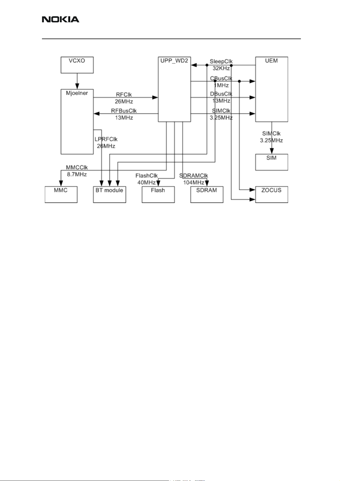
Clocking scheme
A 26 MHz VCXO is used as system clock generator in GSM. During the system start-up,
UEM RC-oscillators generate timing for state machines. All clock signals of the engine
are illustrated in following figure.
Bluetooth uses a 26 MHz clock.
Page 10 Copyright © 2004 Nokia Corporation Issue 1 05/04
Company Confidential
Page 11
Company Confidential RH-47
Nokia Customer Care 6 - Baseband Description and Troubleshooting
Figure 2: RH-47 Clocking.
In SLEEP mode, the VCXO is off. UEM generates low frequency clock signal (32.768 kHz)
that is fed to UPP_WD2, Bluetooth and ZOCUS.
UPP_WD2 voltage/clock frequency adjusting
No external clock is available for UPP_WD2 before VCXO starts. As reset is released, the
VCXO is running and MCU uses the 26 MHz clock while DSP is in reset. There are three
identical DPLL's, for MCU, for DSP and for accessory interfaces which can be controlled
independently. The clock for MCU can be up to 104 MHz and 117 MHz is the maximum
clock frequency for the DSP. These clock signals are used either directly (SDRAM IF) or
divided down for the interfaces (for example, flash IF).
Power distribution, control and reset
All power (except backup battery power) is drawn from the BL-6C Li-Ion battery located
in the B-cover. Current flows through ZOCUS current sense the resistor which is used for
current measurement by ZOCUS and thus for remaining operating time estimation.
1CK board contains one power ASIC, UEM and discrete regulators needed for generating
the different operating voltages. The discrete regulators consist of a step-down DC-DC
converter to power UPPWD2 voltage core and a step-up DC-DC converter for display
module backlighting. The keyboard backlighting is powered with a discrete driver.
Power-up sequence (reset mode)
RESET mode can be entered in four ways: by inserting the battery or charger, by RTC
alarm or by pressing the power key. The VCXO is powered by the UEM. After a 220 ms
delay, regulators are configured and UEM enters the PWR_ON mode and system reset
PURX is released.
During system start-up, in the RESET state, the regulators are enabled, and each regula-
Issue 1 05/04 Copyright © 2004 Nokia Corporation Page 11
Company Confidential
Page 12

RH-47 Company Confidential
7 - Baseband Description & Troubleshooting Nokia Customer Care
tor charges the capacitor(s) at the output with the maximum current (short circuit current) it can deliver. This results in battery voltage dropping during start-up. When a
battery with voltage level just above the hardware cutoff limit is inserted, the system
may not start due to excessive voltage dipping. Dropping below 2.8 V for longer than 5
ms forces the system to PWR_OFF state.
Powering off
Controlled powering off is done when the user requests it by pressing the power-key or
when the battery voltage falls too low. Uncontrolled powering off happens when the
battery is suddenly removed or if over-temperature condition is detected in regulator
block while in RESET mode. In this mode, all UEM’s regulators are disabled immediately
and discrete regulators are disabled as Vbat supply disappears.
Controlled powering off
For RH-47, powering off is initiated by pressing the power key. After that power off
sequence is activated in the UEM and SW. Basically, power key causes a UEM Interrupt to
UPP_WD2 and SW sets watchdog time value to zero and as this happens, PURX is forced
low and all regulators are disabled. If the battery voltage falls below the very last SWcutoff level, SW will power off the system by letting the UEM’s watchdog elapse. If thermal shutdown limit in UEM regulator block is exceeded, the system is powered off. System reset PURX is forced low.
Uncontrolled powering off
This happens when the battery is suddenly removed. UEM’s state machine notices battery
removal after battery voltage has been below V
mode. PURX is set low and all UEM’s regulators are disabled.
Watchdogs
There are three watchdogs in the UEM. The first one is for controlling system power-on
and power-down sequences. The initial time for this watchdog after reset is 32s and the
watchdog can not be disabled. The time can be set using a register. This watchdog is used
for powering the system off in a controlled manner. The other one is for security block
and is used during IMEI code setting. The third one is a power key watchdog. It is used to
power off the system in case SW is stuck and the user presses the power key.
There is also a”soft watchdog” in UPP_WD2. It is used to reset the chip in case software
gets stuck for any reason. The Bluetooth module also contains a watchdog.
Charging
Charging control and charge switch is in the UEM. There are two different charging
modes: charging empty battery (start-up charge mode), and SW controlled charging.
for 5 us and enters the PWR_OFF
COFF-
UEM digital part takes care of charger detection (generates interrupt to UPP_WD2),
pulse width modulated charging control (for internal charge switch) and over voltage
and current detection. SW using registers controls all these.
Page 12 Copyright © 2004 Nokia Corporation Issue 1 05/04
Company Confidential
Page 13

Company Confidential RH-47
Nokia Customer Care 6 - Baseband Description and Troubleshooting
Chargers
RH-47 BB supports a standard charger (two wires), chargers ACP-8 and ACP-12, cigarette charger LCH-8 and LCH-12 are supported.
Battery
RH-47 uses a detachable, semi-fixed lithium-Ion BL-6C battery. Nominal voltage is 3.7 V
(max charging voltage 4.2 V).
The interface consists of three pins: VBAT, GND and BSI. Pull-down resistor inside the
batteries (BSI signal) recognizes the battery types. Voltage level at BSI line is measured
using UEM's AD-converter.
Back-up battery and real time clock
Real time clock (RTC), crystal oscillator and back-up battery circuitry reside in the UEM.
A register in the UEM controls back-up battery charging. Charging is possible only in the
POWER_ON state.
Baseband measurement A/D converter
The UEM contains 11 channels A/D converter, which is used for different baseband measurement purposes. The resolution of A/D converter is 10 bits. Converter uses the CBUS
interface clock signal for the conversion. An interrupt is given to the MCU at the end of
the measurements. The converter is used for following purposes.
• Battery voltage measurement A/D channel (Internal)
• Charger voltage measurement A/D channel (Internal)
• Charger current measurement A/D channel (Internal)
• Battery temperature measurement A/D channel (External)
• Battery size measurement A/D channel (External)
• LED temperature measurement A/D channel (External)
There is also auxiliary AD converter in the UEM, which is used to monitor RF functions.
ZOCUS
The ZOCUS device is a current sensor used for the battery bar display and for determining
whether the phone is in a high current consuming mode. The ZOCUS device measures the
voltage drop across a sense resistor in the battery voltage line. This sense resistor is
formed from a PWB track and is on an internal layer of the PWB. The nominal value of
the sense resistor is 3.3 mohm. ZOCUS reports the current measurement to UPP_WD2 via
the Cbus interface.
Issue 1 05/04 Copyright © 2004 Nokia Corporation Page 13
Company Confidential
Page 14
RH-47 Company Confidential
7 - Baseband Description & Troubleshooting Nokia Customer Care
RH-47 BB Features & HW Interfaces
RH-47 BB user interface
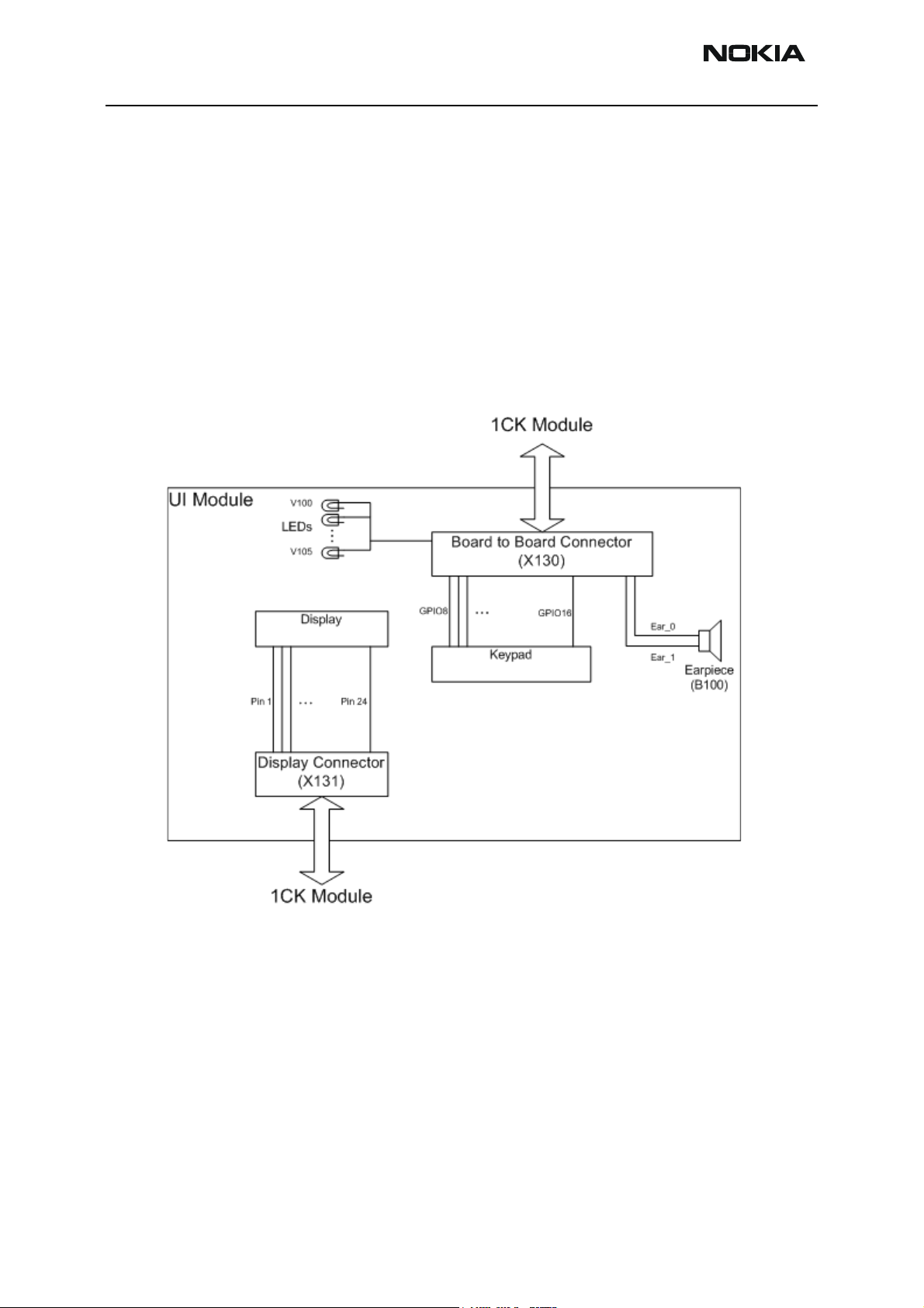
UI module interface
The UI module consists of the LCD and keymat. Colour display resolution is 176 x 208
and backlighting is via 6 orange LED’s with a lightguide. The display is connected to the
1CK module via an24-pin plug and socket. The keymat is connected to 1CK by 24-pin
board-to-board connector. Interface also includes power rails for keypad backlight. The
keymat interface uses GPIO pins of UPP_WD2.
Figure 3: UI module block diagram
Bluetooth
Bluetooth provides a fully digital link for communication between a master unit and one
or more slave units. The system provides a radio link that offers a high degree of flexibility to support various applications and product scenarios. Data and control interface for
a low power RF module is provided. Data rate is regulated between the master and the
slave.
SIM interface
The SIM interface is located in two chips (UPP_WD2 and UEM). In UEM, there is only
support for one SIM card. The interfaces support both 1.8 V and 3 V SIM cards. Adjustable SIM regulator (1.8V/3.0V) is located in the UEM.
Page 14 Copyright © 2004 Nokia Corporation Issue 1 05/04
Company Confidential
Page 15

Company Confidential RH-47
Nokia Customer Care 6 - Baseband Description and Troubleshooting
The data communication between the card and the phone is asynchronous half duplex.
The clock supplied to the card is 3.25 MHz. The data baud rate is SIM card clock frequency divided by 372 (by default), 64, 32 or 16.
MMC interface
The MMC interface consists of a block in UPP_WD2 plus a level shifting device and an
EMC protection ASIP. The MMC interface comprises 3 lines -clock, data and command.
The interface runs at 8.66 MHz. The level shifting device also incorporates a 2.85V regulator to power the MMC card.
Use only multimedia cards (MMC) with this device. Other memory cards, such as Secure
Digital (SD) cards, do not fit in the MMC card slot and are not compatible with this
device.
Using an incompatible memory card may damage the memory card as well as device, and
data stored on the incompatible card may be corrupted.
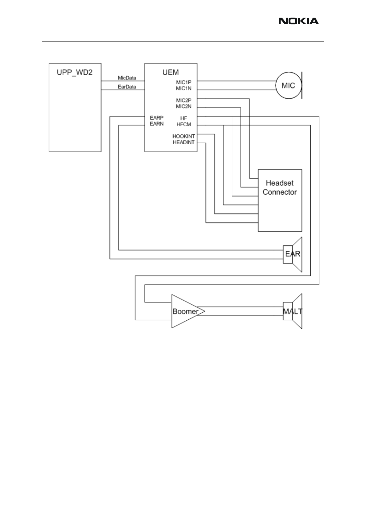
RH-47 audio concept
RH-47 audio includes earpiece, microphone, and headset connector and MALT speaker.
Audio is based on ASIC's UPP_WD2, UEM and a discrete amplifier for the handsfree
speaker.
Issue 1 05/04 Copyright © 2004 Nokia Corporation Page 15
Company Confidential
Page 16
RH-47 Company Confidential
7 - Baseband Description & Troubleshooting Nokia Customer Care
Figure 4: RH-47 Audio Blocks
Between UPP_WD2 and UEM the audio signals are transferred in digital format using
signals MICDATA and EARDATA. The headset output of UEM is also fed to boomer, that is,
the MALT speaker and the headset share the same output lines from UEM. Ringing tones
and warning/info tones are produced with the MALT speaker also.
Earpiece
The earpiece used in RH-47 is an 8-mm Pico earpiece. It has 32Ω continuous impedance
and continuous power 8 mWatt. It is driven by differential signals from the UEM (EARP &
EARN). It makes contact with the PWB via spring contacts.
Microphone
The microphone capsule for RH-47
is an EMC microphone. It has sensitivity of 42db nom-
inal. Contacts are done by springs.
Two inputs are used from the UEM: one for the normal internal microphone and a second
for the headset. The third microphone input is not used, so it is connected to ground via
Page 16 Copyright © 2004 Nokia Corporation Issue 1 05/04
Company Confidential
Page 17
Company Confidential RH-47
Nokia Customer Care 6 - Baseband Description and Troubleshooting
capacitors. Microphone bias block in the UEM generates bias voltages for handportable
and handsfree/headset microphones. For both microphone bias outputs (MICB1 &
MICB2), the minimum output voltage is 2.0 Volts and maximum output current is 600
µA. Microphone bias block also includes a low pass filter for the reference voltage used
as an input for the MICB1&2 amplifiers.
Audio amplifier and MALT speaker
The speaker used in RH-47 is a 16mm 8Ω speaker. It can handle 0.2 Watts nominal
power and peak power 0.3 Watts. The component is housed in the B-cover and connects
to the PWB via spring contacts.
HF and HFCM lines of UEM are use to drive the amplifier.
Power amplifier is a differential opamp. The differential output drives the MALT speaker.
The amplifier load impedance is 8 ohm.
The outputs go into a high impedance state when powered down. The amplifier can be
enabled and shut down using a GENIO line from UPP_WD2.
SW controls IHF and earpiece volume via UEM. Gain setting can be done in 2 dB steps,
from –40 to +6 dB. Output sound pressure level of the MALT speaker is controlled by SW
(CBus is used for controlling).
The schematic around the amplifier is presented in RH-47 schematics. The schematic
shows all the filtering needed and also protection components against ESD and EMC.
The supply voltage for the amplifier is taken directly from the battery voltage.
External audio interface
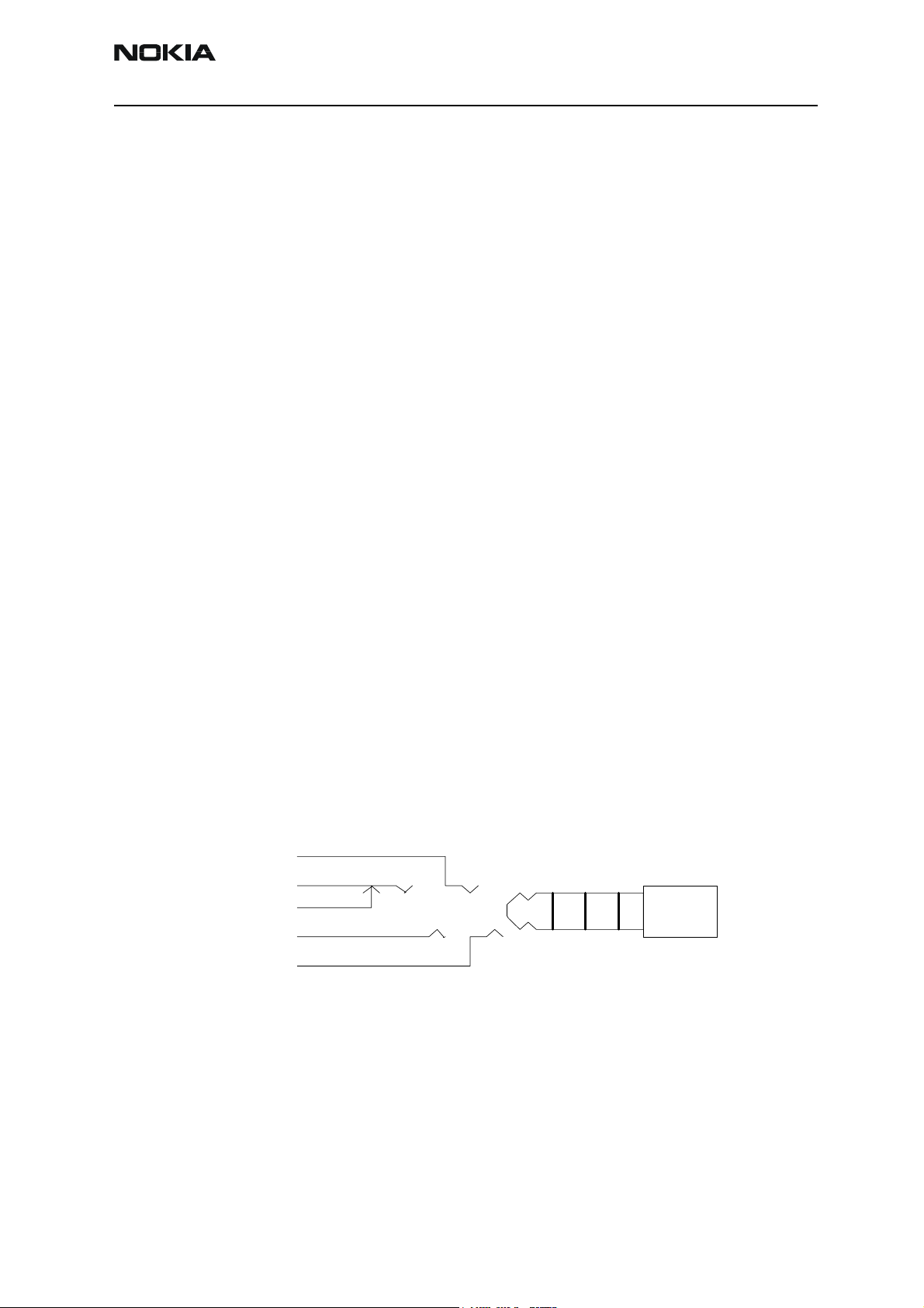
In RH-47, there is headset connector which is a fully differential 4–wire connection.
2. XEARN
4. XEARP
5. HE A D IN T
3. XM IC P
1. XM IC N
The handsfree (HF) driver in the UEM is meant for a headset. In RH-47, the output is
driven in fully differential mode. In the fully differential mode, the HF pin is the negative
output and HFCM pin is the positive output. The gain of the handsfree driver in the differential mode is 6 dB. The earpiece (EARP, EARN) and headset (HF, HFCM) signals are
multiplexed so that the outputs can not be used simultaneously. The HF and HFCM
amplifiers include a transient suppression circuitry.
Figure 5: External Audio Connector
The plug opens a mechanical switch inside the connector between HF and HeadInt lines.
The HeadInt line is pulled up to 2.7V by internal resistor when the switch is open. When
Issue 1 05/04 Copyright © 2004 Nokia Corporation Page 17
Company Confidential
Page 18
RH-47 Company Confidential
7 - Baseband Description & Troubleshooting Nokia Customer Care
the plug is not inserted, the voltage in the HeadInt line is <0.8 V caused by internal pull
down resistor in the HF line.
Flashing
SW download in service is implemented by custom tools and SW, kindly refer to Service
Software Instructions and Service Tools sections of the manual.
Testing interfaces
Testing interface electrical specifications
Pin Name Dir Parameter Min Typ Max Unit Notes
1 MBUS <->Vol 0 0.2 0.3*VFlash1 V
Vil (From Prommer) 0 0.2 0.3*VFlash1 V
Voh 0.7*VFlash1 2.7 0.7*VFlash1 V
Vih(From Prommer) 0.7*VFlash1 2.7 VFlash1 V
2 FBusTx -> Vol 0 2.7 0.3*VFlash1 V
Voh 0.7*VFlash1 2.7 VFlash1 V
3 FBusRx <- Vil (From Prommer) 0 2.7 0.3*VFlash1 V
Vih(FromPrommer) 1.89 2.7 VFlash1 V
Abs. Max. Voltage
to Test Pad Referenced to GND
4 VPP To Phone 0 / 2.8 / 12 +/-3%V Prommer
4 VPP To Phone 0 / 2.8 / 12 +/-3%V Prommer
5 GND 0 V VBAT
-0.3V 3.0 V Absolute Max
Voltage limits
to MBUS/
FBUS
4 VPP
Select
4 VPP
Select
GROUND
*Note: VFlash1 is 2.78 +/- 3%
Electrical Specifications for power supply interface in product testing
Pin Name Min Typ Max Unit Notes
1 VBAT 0 3.6 5.1 V
2 BSI 0 2.78 VFlash1 V Internal pullup
3 GND 0 V
Note: VAna & VFlash1 = 2.78 +/-3%
Page 18 Copyright © 2004 Nokia Corporation Issue 1 05/04
Company Confidential
Page 19

Company Confidential RH-47
Nokia Customer Care 6 - Baseband Description and Troubleshooting
Extreme voltages
Lithium-Ion battery BL-6C:
• Nominal voltage is 3.7V
• Lower extreme voltage is 2.8V (cut off voltage)
• Higher extreme voltage is 4.2V (charging high limit voltage)
Temperature conditions
Specifications are met within the range of –10C to +55C ambient temperature. Reduced
operation between [-30] and [+60]. Storage temperature range is of –40C to +85C.
Humidity and water resistance
Relative humidity range is 5 … 95%. Condensed or dripping water may cause intermittent malfunctions. Protection against dripping water have to be implemented in (enclosure) mechanics. Continuous dampness causes permanent damage to the module.
Issue 1 05/04 Copyright © 2004 Nokia Corporation Page 19
Company Confidential
Page 20

RH-47 Company Confidential
7 - Baseband Description & Troubleshooting Nokia Customer Care
Introduction to RH-47 Baseband Troubleshooting
This document is a guide for localizing and repairing electrical faults in the RH-47
device. First there is a brief guide for fault localizing. Then fault repairing is divided into
troubleshooting paths.
Before any service operation, you must be familiar with the RH-47 product and module
level architecture. You have to be also familiar with the RH-47 specific service tools such
as the Phoenix service software, flashing tools and software.
General guidelines for RH-47 troubleshooting
Tools needed for troubleshooting
• Service tools (as listed at service tools chapter in this service manual)
• Laboratory power supply with current indicator
• Oscilloscope
• Digital multimeter
General guidelines
If the device cannot be turned on by any means, see “dead device” troubleshooting.
Current consumption (missing consumption) gives an idea whether the device is able to
start up.
Dropping supply voltage or very large current consumption indicates a short circuit.
Check whether the connection with Phoenix works and what can be discovered with
Phoenix (ADC-readings, baseband self-test, BB-calibrations etc.).
If “CONTACT SERVICE” is shown on the display, check baseband self-tests with Phoenix.
Check visually display and rocker faults.
Force phone to LOCAL mode and make keyboard test with phoenix.
Check that the board-to-board connector is OK, and connectors make good contacts.
If there is a liquid damage, stop repairing!
If the fault is not obvious and Phoenix connection is OK, flash the phone before disassembling.
Disassemble phone: try to locate failed module.
When located, check the failed module visually:
Page 20 Copyright © 2004 Nokia Corporation Issue 1 05/04
Company Confidential
Page 21

Company Confidential RH-47
Nokia Customer Care 6 - Baseband Description and Troubleshooting
• Mechanical damages?
• Solder joints OK?
Continue with specific troubleshooting procedure for the module:
• If there is an obvious fault, repair it before reflashing the device.
• Flash first if a fault is not obvious.
• If flashing is not working go to flashing troubleshooting.
Due to CSP packages, short circuits or broken solder joints are not easily seen. If the
examined signal seems to be continuously low or high level, then measure for possible
short circuit to ground (signal low) or to supply voltage (signal high). Note that if a problem is not found from any visible contact/component, it can be under CSPs where the
signal is connected.
Care must be taken when assembling and disassembling the transceiver. Failure to do
this may result in unnecessary damage to the device.
Nominal current consumption
NOTE: service tools need some amount of current to work.
The following current consumption values are measured from a complete RH-47.
Vbatt = 3.6V
Measured nominal currents are drawn from the main battery.
Measurements have been made with a current probe connected to an oscilloscope.
Operating mode Current consumption
Idle 4.5-5mA
Local 50-55mA
Normal (display and keyb.LEDs on) 100-130mA
2W audio call 290mA
Issue 1 05/04 Copyright © 2004 Nokia Corporation Page 21
Company Confidential
Page 22

RH-47 Company Confidential
7 - Baseband Description & Troubleshooting Nokia Customer Care
Troubleshooting Paths
Dead or jammed device
Page 22 Copyright © 2004 Nokia Corporation Issue 1 05/04
Company Confidential
Page 23

Company Confidential RH-47
Nokia Customer Care 6 - Baseband Description and Troubleshooting
Partially damaged device
If the device is working, but some functionality is missing, try to localize where the problems is and see relevant part of this manual. For example, if audio is not working, see
“Audio Troubleshooting”, if charging is not working see “Charging troubleshooting”.
Most common symptoms reported by customer
This chapter describes the most common symptoms reported by customers when the
device is brought in for service. Some tips where the trouble can be found are also given.
When troubleshooting, use these tips and follow the given troubleshooting path.
Most common symptoms for audio problems
“Earpiece sound is missing”
”Handsfree sound is missing”
”Headset is not recognized”
”Microphone is not working”
”Volume cannot be adjusted”
”Ringing tones does not work”
”Audio volume too low”
See audio troubleshooting.
Most common symptoms for Bluetooth problems
”Bluetooth does not work or connection cannot be established”
Follow the Bluetooth troubleshooting guide lines gave relevant chapters.
Symptoms related to energy management
“Phone does not stay on”
”Charging is not working”
”Time is lost during battery change”
”Charging takes too long”
”Operating time is very short”
See relevant part of energy management troubleshooting
Problems related to UI module:
“UI-module keypad is not working”
”Rocker is not working”
”Backlight is dim”
”Backlight not even”
”Backlight is blinking”
”Keypad or display backlight is not working”
”Display related problems”
See UI module troubleshooting.
Issue 1 05/04 Copyright © 2004 Nokia Corporation Page 23
Company Confidential
Page 24

RH-47 Company Confidential
7 - Baseband Description & Troubleshooting Nokia Customer Care
Most common RF related symptoms:
“Call cannot be made”
”Phone does not find signal”
”Call is often dropped”
See RF troubleshooting
ASIC is changed
ASIC’s can be changed only at a defined service level.
Exchanged Component IMEI re-writing EM calibration RF tuning
D190 - UEM YES NO NO
D311 - Flash 1 YES YES YES
D312 - Flash 2 NO NO NO
D310 - SDRAM NO NO NO
D100 - UPP NO NO NO
N430 - BT MCM NO NO NO
Page 24 Copyright © 2004 Nokia Corporation Issue 1 05/04
Company Confidential
Page 25

Company Confidential RH-47
Nokia Customer Care 6 - Baseband Description and Troubleshooting
Test points
Test Point Signal Test point Signal Test point Signal
J109 UEMInt J204 AUXD J476 SIMRST (SIM reader)
J170 RFCLK_I J206 SLEEPX J477 VSIM
J190 EARDATA J260 VDD VCORE regulator J487 MMCDATA
J191 MICDATA J311 FLASH CE (D311) J488 MMCGND
J192 SIMIODAI J312 FLASH CE (D312) J490 MMCCLK
J193 SIMCLKI J334 Shutdown Audio PA J492 VMMC
J194 SIMIOCTRL J390 Current sense resistor J493 MMCGND
J195 MBUSTX J391 Current sense resistor J495 MMCCMD
J196 MBUSRX J392 Current sense resistor J497 MMCGND
J197 FBUSTXI J393 Current sense resistor
J198 FBUSRXI J470 SIMGND
J199 RFCONVCLK J471 SIMDATA (EMIF)
J200 RXID J472 SIMCLK (EMIF)
J201 RXQD J473 SIMRST (EMIF)
J202 TXID J474 SIMDATA (SIM reader)
J203 TXQD J475 SIMCLK (SIM reader)
Note! For test point locations, see Appendix A.
Issue 1 05/04 Copyright © 2004 Nokia Corporation Page 25
Company Confidential
Page 26

RH-47 Company Confidential
7 - Baseband Description & Troubleshooting Nokia Customer Care
“CONTACT SERVICE” on display
CONTACT SERVICE on display (self-tests by Phoenix)
Display information: “Contact Service”
This fault means that software is able to run and thus the watchdog of UEM can be
served.
Self-test functions are executed when the phone is powered on and if one or more selftest functions fail, the message “Contact Service” is shown on the display.
MCU self-test cases can be split into two categories: The ones that are executed during
power up and the ones that are executed only with a PC connected. These test and items
included are as follows:
If some of the self-tests failed, see relevant chapter in this troubleshooting document.
Page 26 Copyright © 2004 Nokia Corporation Issue 1 05/04
Company Confidential
Page 27

Company Confidential RH-47
Nokia Customer Care 6 - Baseband Description and Troubleshooting
1CK Baseband HW Subarea Troubleshooting
Flashing troubleshooting
RH-47 has two memory components installed on the main PWB. The best indication of
which one is causing problems can be obtained by flashing the device. It has to be kept
in mind that the two flashes are interfaced with UPP WD2 ASIC that might itself have
some problems. The necessary steps are described below. Phoenix error messages during
flashing greatly help on defining what is wrong. To be able to flash the device, most
device BB area components must function properly.
Flashing
faults
The phone does
not set Flashbus
TXD line high
after startup
No
The phone does
not set the
flashbus TXD
line low after the
startup
No
Memory
faults page
2
Yes
Yes
Measure BSI
pulse during
flash
programming
Is it ok?
Yes
Measure
FBUSTX line
during flash
programming is
it 1.8V?
Yes
No
Check connections
Check BB voltages
Check clocks
Change UEM
Check BSI line
Check BSI line
Battery connector, flex,
battery connector,
C381, R193, C231, C232, R200
No
C239, Z383, R384
Change
UEM
Change UPP
WD2
Issue 1 05/04 Copyright © 2004 Nokia Corporation Page 27
Company Confidential
Page 28

RH-47 Company Confidential
7 - Baseband Description & Troubleshooting Nokia Customer Care
Vpp resistor (R310)
Page 28 Copyright © 2004 Nokia Corporation Issue 1 05/04
Company Confidential
Page 29

Company Confidential RH-47
Nokia Customer Care 6 - Baseband Description and Troubleshooting
Energy management troubleshooting
Device does not stay on
If the device is switched off without any visible reason, there may be problems in the following areas:
• UEM watchdog problem (WD is not updated by SW)
• BSI line problem (BSI line is floating => contact failure)
• Battery line problem
• Soldering problem
The most likely reason is UEM WD (watchdog), which turns the device off after about 32
seconds if SW is jammed.
This may caused by SW problem, UPP_WD2 problem (Not server by SW), UEM or memory
malfunctions.
The following tests are recommended:
• General power checking
• Clocks
•Memory testing
• Serial Interface
If there is something wrong in the BSI line, the device seems to be dead after the power
key is pressed. However, the regulators of the device are on a few seconds before the
power down.
This mode can easily be detected from the current consumption of the device. After a
few seconds the current consumption drops almost to 0 mA.
In this case, check component or soldering:
• Battery connector X382
EMI-filter R381
UEM D190 (pin number C2)
If phone boots to TEST or LOCAL mode with normal battery, BSI is short circuited to
ground. Check EMI-filter and filtering capacitors, which are located in the BSI.
Issue 1 05/04 Copyright © 2004 Nokia Corporation Page 29
Company Confidential
Page 30

RH-47 Company Confidential
7 - Baseband Description & Troubleshooting Nokia Customer Care
General power checking
Use service tool SF-20. Battery voltage should be at least 3.6V. After phone disassembly,
use module jig MJ-21.
Page 30 Copyright © 2004 Nokia Corporation Issue 1 05/04
Company Confidential
Page 31

Company Confidential RH-47
Nokia Customer Care 6 - Baseband Description and Troubleshooting
Vcorea dead
Yes
Voltages at C262, C263
and L260 (both sides),
OK?
No
Retest
Yes
Change L260, OK? Retest
No
Check voltage at J260,
OK?
No
Change L261 and retest
Yes
Change N260 and
retest
Issue 1 05/04 Copyright © 2004 Nokia Corporation Page 31
Company Confidential
Page 32

RH-47 Company Confidential
7 - Baseband Description & Troubleshooting Nokia Customer Care
Power key troubleshooting
Phone cannot
be powered by
pressing pwr
key
Clocks troubleshooting
Clocks include the following:
• RF-clock
• DBUS, CBUS clocks
• Flash and SDRAM clocks
• Sleep clock
Connect
charger, phone
is powered
up?
Yes
Change power key
and retest
No
See dead device
troubleshooting
• Bluetooth clock
• SIM clock
• MMC clock
The main clock signal for the baseband is generated from the voltage controlled by crystal oscillator VCXO. This 26 MHz triangle wave clock signal is supplied to OSC_IN pin of
Mjoelner and out to UPPWD2. Inside UPPWD2 the clock frequency is divided into 13 MHz
Page 32 Copyright © 2004 Nokia Corporation Issue 1 05/04
Company Confidential
Page 33

Company Confidential RH-47
Nokia Customer Care 6 - Baseband Description and Troubleshooting
and then fed to RFBusClk.
In SLEEP mode the VCXO is off. UEM generates low frequency clock signal (32.768 kHz)
that is fed to UPP_WD2, Bluetooth and ZOCUS.
When the flashing of the device does not succeed, but powering is OK, follow these
instructions.
Note: The absence of clocks may indicate that the device (put phone to LOCAL mode
when the sleep is not allowed or press buttons so that phone is not in sleep mode) is in
sleep mode. Make sure that the device is not in sleep during clocks measuring.
IMPORTANT: Clock signals have to be measured with 1MΩ (or greater) probes!
Measure signal from J170. This should be 26Mhz clock signal. See Figure 2, “RFClk” on
the next page. For more information, see RF Troubleshooting.
Check that the crystal oscillator (B190) is oscillating at 32.768kHz frequency. If not,
change B190. If OK, measure sleepclk from PIN 26 BT module. Frequency should be the
same 32.678kHz (see Figure 6, “Sleep clock,” on page 34 below.) If not, change UEM.
Issue 1 05/04 Copyright © 2004 Nokia Corporation Page 33
Company Confidential
Page 34

RH-47 Company Confidential
7 - Baseband Description & Troubleshooting Nokia Customer Care
Figure 6: Sleep clock
Figure 7: RFClk
Page 34 Copyright © 2004 Nokia Corporation Issue 1 05/04
Company Confidential
Page 35

Company Confidential RH-47
Nokia Customer Care 6 - Baseband Description and Troubleshooting
Charging checking
Use the BL6-C battery and JBV-1 calibration set to test charging. (NOTE: power supply
cannot be charged if it not has a current sinking capability.) When you are charging a
totally empty battery, remember that start-up charging might take a bit longer than normally. During this time the display is blank.
If charger is not of NMP approved type and its current and voltage are not within NMP
charger window, software does not start charging and there is “NOT CHARGING” on the
display. Voltage should be between 5.3V - 9.5V and current between 200mA – 900mA
Remove and reconnect battery and charger a few times before you start to measure the
device. This check ensures that the fault really exists (refer to “Charging troubleshooting”).
Issue 1 05/04 Copyright © 2004 Nokia Corporation Page 35
Company Confidential
Page 36

RH-47 Company Confidential
7 - Baseband Description & Troubleshooting Nokia Customer Care
Figure 8: Charging troubleshooting
Check BL-6C, Btemp, BSI,
X382, R381, R390,
R200
Page 36 Copyright © 2004 Nokia Corporation Issue 1 05/04
Company Confidential
Page 37

Company Confidential RH-47
Nokia Customer Care 6 - Baseband Description and Troubleshooting
Nothing
happens
when ACP-8
is connected
Measure Vchar
at V380. Is it
>3.0Vdc?
Replace R190
and retest
Check F380, L380,
V380, C382, C389
Check R190,
is it OK?
Issue 1 05/04 Copyright © 2004 Nokia Corporation Page 37
Company Confidential
Page 38

RH-47 Company Confidential
7 - Baseband Description & Troubleshooting Nokia Customer Care
Energy management calibration
During energy management calibration, A/D-converter, BSI, Btemp, battery voltage,
charger voltage and charger current are calibrated.
Table 1: Limits for calculated calibration
Channel Low High
ADC Offset -50 50
ADC Gain 26000 29500
BSI Gain 860 1180
Vbatt Offset 2400 2600
Vbatt Gain 10000 11000
Vchar 57000 63000
Ichar 3600 5000
ADC-offset over limits:
Inspect the BSI line and components (R381, R200, pull-up resistor R193). If these are OK,
change UEM.
BSI Gain over limits:
Inspect the BSI line and components (R381, R200, pull-up resistor R193). If these are OK,
change UEM.
Page 38 Copyright © 2004 Nokia Corporation Issue 1 05/04
Company Confidential
Page 39

Company Confidential RH-47
Nokia Customer Care 6 - Baseband Description and Troubleshooting
Vbatt offset and Gain:
Inspect Vbatt lines and component in it.
Vchar over limits:
Inspect components which are connected to Vchar line: F380, L380 and V380.
Ichar over limits:
Inspect components which are connected to Vchar line. If those are OK, first change current sense resistor (R190). If calibration is still not successful, change UEM.
Calibration can be checked by using ADC-readings. Known voltages, currents and resistances are fed and read by ADC-readings, read values and known values can be compared.
ADC-reading
Divided and Scaled Battery Voltage, Charger Voltage, Charger Current, BSI and Btemp
values can be read by this tool. Read values a few times before you can be sure that the
results are accurate.
NOTE: If Vbatt Scaled and Divided unit results are different, default calibration values are
used. In this case perform EM calibration to get full performance of the phone.
Backup battery
A symptom of a backup battery fault is that the real time clock loses the correct time
during short main battery removal.
The same symptom can also be seen when the backup battery is empty. About 5 hours is
Issue 1 05/04 Copyright © 2004 Nokia Corporation Page 39
Company Confidential
Page 40

RH-47 Company Confidential
7 - Baseband Description & Troubleshooting Nokia Customer Care
needed to fully charge the backup battery in the device. NOTE: Backup battery is charged
only at the same time with main battery charging or when the device is in LOCAL or TEST
mode.
Always check the backup battery visually for any leakage or any other visual defect.
Check that the backup battery is correctly mounted in the device before closing the
cover.
Check with Phoenix that backup battery is OK.
Measure the voltage of backup battery:
• Normal operation when the voltage is > 2.0V
• Fully charged when the voltage is about 3.2V (because of large internal impedance voltage will not stay above 3.0V a long time after charging is disabled)
Enable backup battery charging (start to charge main battery or boot device to LOCAL or
TEST mode).
Measure voltage of backup battery during charging. It should arise, if it is not 3.2V, yet.
When the voltage is over 2.0V for sure, check backup battery with Phoenix.
-> If not OK, then D190 is faulty.
Ensure that the RTC is running.
Page 40 Copyright © 2004 Nokia Corporation Issue 1 05/04
Company Confidential
Page 41

Company Confidential RH-47
Nokia Customer Care 6 - Baseband Description and Troubleshooting
SIM card
The whole SIM interface is located in two chips UPP_WD2 and UEM. UEM contains the
SIM interface logic level shifting. UPP provides SIMClk through UEM to the SIM. SIM
interface supports both 3 V and 1.8 V SIMs.
UPP & UEM SIM connections
GND
UPP
SIM
C5 C6 C7
C1C2C3
BSI line from battery
SIMCLK
SIMRST
SIMDATA
VSIM
BSI
GND
UEM
SIMIF
register
SIMIO
SIMClk
Data
UEM
digital
logic
SIMIO
SIMClk
Data
UIF Block
UEMInt
CBusDa
CBusEnX
CBusClk
The SIM power up/down sequence is generated in the UEM. This means that the UEM
generates the RST signal to the SIM. Also the SIMCardDet signal is connected to the
UEM. The card detection is taken from the BSI signal, which detects the removal of the
battery. The monitoring of the BSI signal is done by a comparator inside the UEM. The
threshold voltage is calculated from the battery size specifications.
The SIM interface is powered up when the SIMCardDet signal indicates ”card in”. This
signal is derived from the BSI signal. SW tries first to power up the SIM with 1.8 V. If this
does not succeed, power up is repeated with VSIM switched to 3 V.
The data communication between the card and the phone is asynchronous half duplex.
The clock supplied to the card is in GSM system 1.083 MHz or 3.25 MHz. The data
baudrate is SIM card clock frequency divided by 372 (by default), 64, 32 or 16.
Issue 1 05/04 Copyright © 2004 Nokia Corporation Page 41
Company Confidential
Page 42

RH-47 Company Confidential
7 - Baseband Description & Troubleshooting Nokia Customer Care
Figure 9: SIM power-up sequence
Figure 10: SIM Clk 3.25MHz.
Remember to check the two Phoenix test cases before changing UPP!
Page 42 Copyright © 2004 Nokia Corporation Issue 1 05/04
Company Confidential
Page 43

Company Confidential RH-47
Nokia Customer Care 6 - Baseband Description and Troubleshooting
"Insert SIM Card" in device display, although the card is inserted
START
Perform
SIM BB self tests.
Are they OK?
Yes
Perform
Phoenix SIM tests.
Are they OK?
Yes
Is the SIM
Detection Reliable?
Yes
No
Check & clean battery
centre contact. Verify BSI
signal has a steady voltage.
Replace UEM
Perform
BB SIM self tests.
Are they OK?
Yes
Check SIM connector
Is it OK?
Yes
Measure VSIM.
Is it 1.8/3.0V when SIM
interface is powered
up?
Yes
NoNo
No
No
Replace UPP_WD2
Check & clean connector
contacts & pads
Replace connector
Measure VSIM
resistance to GND.
Is it low?
Yes
Check C470. Is it OK?
Yes
NoNo
No
Change UEM
Change VSIM
decoupler, C470
Problem solved?
Yes
END
No
Analyse signals & look for
errors in rise / fall times due
to wrong fitted / faulty
passives
Check SIM Power Up
sequencing. Is it OK?
Yes
No
Change SIM ASIP, R470
Check Clk, RST &
DATA at SIM connector.
Are the signals
present?
Yes
No
Check Clk,
RST & DATA between
UEM and the SIM ASIP.
Are the signals
present?
Yes
Change SIM ASIP, R470
No
Change UEM
Issue 1 05/04 Copyright © 2004 Nokia Corporation Page 43
Company Confidential
Page 44

RH-47 Company Confidential
7 - Baseband Description & Troubleshooting Nokia Customer Care
Audio troubleshooting
Figure 11: Internal earpiece
Page 44 Copyright © 2004 Nokia Corporation Issue 1 05/04
Company Confidential
Page 45

Company Confidential RH-47
Nokia Customer Care 6 - Baseband Description and Troubleshooting
Figure 12: Internal MIC
Issue 1 05/04 Copyright © 2004 Nokia Corporation Page 45
Company Confidential
Page 46

RH-47 Company Confidential
7 - Baseband Description & Troubleshooting Nokia Customer Care
Figure 13: External earpiece
Page 46 Copyright © 2004 Nokia Corporation Issue 1 05/04
Company Confidential
Page 47

Company Confidential RH-47
Nokia Customer Care 6 - Baseband Description and Troubleshooting
Figure 14: External MIC
Issue 1 05/04 Copyright © 2004 Nokia Corporation Page 47
Company Confidential
Page 48

RH-47 Company Confidential
7 - Baseband Description & Troubleshooting Nokia Customer Care
Figure 15: Internal MALT speaker
Page 48 Copyright © 2004 Nokia Corporation Issue 1 05/04
Company Confidential
Page 49

Company Confidential RH-47
Nokia Customer Care 6 - Baseband Description and Troubleshooting
Figure 16: Internal MALT speaker (2)
Issue 1 05/04 Copyright © 2004 Nokia Corporation Page 49
Company Confidential
Page 50

RH-47 Company Confidential
7 - Baseband Description & Troubleshooting Nokia Customer Care
Figure 17: Accessory detection
Page 50 Copyright © 2004 Nokia Corporation Issue 1 05/04
Company Confidential
Page 51

Company Confidential RH-47
Nokia Customer Care 6 - Baseband Description and Troubleshooting
Memory troubleshooting
Most memory related errors are found through flashing the device; flashing the device is
therefore recommended before any of the steps described in this chapter. Check flashing
troubleshooting section first!
There are however a few memory related errors that cannot be found through flashing.
• SDRAM(D310) partially damaged. This can mean that the SDRAM component
itself is partially damaged and all the memory locations cannot be successfully
read or there is a soldering problem somewhere either under UPP or SDRAM.
There is a BB self-test for testing SDRAM component quite thoroughly, but the
problem is that if SDRAM does not function properly one may not be able to run
those tests as SDRAM is used during the device boot and self-test cannot be run
if the device has not booted.
• DEVICE may inform about being "out of memory " more often than it should
• Flash1 (D312) is partially/totally damaged. During flashing the manufacturer,
device and revision IDs are read, but flashing is done based on IDs of the flash0
(D311). This means that one cannot see any error messages displayed on the
Phoenix window during flashing, if flash1 is failing. IDs are however displayed on
the Phoenix window and successful read of flash1 IDs can be checked from there.
Serial interface troubleshooting
CBUS
CBUS is a three wire serial interface between the main baseband components. The bus
consists of data, clock and bus_enable signals. In RH-47, the bus is connected from UPP
WD2 to ZOCUS, UEM and LPRF. UPP_WD2 takes care of controlling the traffic on the bus.
If the interface is faulty from the UPP WD2's end, the phone will not boot properly as
powering configurations do not work. Traffic on the bus can be monitored from three
pins on the BT module: pins 34, 35 and 36.
If however you are able to get the phone to boot up and can reach Phoenix BB self-tests
it is possible to test the functionality of each component attached to Cbus.
Use:
ST_ZOCUS_CBUS_IF_TEST to test AEM Cbus interface
ST_UEM_CBUS_IF_TEST to test UEM Cbus interface
ST_LPRF_IF_TEST to test Bluetooth Cbus interface
If an error is found testing any of the above components, you should replace the failing
component.
Issue 1 05/04 Copyright © 2004 Nokia Corporation Page 51
Company Confidential
Page 52

RH-47 Company Confidential
7 - Baseband Description & Troubleshooting Nokia Customer Care
FBUS
FBUS is a two wire RX and TX interface between UPP and flash/test interface. The bus
goes through UEM which adjusts the voltage levels to suit UPP_WD2. The interface voltage level on the phone flash/test pad pattern is 2.78V and on the UPP WD2 end it is 1.8V.
The functionality of this interface should not affect the device boot into NORMAL, LOCAL
or TEST modes. Phoenix tests can be performed through MBUS interface in the case of a
failure in FBUS interface. Flashing is not possible, if there is a problem in FBUS.
MBUS
MBUS is a two wire RX and TX interface between UPP and UEM. From UEM the interface
continues to flash/test interface as a one wire interface. UEM also adjusts the voltage
levels. The interface voltage level on the phone flash/test pad pattern is 2.78V and on the
UPP WD2 end it is 1.8V. MBUS traffic between UPP WD2 and UEM can be tested with
Phoenix (ST_MBUS_RX_TX_LOOP_TEST). Flashing is not possible, if there is a problem in
MBUS.
Page 52 Copyright © 2004 Nokia Corporation Issue 1 05/04
Company Confidential
Page 53

Company Confidential RH-47
Nokia Customer Care 6 - Baseband Description and Troubleshooting
Bluetooth troubleshooting
BT fault
Check BT202
soldering
Is soldering
bad?
No
Connection to
JBT9
Yes
Yes
Resolder or
replace the
module
BER
<=
0.1%
Check VAPPL pin
32
No
Is VAPPL OK? Check R435
Yes
Check SYSCLK
No
Does Vin=300-800
mVpp & Freq=26Mhz
No
Check buffer
section (V601)
Check Vcc pins
52, 53, 54
Is Vcc OK?
Yes
Is ripple <= 400
mVpp
Yes
No
No
Yes
BT OK
Check VBAT L431
Check VBAT 431
No
Yes
Replace BT202
module and flash
the phone
Check BER
BT OK
Yes
Check VREG pin 6
Is VREG OK?
Issue 1 05/04 Copyright © 2004 Nokia Corporation Page 53
Company Confidential
Page 54

RH-47 Company Confidential
7 - Baseband Description & Troubleshooting Nokia Customer Care
MMC troubleshooting
Page 54 Copyright © 2004 Nokia Corporation Issue 1 05/04
Company Confidential
Page 55

Company Confidential RH-47
Nokia Customer Care 6 - Baseband Description and Troubleshooting
Vibra
There may be three kinds of problems with the vibra:
• It does not rotate.
• It is noisy.
• it is continuously on.
Noisiness is usually caused by the contact of the rotating mass with surrounding
mechanics.
that C146 is
Check C145, C146,
C147
Issue 1 05/04 Copyright © 2004 Nokia Corporation Page 55
Company Confidential
Page 56

RH-47 Company Confidential
7 - Baseband Description & Troubleshooting Nokia Customer Care
ZOCUS
Check
N380
Page 56 Copyright © 2004 Nokia Corporation Issue 1 05/04
Company Confidential
Page 57

Company Confidential RH-47
Nokia Customer Care 6 - Baseband Description and Troubleshooting
UI Module Troubleshooting
This section describes the troubleshooting of the UI module
If the problem is in the display or in the keymat PWB, the entire UI module must be
replaced. However, the earpiece alone may be replaced (see audio troubleshooting).
Keymat backlight
If the keymat backlight is not functioning and the backlight driver voltage is generated
correctly on the 1CK module, then the problem is either in the connector or in the UI
Issue 1 05/04 Copyright © 2004 Nokia Corporation Page 57
Company Confidential
Page 58

RH-47 Company Confidential
7 - Baseband Description & Troubleshooting Nokia Customer Care
module. Note that it is possible that one LED is dead while all others are working.
Page 58 Copyright © 2004 Nokia Corporation Issue 1 05/04
Company Confidential
Page 59

Company Confidential RH-47
Nokia Customer Care 6 - Baseband Description and Troubleshooting
Keyboard problem
If the keyboard does not work, follow the troubleshooting chart below:
Change UPPWD2
Issue 1 05/04 Copyright © 2004 Nokia Corporation Page 59
Company Confidential
Page 60

RH-47 Company Confidential
7 - Baseband Description & Troubleshooting Nokia Customer Care
Display blank
Page 60 Copyright © 2004 Nokia Corporation Issue 1 05/04
Company Confidential
Page 61

Company Confidential RH-47
Nokia Customer Care 6 - Baseband Description and Troubleshooting
Backlight does not turn on
Issue 1 05/04 Copyright © 2004 Nokia Corporation Page 61
Company Confidential
Page 62

RH-47 Company Confidential
7 - Baseband Description & Troubleshooting Nokia Customer Care
Page 62 Copyright © 2004 Nokia Corporation Issue 1 05/04
Company Confidential
Page 63

Company Confidential RH-47
Nokia Customer Care 6 - Baseband Description and Troubleshooting
Appendix A
Test points - Bottom
Test points - Top
Issue 1 05/04 Copyright © 2004 Nokia Corporation Page 63
Company Confidential
Page 64

RH-47 Company Confidential
7 - Baseband Description & Troubleshooting Nokia Customer Care
[This page intentionally blank]
Page 64 Copyright© 2004 Nokia Corporation Issue 1 05/04
Company Confidential
 Loading...