

Page 1
9 - UI Schematics
Nokia Customer Care Schematics 1CJ_08 RH-47
Company Confidential
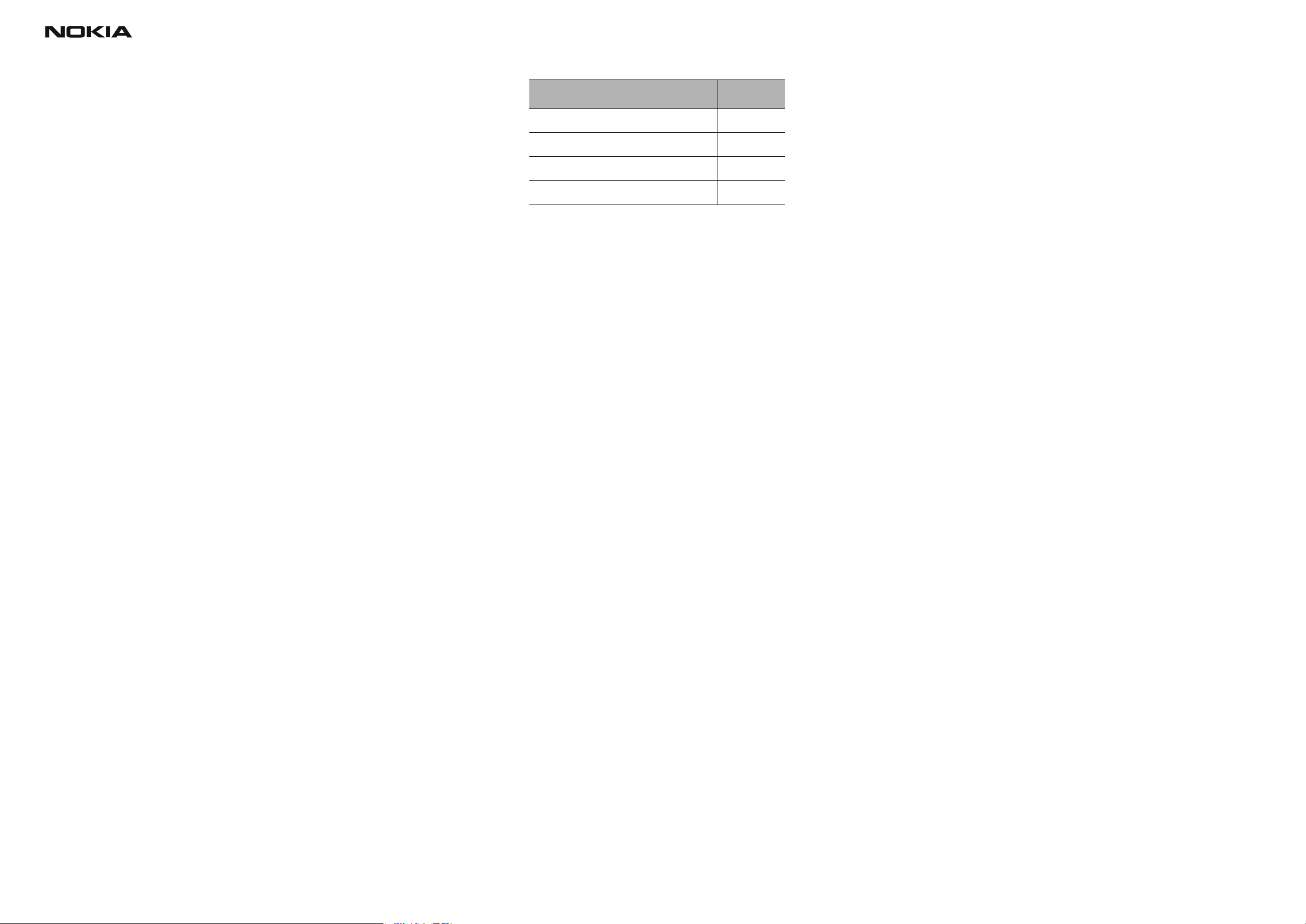
Table of Contents Page no.
User Interface v.0.0 ed. 59 2
User Interface v.0.0 ed. 54 3
Layout Diagram 1CJ_08, top 4
Layout Diagram 1CJ_08, bottom 5
Issue 1 05/04 © 2004 Nokia Corporation Page 1
Page 2
Nokia Customer Care Schematics 1CJ_08 RH-47
KLINGER dd-mKey User Interface 1
User Interface v.0.0 ed.59
V100
CL-191TD3-CD-T
CL-191TD3-CD-T
V101
CL-191TD3-CD-T
V102
CL-191TD3-CD-T
V103
V104
CL-191TD3-CD-T
CL-191TD3-CD-T
Company Confidential
V 100...104
X 100
R 100...123
C 100...102
B 100
J 100...101
V105
0
1
2
VBAT
PWR_EN
I2C_DA
GND
GND
--------------
Rows
--------------
Columns
--------------
X100
MATE
1
2
3
4
5
6
7
8
9
10
11
12
13
14
15
16
17
18
19
20
21
22
GND
B2B_Connector
GND
VKEYB
VBAT
PWR_EN
I2C_DA
I2C_CLK
I2C_INT
100R R104
VIO VIO
100R R107
100R
R105100R
R106100R
R108100R
R109
R110100R
14V/50V R112
GND
R11314V/50V
GND
14V/50V R114
GND
R11514V/50V
GND
14V/50V R116
GND
R117
14V/50V
14V/50V
GND GND
R118
I2C_CLK
3
GND
I2C_INT
4
GND
It must be possible to cut the GND track from connector pad
VIO
11
KEY_BUS(16:0)
0
1
2
3
4
5
5
6
4
7
3
8
2
9
1
10
0
11
12
4
13
3
14
2
15
1
16
0
Ear_0
Ear_1
C100
C101
22p
C102
GND
22p
22p
GND
R122
14V/50V
R123
14V/50V
GND
GND
J100
J101
B100
NA
NF
Name
Appr
Issue 1 05/04 © 2004 Nokia Corporation Page 2
Page 3

Nokia Customer Care Schematics 1CJ_08 RH-47
S100
S103
S102
S101
User Interface v.0.0 ed.54
Company Confidential
KEY_BUS(16:0)
NF
Shift
10
S104
1
8
S108
4
12
5 7
S112 S114
7
*
1413
5
S105
2
5
1314 6
S109
5 6
14
S113
8
#
7 9
12
S106
3
12
6
S110
8
9
Clear
0
Send
End
S107
S111
S115
13
13
7
1613
S116
NF
L-Soft
8
16
S118
R-Soft
14
10
S119
DRAFT
Up
10
S124 S125
S117
Appl
10
12
S120
DRAFT
1516
9
Dummy pads for production testing
Rocker key domes
DRAFT
Down
13 12
7
S121
9
16
S126
9
14
S123
S127
14
15
10
8 6
S122
DRAFT
SelectRight
9
12
Left
9
15
9
16 10
1510 16
Issue 1 05/04 © 2004 Nokia Corporation Page 3
Page 4

Nokia Customer Care Schematics 1CJ_08 RH-47
Layout diagram 1CJ_08, top
Company Confidential
Issue 1 05/04 © 2004 Nokia Corporation Page 4
Page 5

Nokia Customer Care Schematics 1CJ_08 RH-47
Layout diagram 1CJ_08, bottom
Company Confidential
Issue 1 05/04 © 2004 Nokia Corporation Page 5
Page 6

Nokia Customer Care Schematics 1CJ_08 RH-47
Company Confidential
Issue 1 05/04 © 2004 Nokia Corporation Page 6
 Loading...