

Page 1

Nokia Customer Care
RH-47 Series Cellular Phones
7 - RF Description and
Troubleshooting
Issue 1 05/04 Copyright © 2004 Nokia Corporation
Company Confidential
Page 2

RH-47 Company Confidential
1 - General Information Nokia Customer Care
[This page intentionally blank]
Page 2 Copyright© 2004 Nokia Corporation Issue 1 05/04
Company Confidential
Page 3

Company Confidential RH-47
Nokia Customer Care 7 - RF Description and Troubleshooting
Table of Contents
Page No
Abbreviations............................................................................................................................................ 5
Introduction to RF ................................................................................................................................... 6
RF power supply configuration .........................................................................................................9
General specifications of transceiver RH-47 ..............................................................................10
Introduction to RF Troubleshooting ................................................................................................ 11
Printed Wired Board ............................................................................................................................ 12
RF key component placement .........................................................................................................12
RF test points .......................................................................................................................................13
Test points RF supply voltages.................................................................................................... 14
RF test points Mjoelner chamber............................................................................................... 15
RF test points VCO chamber........................................................................................................ 15
RF test points PA chamber........................................................................................................... 16
Test points BB area......................................................................................................................... 16
Receiver Troubleshooting ................................................................................................................... 17
General instructions for RX troubleshooting ..............................................................................17
Measuring RX I/Q signals using RSSI reading ........................................................................ 17
Measuring RX performance using SNR measurement ......................................................... 18
Measuring front-end power levels using spectrum analyzer............................................. 20
Measuring analogue RX I/Q signals using oscilloscope....................................................... 21
Receiver troubleshooting .................................................................................................................22
Rx signal paths ....................................................................................................................................23
Antenna switch (RX/TX Switch).................................................................................................. 24
RX front-end .................................................................................................................................... 24
RX paths of Mjoelner RF ASIC..................................................................................................... 25
Transmitter ............................................................................................................................................. 26
General instructions for TX troubleshooting ..............................................................................26
TX signal paths ....................................................................................................................................26
Antenna switch (TX/RX switch) .................................................................................................. 28
GSM850 transmitter ..........................................................................................................................28
General instructions for GSM850 TX troubleshooting......................................................... 28
Troubleshooting for GSM850 transmitter ............................................................................... 29
GSM1900 (PCS) transmitter ............................................................................................................31
General instructions for GSM1900 TX troubleshooting ...................................................... 31
Troubleshooting for GSM1900 transmitter............................................................................. 32
Synthesizer ............................................................................................................................................. 35
General instructions for synthesizer troubleshooting ..............................................................35
Checking synthesizer operation .....................................................................................................35
26 MHz reference oscillator (VCXO) .............................................................................................36
VCO .........................................................................................................................................................37
Troubleshooting for PLL synthesizer .............................................................................................37
Frequency lists .....................................................................................................................................39
GSM850............................................................................................................................................. 39
GSM1900 .......................................................................................................................................... 40
DC Supply Current Check ................................................................................................................... 42
Phoenix Tunings after Repairs .......................................................................................................... 43
APPENDIX A: FLALI Test Cases with Hints for Repair................................................................. 44
APPENDIX B: FINUI Test Cases with Hints for Repair ................................................................ 50
Issue 1 05/04 Copyright © 2004 Nokia Corporation Page 3
Company Confidential
Page 4

Company Confidential RH-47
Nokia Customer Care 7 - RF Description and Troubleshooting
APPENDIX C: Component Placement with Test Points & Detailed Description.................. 59
APPENDIX D: Calibration of the DA-17/JXS-2 jig, Autotuning and BT Testing.................. 65
Requirements .......................................................................................................................................65
Calibration Problems .........................................................................................................................65
Active calibration: basic idea ..........................................................................................................65
Calibration procedure setup MJ-21 ..............................................................................................65
Data acquisition MJ-21 ....................................................................................................................66
MJ-21 TX power measurement ......................................................................................................67
MJ-21 GSM850 power measurement ..........................................................................................67
MJ-21 GSM1900 power measurement ........................................................................................68
MJ-21 receiver RSSI measurement ...............................................................................................68
MJ-21 RSSI procedure ......................................................................................................................68
MJ-21 RSSI values .............................................................................................................................69
MJ-21 example figures .....................................................................................................................70
JXS-2 / DA-17 “blackbox” setup ....................................................................................................70
Data acquisition JXS-2 / DA-17 .....................................................................................................70
DA-17/JXS-2 example figures ........................................................................................................71
Setting cable loss for Auto-Tuning ...............................................................................................71
Setting DA-17/JXS-2 calibration loss ...........................................................................................72
Assigning the product to the jig ....................................................................................................73
GPIB Setup for Autotuning ..............................................................................................................73
Autotuning ...........................................................................................................................................74
Bluetooth test setup ..........................................................................................................................75
Bluetooth testing ................................................................................................................................75
Issue 1 05/04 Copyright © 2004 Nokia Corporation Page 4
Company Confidential
Page 5

Company Confidential RH-47
Nokia Customer Care 7 - RF Description and Troubleshooting
Abbreviations
BB Baseband
PCS GSM1900
GSM GSM850
ESD Electro Static Discharge
GPRS General Packed Radio Service
HSCSD High Speed Circuit Switched Data
LNA Low Noise Amplifier
LO Local Oscillator
PA Power Amplifier
PWB Printed Wired Board
PLL Phase Locked Loop
RF Radio Frequency
RX Receiver
SA Spectrum Analyzer
TX Transmitter
VCO Voltage Controlled Oscillator
Issue 1 05/04 Copyright © 2004 Nokia Corporation Page 5
Company Confidential
Page 6

RH-47 Company Confidential
7 - RF Description and Troubleshooting Nokia Customer Care
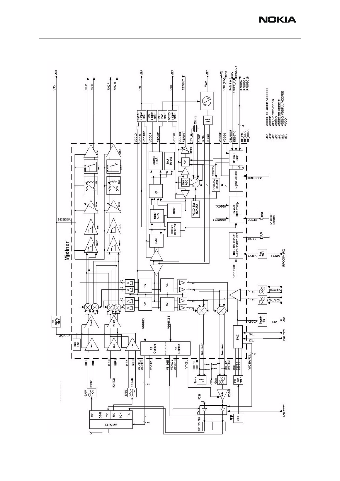
Introduction to RF
The RF front-end is a dual-band direct conversion transceiver. Using direct conversion, no
intermediate frequencies are used for up- or down -conversions.
The VCO oscillates on the doubled respectively quadruplicated frequency of the wanted
RX or TX frequency, depending on the band used. The VCO frequency is divided by either
2 or 4 and fed to the mixers (down-conversion) or modulators (up-conversion). Up- or
down-conversion is done in one step, directly between RF frequency and base band. All
up- and down-conversion takes place in the RF ASIC named Mjoelner (N601).
Mjoelner RF ASIC also contains PLL and LNAs for all used bands. ADC control section is
included to power and/or control GSM850 TX buffer, detector and antenna switch. The
Mjoelner RF ASIC is controlled via a serial bus.
Mjoelner RF ASIC contains an integrated VCXO which uses an external 26 MHz Xtal. No
analogue AFC signal is needed. AFC is realized via the serial interface port of Mjoelner.
The UPP is supplied by the 26 MHz reference clock of Mjoelner.
The phone supports GPRS (General Packet Radio Service), meaning multi-slot operation.
This will not require special equipment or procedures in repair situations.
The following diagrams show the RF frequency scheme and the RF block diagram.
Page 6 Copyright © 2004 Nokia Corporation Issue 1 05/04
Company Confidential
Page 7
Company Confidential RH-47
Nokia Customer Care 7 - RF Description and Troubleshooting
Figure 1: RF frequency scheme
869 - 894
MHz
1930 - 1990
MHz
F/4
F
FF
F/2
F
F/4F/2
PLL
26
MHz
3296
- 3980
MHz
X-
tal
I
RX
Q
26 MHz
BB clk
824 - 849
MHz
1850 - 1910
MHz
I
TX
Q
Mjoelner
Issue 1 05/04 Copyright © 2004 Nokia Corporation Page 7
Company Confidential
Page 8
RH-47 Company Confidential
7 - RF Description and Troubleshooting Nokia Customer Care
Figure 2: RF block diagram
Page 8 Copyright © 2004 Nokia Corporation Issue 1 05/04
Company Confidential
Page 9
Company Confidential RH-47
Nokia Customer Care 7 - RF Description and Troubleshooting
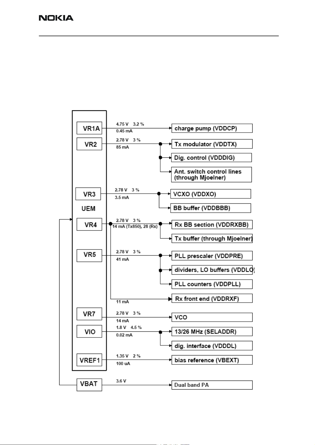
RF power supply configuration
All power supplies for the RF Unit are generated in the UEM IC (D190). All RF supplies
can be checked either in Mjoelner or in BB chamber.
The power supply configuration used is shown in the block diagram below. Values of
voltages are given as nominal outputs of UEM. Currents are typical values.
Figure 3: RF power distribution diagram
Issue 1 05/04 Copyright © 2004 Nokia Corporation Page 9
Company Confidential
Page 10
RH-47 Company Confidential
7 - RF Description and Troubleshooting Nokia Customer Care
General specifications of transceiver RH-47
Parameter Unit
Cellular System GSM850, GSM1900
RX Frequency Band GSM850: 869 … 894 MHz
GSM1900: 1930 … 1990 MHz
TX Frequency Band GSM850: 824 … 849 MHz
GSM1900: 1850 … 1910 MHz
Output Power GSM850: +5 … +33 dBm (3.2 mW … 2 W)
GSM1900: +0 … +30 dBm (1.0 mW … 1 W)
Duplex Spacing GSM850: 45 MHz
GSM1900: 80 MHz
Number of RF Channels GSM850: 124
GSM1900: 299
Channel Spacing 200 kHz (each band)
Number of TX Power Levels GSM850: 15
GSM1900: 16
Sensitivity, static channel GSM850: -102 dBm
GSM1900: -102 dBm
Frequency Error, static channel < 0.1 ppm
RMS Phase Error < 5.0 °
Peak Phase Error < |20.0 °|
Page 10 Copyright © 2004 Nokia Corporation Issue 1 05/04
Company Confidential
Page 11

Company Confidential RH-47
Nokia Customer Care 7 - RF Description and Troubleshooting
Introduction to RF Troubleshooting
This document shall provide instructions, how to check, repair and calibrate RH-47
phones. It is assumed, that the phones are disassembled and tested within a repair jig
MJ-21.
The following types of measurements have to be done for repair of the phone boards:
• RF measurements are made by using a Spectrum Analyzer together with a highfrequency probe (i.e. hp 85024A Note, that signal levels are not accurate ). Correct attenuation can be checked using a “good” phone board for example.
• LF (Low frequency) and DC measurements are made with an oscilloscope
together with a 10:1 probe.
• For receiver measurements a signal generator with frequencies up to 2000 MHz
is required. Most of the radio communication testers like CMD55 or CMU200 can
be used as signal generator. The signal generator is connected to the antenna
port using the repair jig MJ-21.
• Output level measurements of the transmitter are made with a power meter or a
calibrated spectrum analyser, which is connected to the antenna port using the
repair jig MJ-21.
Always make sure that the measurement set-up is calibrated when measuring RF parameters at the antenna port. Remember to include the correct losses of the module repair
jig and the connecting cable when realigning the phone.
Most RF semiconductors are static discharge sensitive. ESD protection must be taken
into account during repair (ground straps and ESD soldering irons).
Mjoelner RF ASIC is moisture sensitive. Therefore, Mjoelner RF ASIC must be pre-baked
prior to soldering.
Rx calibration done via Phoenix software is temperature sensitive because of calibration of the 26 MHz reference oscillator (VCXO). According to Mjoelner specification
ambient temperature has to be in a range from 22°C to 36°C.
Apart from key-components described in this document there are a lot of discrete components (resistors, inductors and capacitors) for which trouble shooting is done by
checking its proper soldering and complete assembly on the PWB. Capacitors and resistors can be checked by means of an LCR meter, but be aware in-circuit measurements
should be evaluated carefully.
In the following GSM850 will be used for the low band, and PCS or GSM1900 for the
high band.
Note: In this document there are example measurements being depicted with Phoenix Internal Service
Software A2003.42.1.48 pictures.
Issue 1 05/04 Copyright © 2004 Nokia Corporation Page 11
Company Confidential
Page 12
RH-47 Company Confidential
7 - RF Description and Troubleshooting Nokia Customer Care
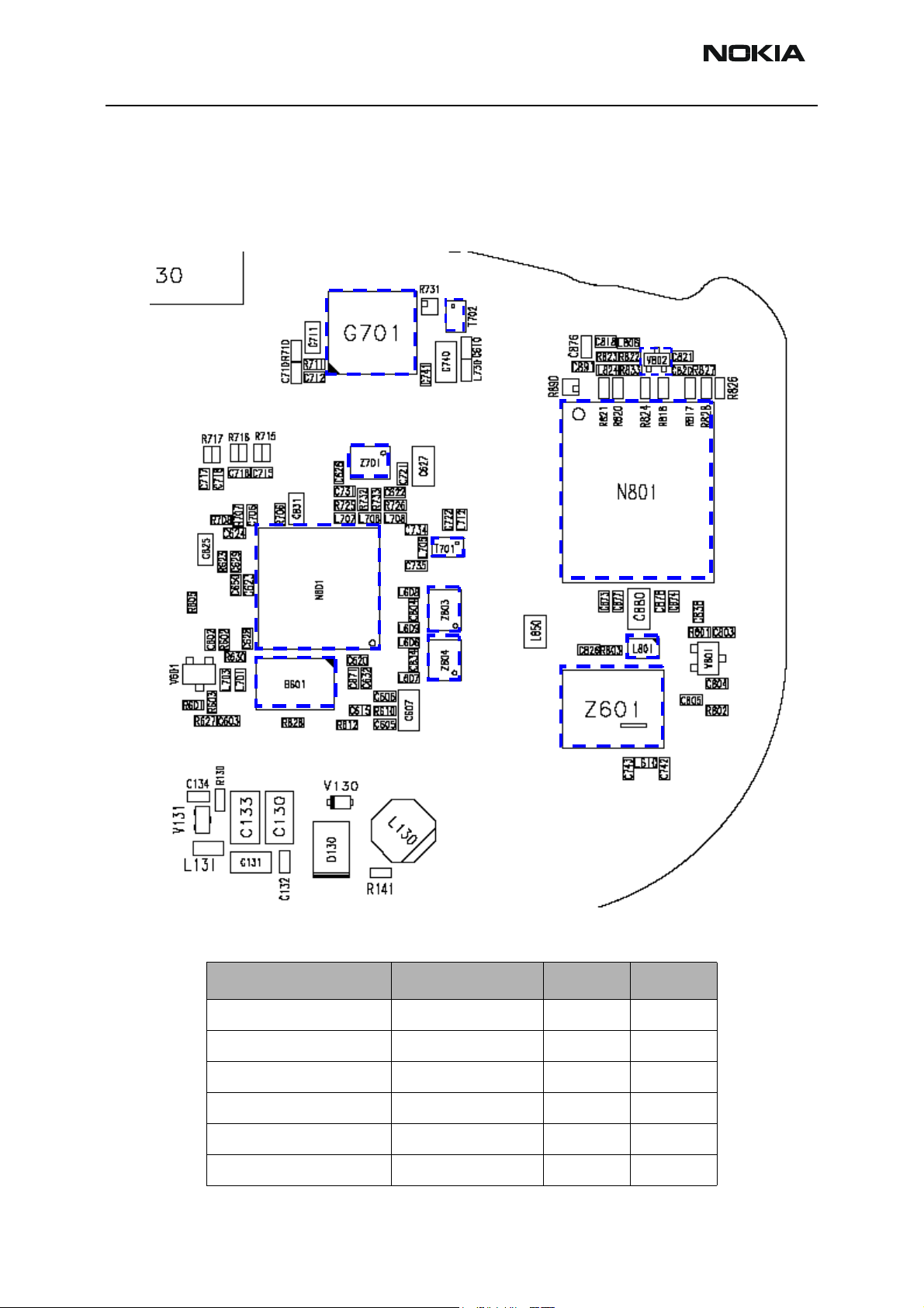
Printed Wired Board
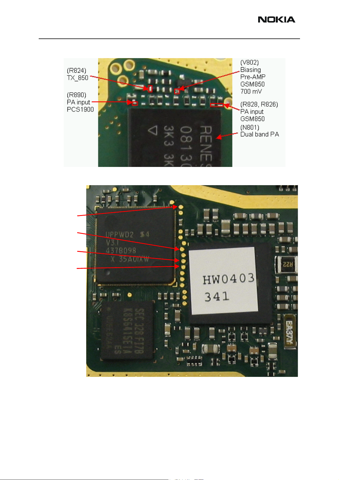
RF key component placement
Figure 4: RF key component placement
Description / Part Code Manufacturer’s code NMP Code Supplier
Dual band PA (N801) PF08130B-TB 4350403 Renesas
Mjölner RF ASIC F7 (N601) 4380013 Infineon
BT202i (N430) 0700085 Murata
UHF VCO (G701) ENFVJSW2S08 4350431 Matsushita
UHF VCO Balun (T702) LDB213G6010C-001 4550187 Murata
1900 Tx Balun (T701) LDB211G8005C-001 4550191 Murata
Page 12 Copyright © 2004 Nokia Corporation Issue 1 05/04
Company Confidential
Page 13
Company Confidential RH-47
Nokia Customer Care 7 - RF Description and Troubleshooting
1900 Rx SAW (Z603) 4511325 Murata
850 Tx SAW (Z701) 4511317 Murata
850 Rx SAW (Z604) 4511323 Murata
Antenna switch (Z601) LMZ0170 4510449 Murata
Crystal (B601) TSX-8A-25850 4510337 Toyocom
Tx Coupler (L801) LDC21836M19D-185 4550197 Murata
Tx850 buffer (V802) BFR949T-E6327 4210171 Infineon
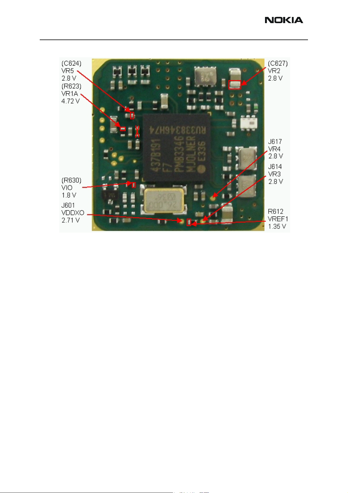
RF test points
The RF power supplies are generated in the UEM and can be measured either in the
Mjoelner chamber or in the base band chamber. On the drawing below small circles show
the locations of the test points.
Issue 1 05/04 Copyright © 2004 Nokia Corporation Page 13
Company Confidential
Page 14
RH-47 Company Confidential
7 - RF Description and Troubleshooting Nokia Customer Care
Test points RF supply voltages
Page 14 Copyright © 2004 Nokia Corporation Issue 1 05/04
Company Confidential
Page 15
Company Confidential RH-47
Nokia Customer Care 7 - RF Description and Troubleshooting
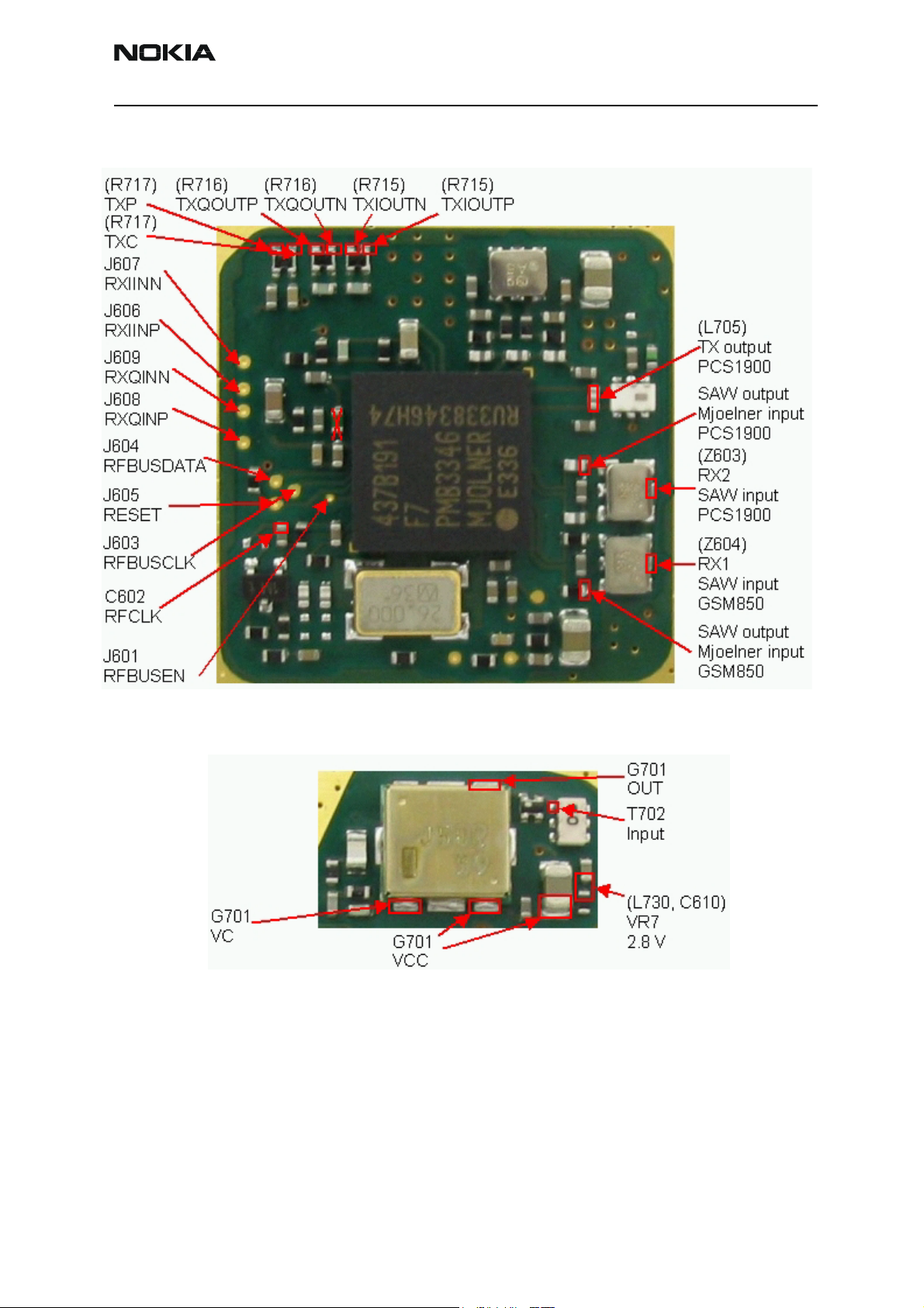
RF test points Mjoelner chamber
RF test points VCO chamber
Issue 1 05/04 Copyright © 2004 Nokia Corporation Page 15
Company Confidential
Page 16
RH-47 Company Confidential
7 - RF Description and Troubleshooting Nokia Customer Care
RF test points PA chamber
Test points BB area
J203 TXQD
J203 TXQD
J201 RXQD
J201 RXQD
J202 TXID
J202 TXID
J200 RXID
J200 RXID
Page 16 Copyright © 2004 Nokia Corporation Issue 1 05/04
Company Confidential
Page 17

Company Confidential RH-47
Nokia Customer Care 7 - RF Description and Troubleshooting
Receiver Troubleshooting
General instructions for RX troubleshooting
Connect the phone to a PC with Phoenix dongle PKD-1CS and DAU-9S cable (RS232).
Follow the instructions below.
Connect the phone to a power supply (DC voltage of 3.6V) and an RF signal generator.
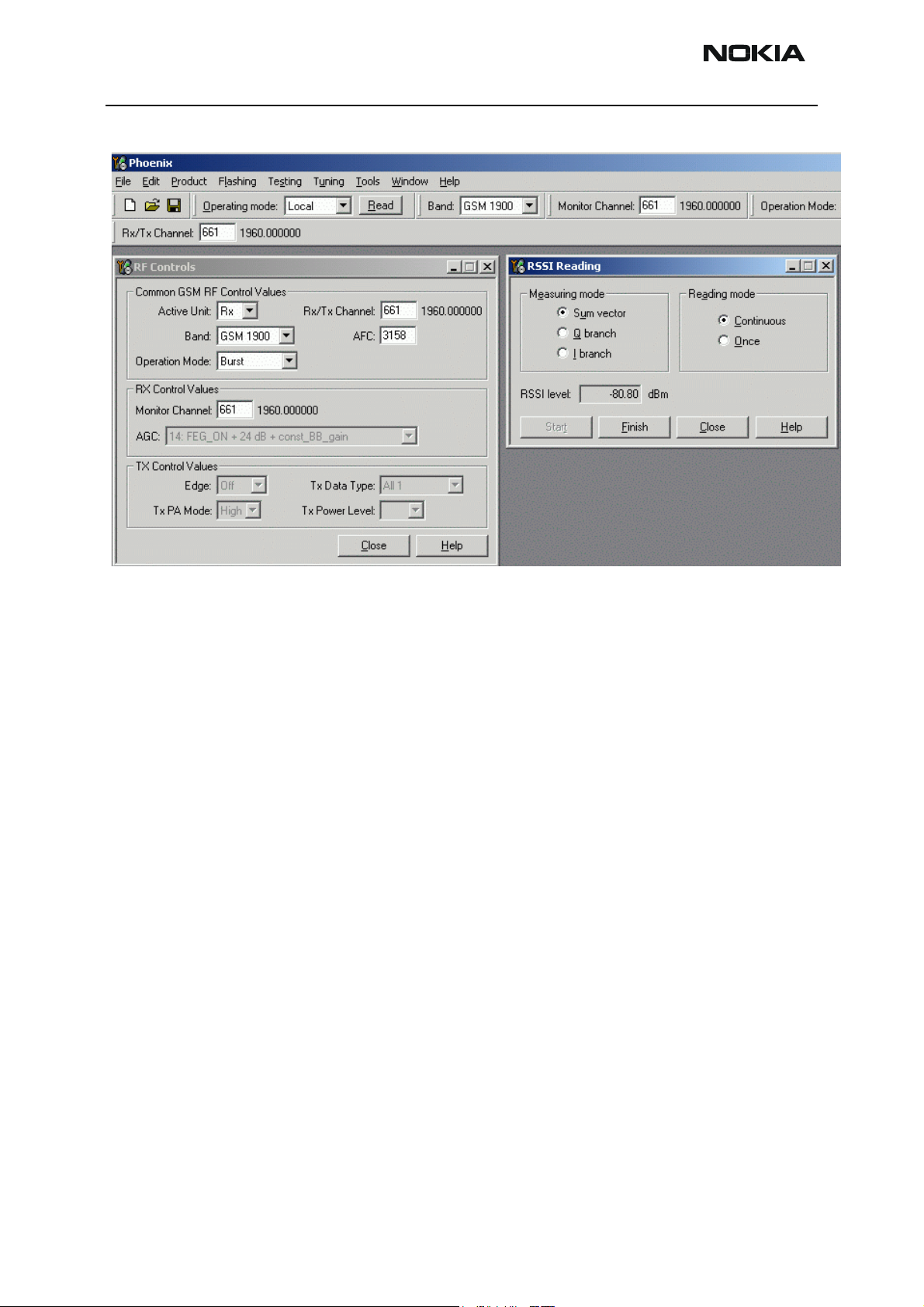
Measuring RX I/Q signals using RSSI reading
1 Start Phoenix Service Software and open FBUS connection:
Select Scan Product Ctrl-R
Wait until phone information is shown in the lower right corner of the screen.
2 Set operating mode to local mode:
Select Maintenance Alt-M
Testing T
RF Controls F
Wait until the RF Controls window pops up.
3 In the RF Controls window:
Select Band GSM850 or GSM1900
Active unit RX
Operation mode Burst
RX/TX Channel 190 or 661
Select Maintenance Alt-M
Testing T
RSSI reading R
Issue 1 05/04 Copyright © 2004 Nokia Corporation Page 17
Company Confidential
Page 18
RH-47 Company Confidential
7 - RF Description and Troubleshooting Nokia Customer Care
The setup should now look like this:
4 Make the following settings on your signal generator:
Frequencies:
GSM850: 881.66771 MHz (channel 190 + 67.710kHz offset)
GSM1900: 1960.06771 MHz(channel 661 + 67.710kHz offset)
RF power level:
– 80dBm @ the antenna connector of the phone (remembering to compensate for the cable and jig attenuation).
5 In RSSI reading, click Read now.
The resulting RSSI level should be – 80dBm +/– 0.5dB in each band.
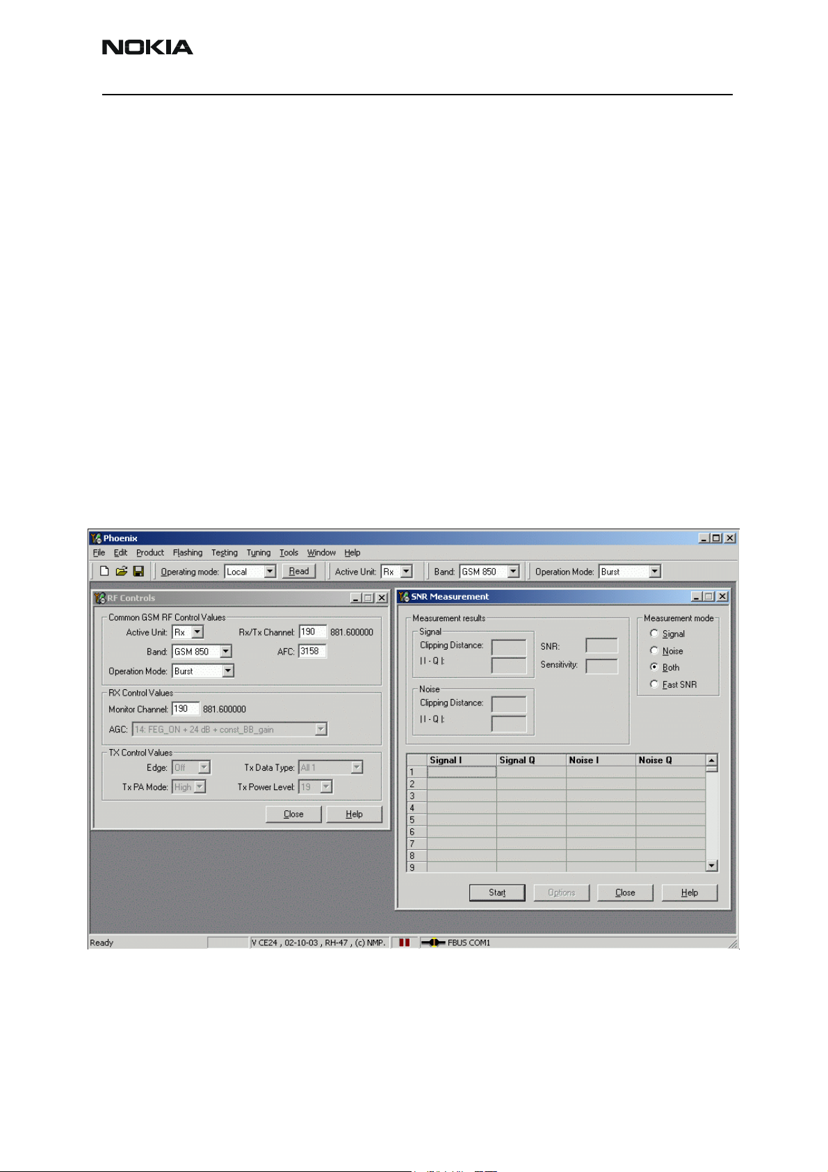
Measuring RX performance using SNR measurement
1 Start Phoenix Service Software and open FBUS connection.
Select Scan Product Ctrl-R
Wait until phone information is shown in the lower right corner of the screen.
2 Set operating mode to local mode.
Page 18 Copyright © 2004 Nokia Corporation Issue 1 05/04
Company Confidential
Page 19
Company Confidential RH-47
Nokia Customer Care 7 - RF Description and Troubleshooting
Select Maintenance Alt-M
Testing T
RF Controls F
Wait until the RF Controls window pops up.
3 In the RF Controls window:
Select Band GSM850 or GSM1900
Active unit RX
Operation mode Burst
RX/TX Channel 190 or 661
Select Maintenance Alt-M
Testing T
SNR Measurement M
Select Both (Radio Button)
The setup should now look like this:
4 Press the Start button.
5 To continue, follow the instructions in the following pop-up windows.
6 Connect an external signal generator to the RF connector of the phone and set
Issue 1 05/04 Copyright © 2004 Nokia Corporation Page 19
Company Confidential
Page 20
RH-47 Company Confidential
7 - RF Description and Troubleshooting Nokia Customer Care
the generator as instructed in the window. Take care for external cable and test
jig attenuation losses.
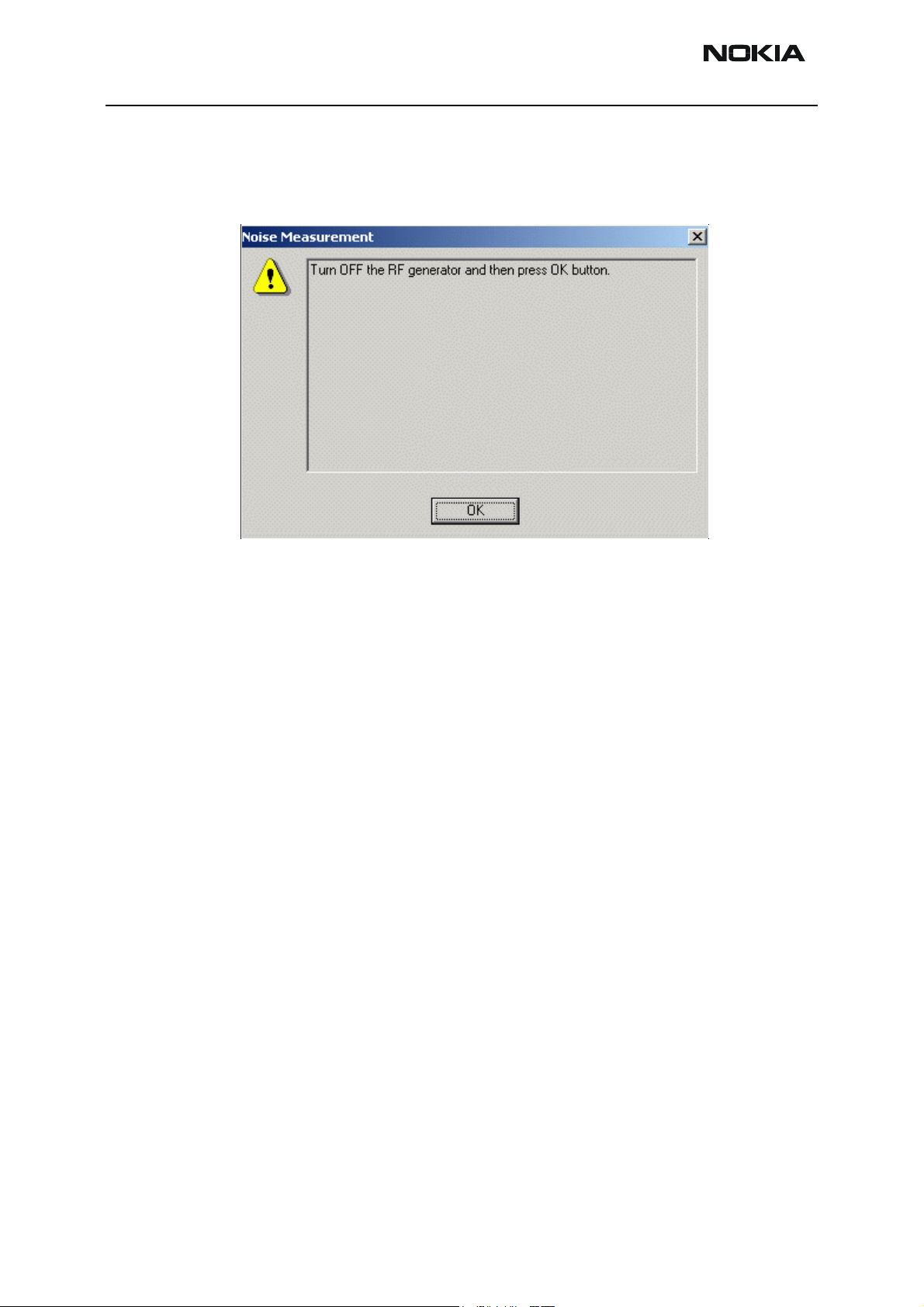
7 Switch off the external RF signal as instructed in the next pop-up window.
8 Press OK and read the SNR result.
The values should be:
GSM850 > 20dB
GSM1900 > 18dB
Measuring front-end power levels using spectrum analyzer
Spectrum Analyzer (SA) level values depend on the probe type and should be validated
using a good sample. The levels that are given here are measured using an hp 85024A
probe.
1 Start Phoenix Service Software and open FBUS connection:
Select Scan Product Ctrl-R
Wait until phone information is shown in the lower right corner of the screen.
2 Set operating mode to local mode:
Select Maintenance Alt-M
Testing T
RF Controls F
Wait until the RF Controls window pops up
3 In the RF Controls window:
Page 20 Copyright © 2004 Nokia Corporation Issue 1 05/04
Company Confidential
Page 21

Company Confidential RH-47
Nokia Customer Care 7 - RF Description and Troubleshooting
Select Band GSM850 or GSM1900
Active unit RX
Operation mode Continuous
RX/TX Channel 190 or 661
Please refer to the fault-finding chart and Appendix C for proper levels at different test
points.
Measuring analogue RX I/Q signals using oscilloscope
Measuring with an oscilloscope on “RXIINN” or “RXQINN” is recommended only if RSSI
reading does not provide enough information. There are dedicated test points for RX I
and Q signals. Apply an Input signal level of -80dBm.
1 Start Phoenix Service Software and open FBUS connection:
Select Scan Product Ctrl-R
Wait until phone information is shown in the lower right corner of the screen.
2 Set operating mode to local mode:
Select Maintenance Alt-M
Testing T
RF Controls F
Wait until the RF Controls window is pops up.
3 In the RF Controls window:
Select Band GSM850 or GSM1900
Active unit RX
Operation mode Continuous
RX/TX Channel 190 or 661
AGC 14
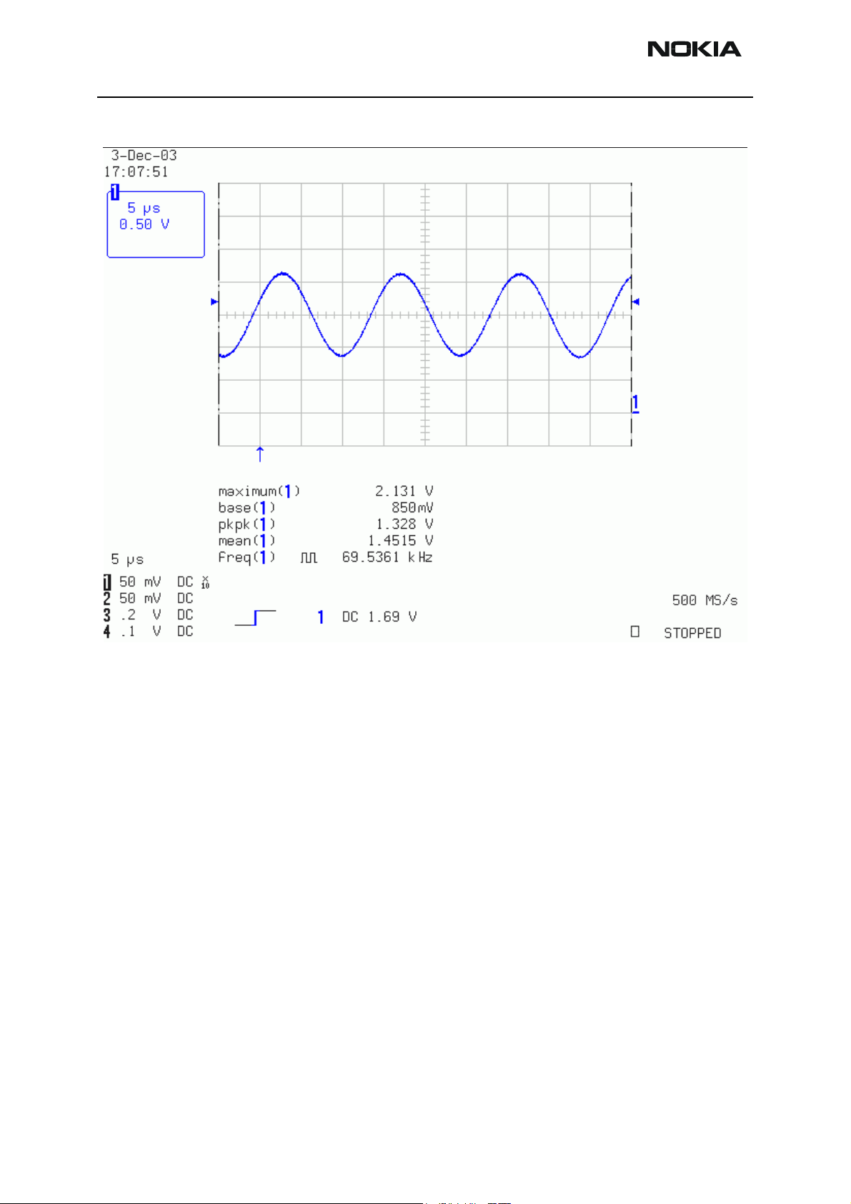
Following picture should be displayed on an oscilloscope' s screen if the GSM850
Issue 1 05/04 Copyright © 2004 Nokia Corporation Page 21
Company Confidential
Page 22
RH-47 Company Confidential
7 - RF Description and Troubleshooting Nokia Customer Care
receiver is working properly:
Receiver troubleshooting
The phone layout has dedicated test points for the analogue differential RX I and Q signals (RXIINP, RXIINN, RXQINP, RXQINN) from Mjoelner RF ASIC to UEM. The BB part is
used to measure those signals by means of RSSI reading. It is assumed that correct calibration of RSSI reading has been carried out in production.
RSSIreading [dBm] = 20log(U
Therefore, do not calibrate a defective phone before the phone error has been
found.
When a defective phone has been calibrated, a possible error in RX front-end might be
masked. In that case one can get a reasonable RSSI reading, although the front-end
shows excessive losses.
If you are not sure that incorrect re-calibration has been made, the following steps
should be done:
1 Check if AGC calibration is within limits.
) + AGC
BB
calibrated
Page 22 Copyright © 2004 Nokia Corporation Issue 1 05/04
Company Confidential
Page 23
Company Confidential RH-47
Nokia Customer Care 7 - RF Description and Troubleshooting
2 Check if SNR reading is OK.
Use an Oscilloscope to check levels of “RXIINN” and “RXQINN”.
Make sure that
Synthesiser
is working
Note: RF levels given in that chart are dependent on RF probe and m ust be v alidated with a known good sample
Apply -80dBm signal
from Generator
to Antenna Connector
phone: local, burst mode
GSM, PCS
RSSI reading
-80dBm
all bands
RX calibration
Calibration.
Rx chain
functional
= to be done in all 3 bands
?
within
limits
?
GSM, PCS
Apply -92dBm signal
No
Yes
from Generator
to Antenna Connector
phone: local, burst mode
SNR measurement
all bands
o.k.
?
Yes
No
Yes
= to be done in
defective band only
= to be done only once
(common for all bands)
No
wrong in both
Change signal level
to -60dBm
phone: local,
continous mode
Check
RxTx Switch
RSSI
and SN R
bands
?
SA
SA
Z601
Z601
Rx output
EGSMout
(850 &1900)
-76dBm
> -67dBm
?
No
Change
Z601
Yes
No
Yes
Check
SAW
Osci:
SA
RF-BB
Z601
serial
EGSMout
Interface
-76dBm
o.k.
?
No
BB Error
Check UPP
SA
SA
Z604,Z603
Z601
SAWout
EGSMout
both lines
-76dBm
>-72dBm
?
No
Change
Z604, Z603
Yes
Yes
EGSMout
Change
Mjolner
Check
Bias
C620, C632
Osci:
SA
RX I/Q
Z601
level
o.k.
-76dBm
?
No
Osci:
SA
LNA bias
Z601
(VR4)
EGSMout
=2.8V
-76dBm
?
Check
and
BB (UEM)
Yes
BB Error
Check UEM
Check
Bias
RX -BB bias
Yes
EGSMout
No
BB (UEM)
If RX and TX path seem to be faulty it has to be checked if the synthesizer is working. If
yes, then check the path from the antenna test pad J800 to the antenna switch Z601
(see RX troubleshooting "Check RXTX switch").
Osci:
SA
Z601
(VR4)
=2.8V
-76dBm
?
Check
C871
and
Check
Yes
LNA
No
Yes
Osci:
SA
LNA
Z601
base voltage
EGSMout
= 0.8V
-76dBm
?
No
Change
Mjoelner
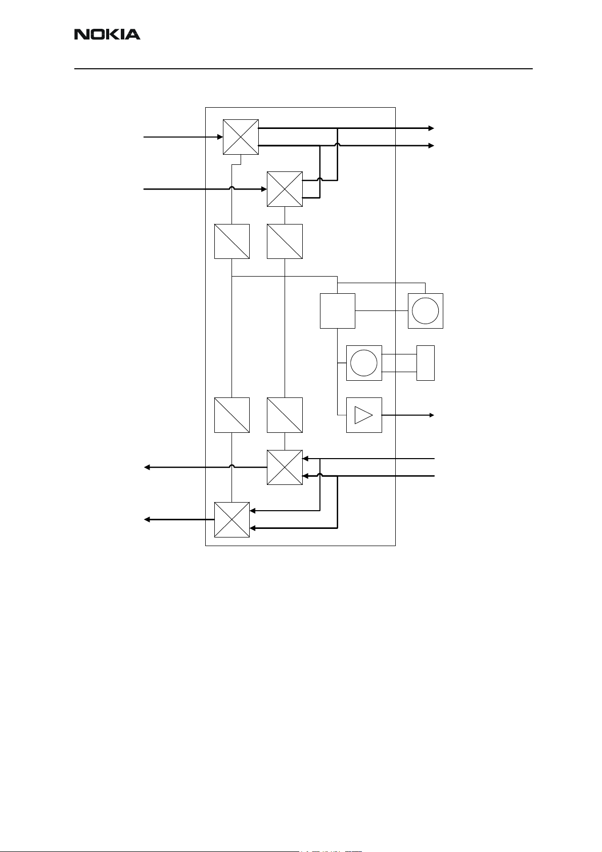
Rx signal paths
The signal paths of the receiver are shown in following block diagram. Note that the diagram shows GSM850 receiver (above) and the GSM1900 receiver (below).
Issue 1 05/04 Copyright © 2004 Nokia Corporation Page 23
Company Confidential
Page 24

RH-47 Company Confidential
7 - RF Description and Troubleshooting Nokia Customer Care
Figure 5: Rx signal paths
Rx
supply
filter
F
X
R
D
D
V
LNA
Bias
SAW
RX
GSM
TX
RX
Ant Switch
PCN
TX
2
RX850
RX1800
SAW
RX1900
INPL
LNA
INML
INPM
LNA
INMM
INPH
LNA
INMH
VANTL /
VANTM
2
VANTH
RF
Controls
RF
Controls
Pre-gain
Pre-gain
VDDDIG
VDDRXBB
222
2
1/2
BBAMP
BBAMP
1/4
B
B
X
R
D
D
V
BIQUAD
LPF1
LPF1
DCN1
DCN1
AGC
AGC
LPF2
BIQUAD
LPF2
DCN2
DCN2
VDDLO
Mjølner
VRX
RXIP
RXIM
RXQP
RXQM
VR6
Antenna switch (RX/TX Switch)
Signal path of RF: From the antenna-pad (J800) the RF signal is fed through the antenna
low pass filter (C743, L610, C748) to the antenna switch (Z601).
The antenna switch has the function of a diplexer which consists of two paths for
GSM850 and GSM1900. The GSM850 input signals pass the switch to the GSM_RX output. GSM1900 input signals pass to PCS_RX output. In receive mode both control signals
VC1 (VANTL) and VC2 (VANTH) have to be 0 V.
Signal paths:
GSM850: RX1-GSM output of the antenna switch Æ GSM850 SAW filter (Z604).
GSM1900: RX2-PCS output of the antenna switch Æ GSM1900 SAW filter (Z603).
The antenna switch including routed lines has following typical insertion losses:
GSM850: 1.3dB
GSM1900: 1.6dB
RX front-end
The RX front-end includes two SAW filters for GSM850 (Z604) and GSM1900 (Z603).
They are matched to the corresponding LNA inputs of Mjoelner RF ASIC (N601) with differential matching circuits (LC-type). The SAW filters provide out-of-band blocking
immunity. The integrated LNAs provide the front-end gains. Each of the SAW filters has a
single-ended input and a balanced output.
The SAW filters have maximum insertion losses of:
GSM850: 3.5dB
GSM1900: 4.0dB
Page 24 Copyright © 2004 Nokia Corporation Issue 1 05/04
Company Confidential
Page 25

Company Confidential RH-47
Nokia Customer Care 7 - RF Description and Troubleshooting
RX paths of Mjoelner RF ASIC
The balanced RX signal is amplified by the integrated LNA and the subsequent pre-gain
stage. After amplification the RX signal is down-converted.
The RX paths of Mjoelner RF ASIC consist of following sub units:
Separate LNAs for each of the two bands: GSM850 and GSM1900.
Two PRE-GAIN amplifiers, one for GSM850 and one for GSM1900.
Two passive I/Q mixers (MIX), one for GSM850 and one for GSM1900.
The BB signal paths consist of:
• Baseband amplifiers (BBAMP1). These amplifiers implement the initial channel
filtering.
• Low pass filters (LPF1).
• DC compensation / AGC amplifiers (DCN1). These amplifiers implement gain steps
from 0dB to 24dB in 6dB steps.
• Attenuators (AGC). They implement gain steps from -48dB to 0dB in 6dB steps,
yielding a total gain range of 72dB together with DCN1.
• Bi-quad filters (LPF2).
• DC compensation amplifiers (DCN2).
The differential base band outputs are internally DC-coupled and are connected directly
to the ADC inputs of the UEM-ASIC. The common mode level is set equal to the VBEXT
reference voltage.
Issue 1 05/04 Copyright © 2004 Nokia Corporation Page 25
Company Confidential
Page 26

RH-47 Company Confidential
7 - RF Description and Troubleshooting Nokia Customer Care
Transmitter
General instructions for TX troubleshooting
Connect an RF cable between the test jig and the measurement equipment (GSM test
equipment, power meter, spectrum analyzer, or similar).
Make use of an adequate attenuator at the input of your measurement equipment (10dB
to 20dB are recommended for a spectrum analyzer or a power meter). Assure not to
overload or destroy the equipment.
Connect the phone to a PC with DAU-9S cable (RS232) and Phoenix dongle PKD-1CS.
Provide the phone with power supply (3.6V).
Start Phoenix Service Software and open FBUS connection:
Select Scan Product Ctrl-R
and wait until phone information is shown in the lower right corner of the screen.
Follow the instructions in the chapters below.
TX signal paths
For easy error tracking it is important to know the signal paths of the transmitter. The
components are grouped in blocks and shown in the diagrams below.
Note that the diagram shows both GSM850 transmitter (below) and PCS1900 transmitter (above).
Page 26 Copyright © 2004 Nokia Corporation Issue 1 05/04
Company Confidential
Page 27

Company Confidential RH-47
A
A
A
A
Nokia Customer Care 7 - RF Description and Troubleshooting
Figure 6: Transmitter signal paths
VANTL / VANTH
3
3
3
3
VB_DET
VB_DET
VB_DET
VB_DET
VTXLOL
VTXLOL
VTXLOL
VTXLOL
VTXLOH
VTXLOH
VTXLOH
VTXLOH
VTXBH
VTXBH
VTXBH
VTXBH
VTXBL
VTXBL
VTXBL
VTXBL
PCN/PCS
PCN/PCS
PCN/PCS
PCS
PA
PA
PA
PA
DET
DET
DET
DET
VBATTRF
VBATTRF
VBATTRF
VBATTRF
Buffer
Buffer
Buffer
Buffer
GSM850
GSM850
GSM850
GSM850
PCS
PCS
PCS
PCS
TX
TX
TX
TX
n
n
n
n
t
t
t
t
S
S
S
S
GSM
GSM
GSM
GSM
wit
wit
wit
wit
TX
TX
TX
TX
Dir. Coupler
Dir. Coupler
Dir. Coupler
Dir. Coupler
Balun
Balun
Balun
Balun
VTX
VTX
VTX
VTX
SAW
SAW
SAW
SAW
PW-
PW-
PW-
PWloop
loop
loop
loop
filter
filter
filter
filter
OUTHP
OUTHP
OUTHP
OUTHP
OUTHM
OUTHM
OUTHM
OUTHM
OUTLP
OUTLP
OUTLP
OUTLP
OUTLM
OUTLM
OUTLM
OUTLM
DET
DET
DET
DET
PLFB1
PLFB1
PLFB1
PLFB1
PLFB2
PLFB2
PLFB2
PLFB2
VPCH/VPCL
VPCH/VPCL
VPCH/VPCL
VPCH/VPCL
RF
RF
RF
RF
RF
RF
Controls
Controls
Controls
Controls
Controls
Controls
RF
RF
RF
RF
RF
RF
Controls
Controls
Controls
Controls
Controls
Controls
Open
Open
Open
Open
Open
Open
collector
collector
collector
collector
collector
collector
Open
Open
Open
Open
Open
Open
collector
collector
collector
collector
collector
collector
2
2
2
2
P
P
P
P
TXP
TXP
TXP
TXP
PWC
PWC
PWC
PWC
PWC
PWC
TXCTX
TXCTX
TXCTX
TXCTX
TXC
TXC
TXC
TXC
VDDDIG
VDDDIG
VDDDIG
VDDDIG
VDDDIG
VDDDIG
VDDRXBB
VDDRXBB
VDDRXBB
VDDRXBB
V
V
V
V
D
D
D
D
DT
DT
DT
DT
Supply
Supply
Supply
Supply
filter
filter
filter
filter
VT
VT
VT
VT
X
X
X
X
VR2
VR2
VR2
VR2
1/4
1/4
1/4
1/4
1/4
1/4
1/2
1/2
1/2
1/2
1/2
1/2
2
2
2
2
2
2
2
2
2
2
2
2
2
2
2
2
TX
TX
TX
TX
Q
Q
Q
Q
P/
P/
P/
P/
TX
TX
TX
TX
Q
Q
Q
Q
2
2
2
2
2
2
2
2
2
2
2
2
Mjølner
Mjølner
Mjølner
Mjølner
2
2
2
2
TX
TX
TX
TX
IP/
IP/
IP/
IP/
TX
TX
TX
TX
IM
IM
IM
IM
The balanced TX IQ baseband signals (TXIOUTP, TXIOUTN, TXQOUTP, TXQOUTN) are provided by the baseband and are fed to the Mjoelner RF ASIC. The TX path of the Mjoelner
RF ASIC includes mainly two RF modulators for up-conversion of the baseband signals,
one for GSM850 and one for GSM1900. The baseband signal is up-converted with the LO
signal corresponding to the wanted TX channel. Both RF-TX outputs (850MHz and
1900MHz) of the Mjoelner RF ASIC are delivering balanced signals.
The GSM850 output signal of the Mjoelner RF ASIC is fed through the GSM TX SAW
filter (balanced to single ended) and the GSM850 MHz buffer to the GSM input of the
power amplifier (PA).
The GSM1900 output signal of the Mjoelner RF ASIC is fed through the TX balun (T701)
(balanced to single ended) and a 2dB pad to the GSM1900 input of the power amplifier
(PA).
The Dual Band PA has a maximum output power of approx. 35dBm at 850MHz and
33dBm at 1900MHz. DC-power supply is delivered directly from the battery through an
RF choke L850.
The RF output power is controlled by the power control loop. From the output of the PA
both signals are fed through a dual directional coupler (one of the power control loop
components) to the antenna switch.
Issue 1 05/04 Copyright © 2004 Nokia Corporation Page 27
Company Confidential
Page 28

RH-47 Company Confidential
7 - RF Description and Troubleshooting Nokia Customer Care
Antenna switch (TX/RX switch)
The antenna switch operates as a diplexer for the RX and TX signals. Moreover, it suppresses the TX harmonics generated by the PA. The antenna switch is controlled by the
Mjoelner RF ASIC using the control signals VC1 and VC2.
The following table shows the possible different states.
Table 1: Logic table for the antenna switching states
VC1 [Volt] VC2 [Volt] GSM RX PCS RX GSM TX PCS TX
0 0 X X
0 2.7 X
2.7 0 X
GSM850 transmitter
General instructions for GSM850 TX troubleshooting
Start the preparations as described in chapter General instructions for TX troubleshooting “General instructions for TX troubleshooting”.
1 Set operating mode to local mode.
Select Maintenance Testing RF Controls
Wait until the RF Controls window pops up.
2 In the RF Controls window:
Select Band GSM850
Active unit TX
Operation mode Burst
RX/TX Channel 190
TX Power Level 10
TX Data Type Random
Page 28 Copyright © 2004 Nokia Corporation Issue 1 05/04
Company Confidential
Page 29

Company Confidential RH-47
Nokia Customer Care 7 - RF Description and Troubleshooting
The setup should now look like this:
Now the measurement equipment should detect the following output signal of the
phone:
P
= +23 ± 1dBm @ 836.6 MHz
out
If this is not the case, then go to the next chapter for troubleshooting.
Troubleshooting for GSM850 transmitter
In the following troubleshooting chart, the TXP signal is used as a trigger-signal. For this
purpose a TXP test point is provided on the PWB, refer to figure RF test points in the
Mjoelner chamber.
Issue 1 05/04 Copyright © 2004 Nokia Corporation Page 29
Company Confidential
Page 30

RH-47 Company Confidential
7 - RF Description and Troubleshooting Nokia Customer Care
Use Phoenix to select
TX_Data Type: "1" or "0"
TX Power Level: 10
Yes
Oscilloscope
R612
C627
C717
C623
J614
Yes
Oscilloscope
R715
R715
R716
R716
Yes
Oscilloscope
R823
C641 (NF)
C640 (NF)
C803
Yes
Spectrum Analyzer No Check
R828 PA input PA Input
Compare with good
Yes Synthesizer
Use Phoenix to select
TX_Data Type: Random
TX Power Level: 10
Yes
Spectrum analyzer Check PA N801
L801 (B1_in) (PA N801
Pout_GSM)
Power >= +24 dBm, 836.6
MHz
Yes
Spectrum analyzer Check
RF-connector J800 No Directional Coupler
Pout
= +23 dBm, 836.6 MHz
Yes
GSM TX
OK
VREF1
VR2
TXP
VR5
VR3
TXIOUTP
Vdc = 1.35 Volt Check
Vdc = 2.78 Volt No Base Band
V = 1.8 Volt
Vdc = 2.78 Volt
Vdc = 2.78 Volt
67kHz
No Check
Vac = 0.4 Vpp, Vdc =
1.1 V
TXIOUTN
67kHz
Base Band
Vac = 0.4 Vpp, Vdc =
1.1 V
TXQOUTP
67kHz
Vac = 0.4 Vpp, Vdc =
1.1 V
TXQOUTN
67kHz
Vac = 0.4 Vpp, Vdc =
1.1 V
VTXB_850
VC1
Vdc = 2.78 Volt No Check:
Vdc = 0 Volt Mjoelner Serial
Interface
VC2
VBD
GSM850
Vdc = 2.78 Volt Mjoelner
Vdc = 2.78 Volt
P>= 5 dBm, 836.6 MHz
(with hp 85024A)
GSM TX SAW Filter
V802 Buffer
Mjoelner
sample
No Check Power Loop
L801,V801
Check TXC
(L801)
Antenna Switch (Z601)
LPF (C742,743,L610)
Page 30 Copyright © 2004 Nokia Corporation Issue 1 05/04
Company Confidential
Page 31

Company Confidential RH-47
Nokia Customer Care 7 - RF Description and Troubleshooting
GSM1900 (PCS) transmitter
General instructions for GSM1900 TX troubleshooting
Start the investigations as described in chapter General instructions for TX troubleshooting “General instructions for TX troubleshooting”.
1 Set operating mode to local mode:
Select Maintenance Testing RF Controls
Wait until the RF Controls window pops up.
2 In the RF Controls window:
Select Band GSM 1900
Active unit TX
Operation mode Burst
RX/TX Channel 661
TX Power Level 5
TX Data Type Random
The setup should now look like this:
Now the measurement equipment should detect the following output signal of the
phone:
= +20 ± 1dBm @ 1880MHz
P
out
If this is not the case, then go to the next chapter for troubleshooting.
Issue 1 05/04 Copyright © 2004 Nokia Corporation Page 31
Company Confidential
Page 32

RH-47 Company Confidential
7 - RF Description and Troubleshooting Nokia Customer Care
Troubleshooting for GSM1900 transmitter
In the following troubleshooting chart, the TXP signal is used as a trigger-signal. For this
purpose a TXP test point is provided on the PWB, refer to RF test points in the Mjoelner
chamber.
Page 32 Copyright © 2004 Nokia Corporation Issue 1 05/04
Company Confidential
Page 33

Company Confidential RH-47
Nokia Customer Care 7 - RF Description and Troubleshooting
Use Phoenix to select
TX_Data Type: "1" or "0"
TX Power Level: 5
Yes
Oscilloscope
R612
C627
C717
C623
J614
Yes
Oscilloscope
R715
R715
R716
R716
Yes
Oscilloscope
C641 (NF)
C649 (NF)
C803
Yes
Spectrum analyzer No Check
R819 in TX_1900 P>= 0 dBm, 1880 MHz DCS/PCS Balun
Mjoelner
Yes Synthesizer
Use Phoenix to select
TX_Data Type: Random
TX Power Level: 5
Yes
Spectrum analyzer Check PA N801
L809 (NF), B2_in (PA
N801 Pout_DCS)
Power = +22 dBm, 1880
MHz
Yes
Spectrum analyzer Check
RF-connector J800 No Directional Coupler
Pout =+20 dBm, 1880
MHz
Yes
PCS TX
OK
VREF01
VR2
TXP
VR5
VR3
TXIOUTP
Vdc = 1.35 Volt Check
Vdc = 2.78 Volt No Base Band
V = 1.8 Volt
Vdc = 2.78 Volt
Vdc = 2.78 Volt
67kHz
No Check
Vac = 0.4 Vpp, Vdc =
1.1 V
TXIOUTN
67kHz
Vac = 0.4 Vpp, Vdc =
Base Band
1.1 V
TXQOUTP
67kHz
Vac = 0.4 Vpp, Vdc =
1.1 V
TXQOUTN
67kHz
Vac = 0.4 Vpp, Vdc =
1.1 V
VC1
VC2
VDET
Vdc = 2.78 Volt Mjoelner Serial
Vdc = 2.78 Volt Mjoelner
Vdc = 2.78 Volt
No Check:
Interface
T701
No Check Power Loop
L801,V801
Check TXC
(L801)
Antenna Switch (Z601)
LPF (C742,743,L610)
Issue 1 05/04 Copyright © 2004 Nokia Corporation Page 33
Company Confidential
Page 34

RH-47 Company Confidential
7 - RF Description and Troubleshooting Nokia Customer Care
Figure 7: Example for TXP and TXC signal waveform (PCS1900 @ PL19)
Page 34 Copyright © 2004 Nokia Corporation Issue 1 05/04
Company Confidential
Page 35

Company Confidential RH-47
Nokia Customer Care 7 - RF Description and Troubleshooting
Synthesizer
One PLL synthesizer is generating all the required frequencies of both bands for Rx and
Tx. The VCO frequency is divided by 2 or by 4 in Mjoelner depending on the active band.
General instructions for synthesizer troubleshooting
Connect the phone to a PC with DAU-9S cable (RS232). The PC must have Phoenix Service Software installed and a PKD-1CS dongle is required.
Follow the instructions in the chapters below.
Checking synthesizer operation
1 Start Phoenix Service Software and open FBUS connection:
Select Scan Product Ctrl-R
Wait until phone information is shown in the lower right corner of the screen.
2 Set operating mode to local mode.
3 Start RF Control window:
Select Maintenance Alt-M
Tuning T
RF Controls F
Wait until the RF Controls window pops up.
4 Set the synthesizer to the following mode:
Select Band PCS1900
Active unit RX
Operation mode Continuous
RX/TX Channel 661
Issue 1 05/04 Copyright © 2004 Nokia Corporation Page 35
Company Confidential
Page 36

RH-47 Company Confidential
7 - RF Description and Troubleshooting Nokia Customer Care
The setup should now look like this:
The frequency of 3920MHz at the output of the VCO (G701) has to be measured with an
RF probe and a spectrum analyzer.
The tuning voltage can be easily measured at the VC input of the VCO (C712) The tuning
voltage should be 3.2 .. 3.4V at f
VCO
typically 240MHz/V.
If this is not the case, then go to chapter Troubleshooting for PLL synthesizer.
26 MHz reference oscillator (VCXO)
The VCXO is integrated in the Mjoelner RF-ASIC (N601). The only external component is
the 26MHz crystal (B601).
The reference oscillator has two functions:
• Reference frequency for the PLL synthesizer.
• System clock for BB (RFClk = 26 MHz).
For an error free initial synchronization, the 26MHz frequency of the VCXO must be
accurate enough. Therefore, a VCXO-calibration value is written via the serial Bus into
the RefOSCCAL register of Mjoelner and an additional bit in the RefOSCCntl register of
the Mjoelner. That is necessary for the rough calibration of the VCXO.
= 3920.0MHz. The tuning sensitivity of the VCO is
The VCXO is fine tuned by programming the AFC value via the serial bus of Mjoelner. The
Page 36 Copyright © 2004 Nokia Corporation Issue 1 05/04
Company Confidential
Page 37

Company Confidential RH-47
Nokia Customer Care 7 - RF Description and Troubleshooting
necessary AFC value is written into the RefOSCAFC register in Mjoelner.
VCO
The VCO is able to generate frequencies in the range of 3296.8 MHz to 3979.6 MHz
when the PLL is working properly. The frequency of the VCO signal is divided by 2 or by 4
in Mjoelner RF-ASIC. This allows the generation of all the frequencies in the GSM850
and the GSM1900 bands, both RX and TX.
The output frequency of the VCO is controlled by a DC voltage (VC) of the PLL loop filter.
The valid range of VC is 0.7V– 3.8V when the PLL is in steady state. The typical tuning
sensitivity is 240MHz/V. Even if the PLL is not working properly (VC outside the valid
range) a frequency at the output of the VCO can be detected between 3GHz and 4 GHz
(if the VCO itself is OK).
Troubleshooting for PLL synthesizer
It is important to note that the power supply of the VCXO (VR3) is only switched off in
the so-called ‘Deep Sleep Mode’ and the power supply of the VCO G701 (VR7) is switched
off in so-called ‘Sleep Mode’.
Issue 1 05/04 Copyright © 2004 Nokia Corporation Page 37
Company Confidential
Page 38

RH-47 Company Confidential
7 - RF Description and Troubleshooting Nokia Customer Care
Figure 8: PLL block diagram
Page 38 Copyright © 2004 Nokia Corporation Issue 1 05/04
Company Confidential
Page 39

Company Confidential RH-47
Nokia Customer Care 7 - RF Description and Troubleshooting
Frequency lists
GSM850
Channel TX RX TX VCO RX VCO Channel TX RX TX VCO RX VCO
128 824,2 869,2 3296,8 3476,8 190 836,6 881,6 3346,4 3526,4
129 824,4 869,4 3297,6 3477,6 191 836,8 881,8 3347,2 3527,2
130 824,6 869,6 3298,4 3478,4 192 837 882 3348 3528
131 824,8 869,8 3299,2 3479,2 193 837,2 882,2 3348,8 3528,8
132 825 870 3300 3480 194 837,4 882,4 3349,6 3529,6
133 825,2 870,2 3300,8 3480,8 195 837,6 882,6 3350,4 3530,4
134 825,4 870,4 3301,6 3481,6 196 837,8 882,8 3351,2 3531,2
135 825,6 870,6 3302,4 3482,4 197 838 883 3352 3532
136 825,8 870,8 3303,2 3483,2 198 838,2 883,2 3352,8 3532,8
137 826 871 3304 3484 199 838,4 883,4 3353,6 3533,6
138 826,2 871,2 3304,8 3484,8 200 838,6 883,6 3354,4 3534,4
139 826,4 871,4 3305,6 3485,6 201 838,8 883,8 3355,2 3535,2
140 826,6 871,6 3306,4 3486,4 202 839 884 3356 3536
141 826,8 871,8 3307,2 3487,2 203 839,2 884,2 3356,8 3536,8
142 827 872 3308 3488 204 839,4 884,4 3357,6 3537,6
143 827,2 872,2 3308,8 3488,8 205 839,6 884,6 3358,4 3538,4
144 827,4 872,4 3309,6 3489,6 206 839,8 884,8 3359,2 3539,2
145 827,6 872,6 3310,4 3490,4 207 840 885 3360 3540
146 827,8 872,8 3311,2 3491,2 208 840,2 885,2 3360,8 3540,8
147 828 873 3312 3492 209 840,4 885,4 3361,6 3541,6
148 828,2 873,2 3312,8 3492,8 210 840,6 885,6 3362,4 3542,4
149 828,4 873,4 3313,6 3493,6 211 840,8 885,8 3363,2 3543,2
150 828,6 873,6 3314,4 3494,4 212 841 886 3364 3544
151 828,8 873,8 3315,2 3495,2 213 841,2 886,2 3364,8 3544,8
152 829 874 3316 3496 214 841,4 886,4 3365,6 3545,6
153 829,2 874,2 3316,8 3496,8 215 841,6 886,6 3366,4 3546,4
154 829,4 874,4 3317,6 3497,6 216 841,8 886,8 3367,2 3547,2
155 829,6 874,6 3318,4 3498,4 217 842 887 3368 3548
156 829,8 874,8 3319,2 3499,2 218 842,2 887,2 3368,8 3548,8
157 830 875 3320 3500 219 842,4 887,4 3369,6 3549,6
158 830,2 875,2 3320,8 3500,8 220 842,6 887,6 3370,4 3550,4
159 830,4 875,4 3321,6 3501,6 221 842,8 887,8 3371,2 3551,2
160 830,6 875,6 3322,4 3502,4 222 843 888 3372 3552
161 830,8 875,8 3323,2 3503,2 223 843,2 888,2 3372,8 3552,8
162 831 876 3324 3504 224 843,4 888,4 3373,6 3553,6
163 831,2 876,2 3324,8 3504,8 225 843,6 888,6 3374,4 3554,4
164 831,4 876,4 3325,6 3505,6 226 843,8 888,8 3375,2 3555,2
165 831,6 876,6 3326,4 3506,4 227 844 889 3376 3556
166 831,8 876,8 3327,2 3507,2 228 844,2 889,2 3376,8 3556,8
167 832 877 3328 3508 229 844,4 889,4 3377,6 3557,6
168 832,2 877,2 3328,8 3508,8 230 844,6 889,6 3378,4 3558,4
169 832,4 877,4 3329,6 3509,6 231 844,8 889,8 3379,2 3559,2
170 832,6 877,6 3330,4 3510,4 232 845 890 3380 3560
171 832,8 877,8 3331,2 3511,2 233 845,2 890,2 3380,8 3560,8
172 833 878 3332 3512 234 845,4 890,4 3381,6 3561,6
173 833,2 878,2 3332,8 3512,8 235 845,6 890,6 3382,4 3562,4
174 833,4 878,4 3333,6 3513,6 236 845,8 890,8 3383,2 3563,2
175 833,6 878,6 3334,4 3514,4 237 846 891 3384 3564
176 833,8 878,8 3335,2 3515,2 238 846,2 891,2 3384,8 3564,8
177 834 879 3336 3516 239 846,4 891,4 3385,6 3565,6
178 834,2 879,2 3336,8 3516,8 240 846,6 891,6 3386,4 3566,4
179 834,4 879,4 3337,6 3517,6 241 846,8 891,8 3387,2 3567,2
180 834,6 879,6 3338,4 3518,4 242 847 892 3388 3568
181 834,8 879,8 3339,2 3519,2 243 847,2 892,2 3388,8 3568,8
182 835 880 3340 3520 244 847,4 892,4 3389,6 3569,6
183 835,2 880,2 3340,8 3520,8 245 847,6 892,6 3390,4 3570,4
184 835,4 880,4 3341,6 3521,6 246 847,8 892,8 3391,2 3571,2
185 835,6 880,6 3342,4 3522,4 247 848 893 3392 3572
186 835,8 880,8 3343,2 3523,2 248 848,2 893,2 3392,8 3572,8
187 836 881 3344 3524 249 848,4 893,4 3393,6 3573,6
188 836,2 881,2 3344,8 3524,8 250 848,6 893,6 3394,4 3574,4
189 836,4 881,4 3345,6 3525,6
251 848,8 893,8 3395,2 3575,2
Issue 1 05/04 Copyright © 2004 Nokia Corporation Page 39
Company Confidential
Page 40

RH-47 Company Confidential
GSM1900
7 - RF Description and Troubleshooting Nokia Customer Care
GSM1900
CH TX RX VCO TX VCO R X CH TX RX VCO TX VCO RX CH TX RX VCO TX V CO RX CH TX RX VCO TX VCO RX
512
1850,2 1930,2 3700,4 3860,4
513
1850,4 1930,4 3700,8 3860,8
514
1850,6 1930,6 3701,2 3861,2
515
1850,8 1930,8 3701,6 3861,6
516
1851,0 1931,0 3702,0 3862,0
517
1851,2 1931,2 3702,4 3862,4
518
1851,4 1931,4 3702,8 3862,8
519
1851,6 1931,6 3703,2 3863,2
520
1851,8 1931,8 3703,6 3863,6
521
1852,0 1932,0 3704,0 3864,0
522
1852,2 1932,2 3704,4 3864,4
523
1852,4 1932,4 3704,8 3864,8
524
1852,6 1932,6 3705,2 3865,2
525
1852,8 1932,8 3705,6 3865,6
526
1853,0 1933,0 3706,0 3866,0
527
1853,2 1933,2 3706,4 3866,4
528
1853,4 1933,4 3706,8 3866,8
529
1853,6 1933,6 3707,2 3867,2
530
1853,8 1933,8 3707,6 3867,6
531
1854,0 1934,0 3708,0 3868,0
532
1854,2 1934,2 3708,4 3868,4
533
1854,4 1934,4 3708,8 3868,8
534
1854,6 1934,6 3709,2 3869,2
535
1854,8 1934,8 3709,6 3869,6
536
1855,0 1935,0 3710,0 3870,0
537
1855,2 1935,2 3710,4 3870,4
538
1855,4 1935,4 3710,8 3870,8
539
1855,6 1935,6 3711,2 3871,2
540
1855,8 1935,8 3711,6 3871,6
541
1856,0 1936,0 3712,0 3872,0
542
1856,2 1936,2 3712,4 3872,4
543
1856,4 1936,4 3712,8 3872,8
544
1856,6 1936,6 3713,2 3873,2
545
1856,8 1936,8 3713,6 3873,6
546
1857,0 1937,0 3714,0 3874,0
547
1857,2 1937,2 3714,4 3874,4
548
1857,4 1937,4 3714,8 3874,8
549
1857,6 1937,6 3715,2 3875,2
550
1857,8 1937,8 3715,6 3875,6
551
1858,0 1938,0 3716,0 3876,0
552
1858,2 1938,2 3716,4 3876,4
553
1858,4 1938,4 3716,8 3876,8
554
1858,6 1938,6 3717,2 3877,2
555
1858,8 1938,8 3717,6 3877,6
556
1859,0 1939,0 3718,0 3878,0
557
1859,2 1939,2 3718,4 3878,4
558
1859,4 1939,4 3718,8 3878,8
559
1859,6 1939,6 3719,2 3879,2
560
1859,8 1939,8 3719,6 3879,6
561
1860,0 1940,0 3720,0 3880,0
562
1860,2 1940,2 3720,4 3880,4
563
1860,4 1940,4 3720,8 3880,8
564
1860,6 1940,6 3721,2 3881,2
565
1860,8 1940,8 3721,6 3881,6
566
1861,0 1941,0 3722,0 3882,0
567
1861,2 1941,2 3722,4 3882,4
568
1861,4 1941,4 3722,8 3882,8
569
1861,6 1941,6 3723,2 3883,2
570
1861,8 1941,8 3723,6 3883,6
606
1869,0 1949,0 3738,0 3898,0
607
1869,2 1949,2 3738,4 3898,4
608
1869,4 1949,4 3738,8 3898,8
609
1869,6 1949,6 3739,2 3899,2
610
1869,8 1949,8 3739,6 3899,6
611
1870,0 1950,0 3740,0 3900,0
612
1870,2 1950,2 3740,4 3900,4
613
1870,4 1950,4 3740,8 3900,8
614
1870,6 1950,6 3741,2 3901,2
615
1870,8 1950,8 3741,6 3901,6
616
1871,0 1951,0 3742,0 3902,0
617
1871,2 1951,2 3742,4 3902,4
618
1871,4 1951,4 3742,8 3902,8
619
1871,6 1951,6 3743,2 3903,2
620
1871,8 1951,8 3743,6 3903,6
621
1872,0 1952,0 3744,0 3904,0
622
1872,2 1952,2 3744,4 3904,4
623
1872,4 1952,4 3744,8 3904,8
624
1872,6 1952,6 3745,2 3905,2
625
1872,8 1952,8 3745,6 3905,6
626
1873,0 1953,0 3746,0 3906,0
627
1873,2 1953,2 3746,4 3906,4
628
1873,4 1953,4 3746,8 3906,8
629
1873,6 1953,6 3747,2 3907,2
630
1873,8 1953,8 3747,6 3907,6
631
1874,0 1954,0 3748,0 3908,0
632
1874,2 1954,2 3748,4 3908,4
633
1874,4 1954,4 3748,8 3908,8
634
1874,6 1954,6 3749,2 3909,2
635
1874,8 1954,8 3749,6 3909,6
636
1875,0 1955,0 3750,0 3910,0
637
1875,2 1955,2 3750,4 3910,4
638
1875,4 1955,4 3750,8 3910,8
639
1875,6 1955,6 3751,2 3911,2
640
1875,8 1955,8 3751,6 3911,6
641
1876,0 1956,0 3752,0 3912,0
642
1876,2 1956,2 3752,4 3912,4
643
1876,4 1956,4 3752,8 3912,8
644
1876,6 1956,6 3753,2 3913,2
645
1876,8 1956,8 3753,6 3913,6
646
1877,0 1957,0 3754,0 3914,0
647
1877,2 1957,2 3754,4 3914,4
648
1877,4 1957,4 3754,8 3914,8
649
1877,6 1957,6 3755,2 3915,2
650
1877,8 1957,8 3755,6 3915,6
651
1878,0 1958,0 3756,0 3916,0
652
1878,2 1958,2 3756,4 3916,4
653
1878,4 1958,4 3756,8 3916,8
654
1878,6 1958,6 3757,2 3917,2
655
1878,8 1958,8 3757,6 3917,6
656
1879,0 1959,0 3758,0 3918,0
657
1879,2 1959,2 3758,4 3918,4
658
1879,4 1959,4 3758,8 3918,8
659
1879,6 1959,6 3759,2 3919,2
660
1879,8 1959,8 3759,6 3919,6
661
1880,0 1960,0 3760,0 3920,0
662
1880,2 1960,2 3760,4 3920,4
663
1880,4 1960,4 3760,8 3920,8
664
1880,6 1960,6 3761,2 3921,2
700
1887,8 1967,8 3775,6 3935,6
701
1888,0 1968,0 3776,0 3936,0
702
1888,2 1968,2 3776,4 3936,4
703
1888,4 1968,4 3776,8 3936,8
704
1888,6 1968,6 3777,2 3937,2
705
1888,8 1968,8 3777,6 3937,6
706
1889,0 1969,0 3778,0 3938,0
707
1889,2 1969,2 3778,4 3938,4
708
1889,4 1969,4 3778,8 3938,8
709
1889,6 1969,6 3779,2 3939,2
710
1889,8 1969,8 3779,6 3939,6
711
1890,0 1970,0 3780,0 3940,0
712
1890,2 1970,2 3780,4 3940,4
713
1890,4 1970,4 3780,8 3940,8
714
1890,6 1970,6 3781,2 3941,2
715
1890,8 1970,8 3781,6 3941,6
716
1891,0 1971,0 3782,0 3942,0
717
1891,2 1971,2 3782,4 3942,4
718
1891,4 1971,4 3782,8 3942,8
719
1891,6 1971,6 3783,2 3943,2
720
1891,8 1971,8 3783,6 3943,6
721
1892,0 1972,0 3784,0 3944,0
722
1892,2 1972,2 3784,4 3944,4
723
1892,4 1972,4 3784,8 3944,8
724
1892,6 1972,6 3785,2 3945,2
725
1892,8 1972,8 3785,6 3945,6
726
1893,0 1973,0 3786,0 3946,0
727
1893,2 1973,2 3786,4 3946,4
728
1893,4 1973,4 3786,8 3946,8
729
1893,6 1973,6 3787,2 3947,2
730
1893,8 1973,8 3787,6 3947,6
731
1894,0 1974,0 3788,0 3948,0
732
1894,2 1974,2 3788,4 3948,4
733
1894,4 1974,4 3788,8 3948,8
734
1894,6 1974,6 3789,2 3949,2
735
1894,8 1974,8 3789,6 3949,6
736
1895,0 1975,0 3790,0 3950,0
737
1895,2 1975,2 3790,4 3950,4
738
1895,4 1975,4 3790,8 3950,8
739
1895,6 1975,6 3791,2 3951,2
740
1895,8 1975,8 3791,6 3951,6
741
1896,0 1976,0 3792,0 3952,0
742
1896,2 1976,2 3792,4 3952,4
743
1896,4 1976,4 3792,8 3952,8
744
1896,6 1976,6 3793,2 3953,2
745
1896,8 1976,8 3793,6 3953,6
746
1897,0 1977,0 3794,0 3954,0
747
1897,2 1977,2 3794,4 3954,4
748
1897,4 1977,4 3794,8 3954,8
749
1897,6 1977,6 3795,2 3955,2
750
1897,8 1977,8 3795,6 3955,6
751
1898,0 1978,0 3796,0 3956,0
752
1898,2 1978,2 3796,4 3956,4
753
1898,4 1978,4 3796,8 3956,8
754
1898,6 1978,6 3797,2 3957,2
755
1898,8 1978,8 3797,6 3957,6
756
1899,0 1979,0 3798,0 3958,0
757
1899,2 1979,2 3798,4 3958,4
758
1899,4 1979,4 3798,8 3958,8
794
1906,6 1986,6 3813,2 3973,2
795
1906,8 1986,8 3813,6 3973,6
796
1907,0 1987,0 3814,0 3974,0
797
1907,2 1987,2 3814,4 3974,4
798
1907,4 1987,4 3814,8 3974,8
799
1907,6 1987,6 3815,2 3975,2
800
1907,8 1987,8 3815,6 3975,6
801
1908,0 1988,0 3816,0 3976,0
802
1908,2 1988,2 3816,4 3976,4
803
1908,4 1988,4 3816,8 3976,8
804
1908,6 1988,6 3817,2 3977,2
805
1908,8 1988,8 3817,6 3977,6
806
1909,0 1989,0 3818,0 3978,0
807
1909,2 1989,2 3818,4 3978,4
808
1909,4 1989,4 3818,8 3978,8
809
1909,6 1989,6 3819,2 3979,2
810
1909,8 1989,8 3819,6 3979,6
Page 40 Copyright © 2004 Nokia Corporation Issue 1 05/04
Company Confidential
Page 41

Company Confidential RH-47
Nokia Customer Care 7 - RF Description and Troubleshooting
570
1861,8 1941,8 3723,6 3883,6
571
1862,0 1942,0 3724,0 3884,0
572
1862,2 1942,2 3724,4 3884,4
573
1862,4 1942,4 3724,8 3884,8
574
1862,6 1942,6 3725,2 3885,2
575
1862,8 1942,8 3725,6 3885,6
576
1863,0 1943,0 3726,0 3886,0
577
1863,2 1943,2 3726,4 3886,4
578
1863,4 1943,4 3726,8 3886,8
579
1863,6 1943,6 3727,2 3887,2
580
1863,8 1943,8 3727,6 3887,6
581
1864,0 1944,0 3728,0 3888,0
582
1864,2 1944,2 3728,4 3888,4
583
1864,4 1944,4 3728,8 3888,8
584
1864,6 1944,6 3729,2 3889,2
585
1864,8 1944,8 3729,6 3889,6
586
1865,0 1945,0 3730,0 3890,0
587
1865,2 1945,2 3730,4 3890,4
588
1865,4 1945,4 3730,8 3890,8
589
1865,6 1945,6 3731,2 3891,2
590
1865,8 1945,8 3731,6 3891,6
591
1866,0 1946,0 3732,0 3892,0
592
1866,2 1946,2 3732,4 3892,4
593
1866,4 1946,4 3732,8 3892,8
594
1866,6 1946,6 3733,2 3893,2
595
1866,8 1946,8 3733,6 3893,6
596
1867,0 1947,0 3734,0 3894,0
597
1867,2 1947,2 3734,4 3894,4
598
1867,4 1947,4 3734,8 3894,8
599
1867,6 1947,6 3735,2 3895,2
600
1867,8 1947,8 3735,6 3895,6
601
1868,0 1948,0 3736,0 3896,0
602
1868,2 1948,2 3736,4 3896,4
603
1868,4 1948,4 3736,8 3896,8
604
1868,6 1948,6 3737,2 3897,2
605
1868,8 1948,8 3737,6 3897,6
664
1880,6 1960,6 3761,2 3921,2
665
1880,8 1960,8 3761,6 3921,6
666
1881,0 1961,0 3762,0 3922,0
667
1881,2 1961,2 3762,4 3922,4
668
1881,4 1961,4 3762,8 3922,8
669
1881,6 1961,6 3763,2 3923,2
670
1881,8 1961,8 3763,6 3923,6
671
1882,0 1962,0 3764,0 3924,0
672
1882,2 1962,2 3764,4 3924,4
673
1882,4 1962,4 3764,8 3924,8
674
1882,6 1962,6 3765,2 3925,2
675
1882,8 1962,8 3765,6 3925,6
676
1883,0 1963,0 3766,0 3926,0
677
1883,2 1963,2 3766,4 3926,4
678
1883,4 1963,4 3766,8 3926,8
679
1883,6 1963,6 3767,2 3927,2
680
1883,8 1963,8 3767,6 3927,6
681
1884,0 1964,0 3768,0 3928,0
682
1884,2 1964,2 3768,4 3928,4
683
1884,4 1964,4 3768,8 3928,8
684
1884,6 1964,6 3769,2 3929,2
685
1884,8 1964,8 3769,6 3929,6
686
1885,0 1965,0 3770,0 3930,0
687
1885,2 1965,2 3770,4 3930,4
688
1885,4 1965,4 3770,8 3930,8
689
1885,6 1965,6 3771,2 3931,2
690
1885,8 1965,8 3771,6 3931,6
691
1886,0 1966,0 3772,0 3932,0
692
1886,2 1966,2 3772,4 3932,4
693
1886,4 1966,4 3772,8 3932,8
694
1886,6 1966,6 3773,2 3933,2
695
1886,8 1966,8 3773,6 3933,6
696
1887,0 1967,0 3774,0 3934,0
697
1887,2 1967,2 3774,4 3934,4
698
1887,4 1967,4 3774,8 3934,8
699
1887,6 1967,6 3775,2 3935,2
758
1899,4 1979,4 3798,8 3958,8
759
1899,6 1979,6 3799,2 3959,2
760
1899,8 1979,8 3799,6 3959,6
761
1900,0 1980,0 3800,0 3960,0
762
1900,2 1980,2 3800,4 3960,4
763
1900,4 1980,4 3800,8 3960,8
764
1900,6 1980,6 3801,2 3961,2
765
1900,8 1980,8 3801,6 3961,6
766
1901,0 1981,0 3802,0 3962,0
767
1901,2 1981,2 3802,4 3962,4
768
1901,4 1981,4 3802,8 3962,8
769
1901,6 1981,6 3803,2 3963,2
770
1901,8 1981,8 3803,6 3963,6
771
1902,0 1982,0 3804,0 3964,0
772
1902,2 1982,2 3804,4 3964,4
773
1902,4 1982,4 3804,8 3964,8
774
1902,6 1982,6 3805,2 3965,2
775
1902,8 1982,8 3805,6 3965,6
776
1903,0 1983,0 3806,0 3966,0
777
1903,2 1983,2 3806,4 3966,4
778
1903,4 1983,4 3806,8 3966,8
779
1903,6 1983,6 3807,2 3967,2
780
1903,8 1983,8 3807,6 3967,6
781
1904,0 1984,0 3808,0 3968,0
782
1904,2 1984,2 3808,4 3968,4
783
1904,4 1984,4 3808,8 3968,8
784
1904,6 1984,6 3809,2 3969,2
785
1904,8 1984,8 3809,6 3969,6
786
1905,0 1985,0 3810,0 3970,0
787
1905,2 1985,2 3810,4 3970,4
788
1905,4 1985,4 3810,8 3970,8
789
1905,6 1985,6 3811,2 3971,2
790
1905,8 1985,8 3811,6 3971,6
791
1906,0 1986,0 3812,0 3972,0
792
1906,2 1986,2 3812,4 3972,4
793
1906,4 1986,4 3812,8 3972,8
Issue 1 05/04 Copyright © 2004 Nokia Corporation Page 41
Company Confidential
Page 42

RH-47 Company Confidential
7 - RF Description and Troubleshooting Nokia Customer Care
DC Supply Current Check
For a quick check of DC power supplies refer to the diagram below. Voltage drops are
measured at the respective resistors pads. Note, that not all currents can be checked in
such a way, see the marking <na> (not applicable) in the diagram.
Page 42 Copyright © 2004 Nokia Corporation Issue 1 05/04
Company Confidential
Page 43

Company Confidential RH-47
Nokia Customer Care 7 - RF Description and Troubleshooting
Phoenix Tunings after Repairs
The following tunings have to be performed after repairs:
• Repairs in the TX part require "TX Power Level Tuning".
• When component replacements around the modulator area (RF path from UEM
via RF ASIC to RF PA) have been done, "TX IQ Tuning" is additionally required.
• In RX general repairs, front-end always require "RX Calibration" and “Rx Band
Filter Calibration” for all three bands.
• Repairs in the PLL circuit always require "RX Calibration" of the low band.
• If the RF ASIC is replaced, all calibrations mentioned above have to be done.
Refer to Chapter 3, Service Software Instructions, for instructions on the above-mentioned tunings.
Issue 1 05/04 Copyright © 2004 Nokia Corporation Page 43
Company Confidential
Page 44

RH-47 Company Confidential
7 - RF Description and Troubleshooting Nokia Customer Care
APPENDIX A: FLALI Test Cases with Hints for Repair
testplan
aquarius_335
(Flali)
Step
Nr.
1 MainSequence Copyright * 2002 Nokia
2 Set Flash_Enable flag State-
3 Flash_Detect Action
4 Check_Flash_Enable_Flag Action
5 Flash_Program Action
6 Start_Phone_After_Flash Action
7 Check_Start_Phone_Result 0 4 Num
8 Measure_Local_Mode_Curr
9 Read_BSI_ADC_Value 0 50 ADC
10 Write_Production_Info Action
11 Read_PCI_Version 0 5 ADC
Sequence Name Step Name
Mobile Phones
ent
Low
Limits
Label
ment
40 100 mA
High
Limits
Unit
RF
Tests
Repair Comment
12 Write_Product_Profile Action
13 Seq_Calibrate_ADCCalibrate_ADC Action
14 Check_VBATGScalV 10000 11000 ADC
15 Check_VBATOffScal 2400 2600 ADC
16 Check_BSICalGain 860 11 8 0 ADC
17 Check_BTEMPValue 200 450 ADC
18 Check_VCXOTEMPValue 200 450 ADC
19 Check_ADCCalGain 26000 29500 ADC
20 Check_ADCCalVOff -50 50 ADC
21 MainSequence Check_MCU_SW_Version 0 50 Ver
22 Select_PCI_Layer Action
23 Check_RFIC String
ValueTest
24 Set_Zocus_Cal_Current Action
73 Tune_Channel_Select_Filter 1 63 ADC x Check RXIQ Signals
Page 44 Copyright © 2004 Nokia Corporation Issue 1 05/04
Company Confidential
Page 45

Company Confidential RH-47
Nokia Customer Care 7 - RF Description and Troubleshooting
74 Check_Channel_Select_Filte
r_VIPP
75 Check_Channel_Select_Filte
r_VQPP
25 Seq_Tuning_GSM
850_Rx
29 Check_GSM850_RSSI_3 75 85 ADC x Check GSM850 RX
32 Check_GSM850_RSSI_6 97 107 ADC x If no signal, check RX
35 Check_VCXO_Value 128 767 ADC x
36 Check_AFC_Value 3062 3262 ADC x VCXO/AFC calibration
Tuning_GSM850_Rx Action x
8000 20000 ADC x most likely cause is
defect N601 Mjölner
1700 4000 ADC x also check all supply
voltages to N601
Mjölner and check
RFDATABus functionality
path (Z601, Z604 etc.)
Heat solder joints. If
RSSI 6-10 dB too low,
change Z604.
path up to RXIQ interface. If RXIQ not ok,
check N601, If RXIQ
ok, check BB
can only be done
when GSM850 RX
Tuning was successful
37 Check_AFC_Coeff_0 1500 3500 ADC x If calibration fails at
all, check RFBUS Signals to N601
38 Check_AFC_Coeff_1 -700 -300 ADC x Check voltage supplies
VDDXO @ C607
(2.7V), VDDBBB @
C628 (1.8V), VBEXT @
C615 (1.35V)
39 Check_AFC_Coeff_2 0 1 ADC x If voltages are ok, the
crystal B601 or N601
(Mjölner) can be
defective
40 Check AFC alignment crite-
ria
41 Seq_Tuning_GSM
1900Rx
45 Check_GSM1900_RSSI_3 73 83 ADC x If no signal, check RX
Tuning_GSM1900_Rx Action x Check GSM1900 RX
1 1 x
path (Z601, Z603).
Heat solder joints. If
RSSI is 6-10dB too
low, change Z603
path up to RXIQ interface. If RXIQ not ok,
check N601, If RXIQ
ok, check BB
Issue 1 05/04 Copyright © 2004 Nokia Corporation Page 45
Company Confidential
Page 46

RH-47 Company Confidential
7 - RF Description and Troubleshooting Nokia Customer Care
48 Check_GSM1900_RSSI_6 94 104 ADC x
51 MainSequence Zocus_Calibration 0 255 ADC
52 Check_Zocus_Cal_Current -503 -497 mA
53 Seq_Calibrate_G
SM850_Rx_Filter
54 Check_GSM850_Rx_Filter_F
55 Check_GSM850_Rx_Filter_N1-3 1 dB x
56 Check_GSM850_Rx_Filter_N2-3 1 dB x
57 Check_GSM850_Rx_Filter_N3-3 1 dB x
58 Check_GSM850_Rx_Filter_N4-2 1 dB x
59 Check_GSM850_Rx_Filter_N5-3 1 dB x
60 Check_GSM850_Rx_Filter_N6-3 1 dB x
61 Check_GSM850_Rx_Filter_N7-3 1 dB x
Calibrate_GSM850_Rx_FilterAction x If one of the steps 54-
-6 2 dB x Also consider the RF
irst
62 fails, change
RX850 SAW Z604
calibration of the
FLALI
62 Check_GSM850_Rx_Filter_N8-6 2 dB x
63 Seq_Calibrate_G
SM1900_Rx_Filte
r
64 Check_GSM1900_Rx_Filter
65 Check_GSM1900_Rx_Filter
66 Check_GSM1900_Rx_Filter
67 Check_GSM1900_Rx_Filter
68 Check_GSM1900_Rx_Filter
69 Check_GSM1900_Rx_Filter
Calibrate_GSM1900_Rx_FilterAction x If one of the steps 64-
-6 2 dB x Also consider the RF
_First
-3 1 dB x
_N1
-3 1 dB x
_N2
-2 2 dB x
_N3
-2 1 dB x
_N4
-2 2 dB x
_N5
72 fails, change
RX1900 SAW Z603
calibration of the
FLALI
Page 46 Copyright © 2004 Nokia Corporation Issue 1 05/04
Company Confidential
Page 47

Company Confidential RH-47
Nokia Customer Care 7 - RF Description and Troubleshooting
70 Check_GSM1900_Rx_Filter
_N6
71 Check_GSM1900_Rx_Filter
_N7
72 Check_GSM1900_Rx_Filter
_N8
76 Seq_Tune_GSM8
50_Tx_Power
77 Tune_GSM850_Base_Level -35 -25 dBm x output to the antenna.
78 Check_GSM850_Base_Level
79 Set_SA_GSM850_Tx_Power
80 Measure_GSM850_Tuning_
Set_SA_GSM850_Base_leve
l_Tuning
_Coef
_Tuning
Samples
-3 1 dB x
-3 1 dB x
-6 2 dB x
Action x If one of the steps 77-
98 fails check the
TX850 path from
modulator
This includes the following groups:
0,1 0,2 ADC x 850 Modulator out-
put and TX850 SAW
Action x Buffer circuit
Action x PA circuit
81 Tune_GSM850_Tx_Power Action x Power control loop
and Antenna switch
82 Check_GSM850_Tx_Coeff5 0,5 0,7 ADC x
83 Seq_Measure_GS
M850_Tx_Levels
84 Check_GSM850_MID_Ch_T
98 Check_GSM850_MID_Ch_T
99 Seq_Tune_GSM1
900_Tx_Power
100 Tune_GSM1900_Base_Level -35 -25 dBm x output to the antenna.
101 Check_GSM1900_Base_Lev
102 Set_SA_GSM1900_Tx_Powe
Measure_GSM850_MID_Ch
_Levels
x_Lev5
x_Lev19
Set_SA_GSM1900_Base_lev
el_Tuning
el_Coef
r_Tuning
Action x
31,5 33 dBm x
2 8 dBm x
Action x If one of the steps 100
- 122 fails check the
TX1900 path from
modulator
This includes the following groups:
0,1 0,2 ADC x 1900 Modulator and
1900 TX Balun
Action x PA circuit
103 Measure_GSM1900_Tuning
_Samples
104 Tune_GSM1900_Tx_Power Action x
Action x Power control loop
and Antenna switch
Issue 1 05/04 Copyright © 2004 Nokia Corporation Page 47
Company Confidential
Page 48

RH-47 Company Confidential
7 - RF Description and Troubleshooting Nokia Customer Care
105 Check_GSM1900_Tx_Coeff00,75 1,0 ADC x
106 Seq_Measure_GS
M1900_Tx_Level
s
107 Check_GSM1900_MID_Ch_
122 Check_GSM1900_MID_Ch_
123 Seq_Tune_GSM8
50_Tx_IQ
124 Tune_GSM850_I_DC_Offset -6 6 mV x
125 Tune_GSM850_Q_DC_Offset-6 6 mV x Check TXIQ Signals
126 Tune_GSM850_I_DC_Offset_2-6 6 mV x
127 Tune_GSM850_Q_DC_Offse
Measure_GSM1900_MID_C
h_Levels
Tx_Lev0
Tx_Lev15
Set_SA_GSM850_TX_IQ_Tu
ning
t_2
Action x
28,5 30,50 dBm x
-3 3 dBm x
Action x Check TX850 path
around the modulator
(L706,L707,L708,
R725, R726,
R732,R733, Z701)
with oscilloscope
(TXIOUTP, TXIOUTN,
TXQOUTP, TXQOUTN)
-6 6 mV x Check TX850 SAW filter Z604 and Buffer
Transistor V802
128 Tune_GSM850_IQ_Phase_Di
fference
129 Tune_GSM850_IQ_Amplitu
de_Difference
130 Tune_GSM850_IQ_Phase_Di
fference_2
131 Measure_GSM850_TX_IQ Action x
132 Check_GSM850_TX_IQ_f0 -120 -35 dBc x
133 Check_GSM850_TX_IQ_f0_
+67710
134 Seq_Tune_GSM1
900_Tx_ IQ
135 Tune_GSM1900_I_DC_Offset-6 6 mV x
Set_SA_1900_TX_IQ_TuningAction x Check TX1900 path
70 11 0 deg x
-1,2 1,2 mV x Maybe Mjölner N601
70 11 0 deg x
-120 -40 dBc x
must be replaced
aroung the modulator
(L705, C734, C735,
T701, L712, C721,
C722)
Page 48 Copyright © 2004 Nokia Corporation Issue 1 05/04
Company Confidential
Page 49

Company Confidential RH-47
Nokia Customer Care 7 - RF Description and Troubleshooting
136 Tune_GSM1900_Q_DC_Offset-6 6 mV x Check TXIQ Signals
with ocilloscope
(TXIOUTP, TXIOUTN,
TXQOUTP, TXQOUTN)
137 Tune_GSM1900_I_DC_Offse
t_2
138 Tune_GSM1900_Q_DC_Offs
et_2
139 Tune_GSM1900_IQ_Phase_
Difference
140 Tune_GSM1900_IQ_Amplit
ude_Difference
141 Tune_GSM1900_IQ_Phase_
Difference_2
142 Measure_GSM1900_TX_IQ Action x
143 Check_GSM1900_TX_IQ_f0 -120 -35 dBc x
144 Check_GSM1900_TX_IQ_f0
_+67710
145 MainSequence MMC_test 0 0
146 Selftest_A 0 0
149 Measure_GSM850_Tx_On_
Current
-6 6 mV x
-6 6 mV x Check TX Balun T701
70 11 0 deg x
-1,2 1,2 mV x Maybe Mjölner N601
70 11 0 deg x
-120 -40 dBc x
1,3 2,1 A
must be replaced
150 Measure_GSM1900_Tx_On
_Current
0,8 1,5 A
Issue 1 05/04 Copyright © 2004 Nokia Corporation Page 49
Company Confidential
Page 50

RH-47 Company Confidential
7 - RF Description and Troubleshooting Nokia Customer Care
APPENDIX B: FINUI Test Cases with Hints for Repair
Table 2:
testplan aquarius_440 (FinUI)
Step Nr. Sequence Name Step Name Low Limits High Limits Unit RF Test Repair comment
1 MainSequence Copyright * 2004
Nokia Mobile
Phones
2 Keypad_Start_Test0 10
3 Calibration Ini-
tialize
4 Check Battery
Voltage
5 Testmode Current
Meas
6 Set Voltage (3V6) 0 10 -
7 Initialize Keithley
2015
8 Charge Volt &Curr -0,6 -0,1 A
9 Charge Volts ADC 57000 63000 ADC
10 Charge Current
ADC
Label
PassFailTest
0 1023 ADC
35 150 mA
PassFailTest
3600 5000 ADC
11 Check Headset
Detect
12 Check Sim Card
Inserted
13 Meas Vibra Cur-
rent
14 Check Keypad
func
15 Audio Robot
Move To MIC
16 Measure XEAR-
>MIC @1kHz
17 Move robot On
the Earp
18 Measure EAR-
>XMIC @1kHz
19 Move robot Home -0,5 0,5 -
17 17 -
PassFailTest
45 120 mA
1 1 rpt
0 10 -
-6 6
-0,5 0,5 -
-6 6 dB
Page 50 Copyright © 2004 Nokia Corporation Issue 1 05/04
Company Confidential
Page 51

Company Confidential RH-47
Nokia Customer Care 7 - RF Description and Troubleshooting
20 Measure IHF-
>XMIC @800Hz
21 Vision: Load
group Aquarius
22 Vision: Start LED
test
23 Vision: Check LED
test
24 Vision: Start
LED_OFF test
25 Vision: Check
LED_OFF test
26 Vision: Start PAT-
TERN 'M' test
27 Vision: Check
PATTERN 'M' test
28 Vision: Start
LCD_OFF
29 Vision: Check
LCD_OFF
-6 6 dB
Action
Action
1 1
Action
1 1
Action
1 1
Action
1 1
30 Stop Vision test in
phone
31 BlueTooth BER
Test
32 Initialize PCI PassFailTest
33 PrePare Call for
GSM850
34 SetFast-
ServeChannel
GSM850
35 WaitForService
MS GSM850
36 MS Originated
Call Test GSM850
37 GSM850 High Handoff to
GSM850 C=H
TxL=5
38 Meas GSM850 All
C=H TxL=5
Action
-0,1 0,1
Action X
PassFailTest X
0 40 sec X
PassFailTest X
0 5 sec X
0 1000 sec X
39 GSM850 POWER
BURST C=H TxL=5
31 35 dBm X
Issue 1 05/04 Copyright © 2004 Nokia Corporation Page 51
Company Confidential
Page 52

RH-47 Company Confidential
7 - RF Description and Troubleshooting Nokia Customer Care
40 GSM850 BURST
t=1 C=H TxL=5
41 GSM850 BURST
t=2 C=H TxL=5
42 GSM850 BURST
t=4 C=H TxL=5
43 GSM850 BURST
t=9 C=H TxL=5
44 GSM850 BURST
t=11 C=H TxL=5
45 GSM850 BURST
t=12 C=H TxL=5
46 GSM850 FREQ
ERR PEAK C=H
TxL=5
-110 -30 dB X Burst template
failure: Check
Detector Diode
V801 and Loop
-70 -6 dB X components:
C804, R802,
C805, R801,
C803.
-1 1 dB X also consider
components near
Mjölner:
R708,R707, R706,
-1 1 dB X C706 or C831.
-70 -6 dB X
-90 -30 dB X
-90 90 Hz X Check shielding
and antenna connection
47 GSM850 PHASE
ERR RMS C=H
TxL=5
48 GSM850 PHASE
ERR PEAK C=H
TxL=5
49 GSM850 Ramp-
ing Spectra
+400Khz C=H
TxL=5
50 GSM850 Ramp-
ing Spectra 400Khz C=H
TxL=5
51 GSM850 Mod
Spectra +400Khz
C=H TxL=5
52 GSM850 Mod
Spectra -400Khz
C=H TxL=5
53 GSM850 BER -
102 C=H TxL=5
0 5 deg X Check the follow-
ing capacitors for
correct soldering:
0 20 deg X C610, C740, C741,
C626, C710, C711,
C712
-90 -19 dBm X
-90 -19 dBm X
-100 -60 dBc X Check C715 and
C716 for correct
soldering
-100 -60 dBc X Check Buffer Circuit around V802
0 2 % X Check antenna
connection, check
Filter C742, C743
and L610
Page 52 Copyright © 2004 Nokia Corporation Issue 1 05/04
Company Confidential
Page 53

Company Confidential RH-47
Nokia Customer Care 7 - RF Description and Troubleshooting
54 GSM850 SACCH -
102 C=H TxL=5
55 Handoff to
GSM850 C=H
TxL=6
56 Meas GSM850 All
C=H TxL=6
57 GSM850 POWER
BURST C=H TxL=6
58 GSM850 Tx Line-
arity C=H TxL=5
& 6
59 Handoff to
GSM850 C=H
TxL=19
60 Meas GSM850 All
C=H TxL=19
61 GSM850 POWER
BURST C=H
TxL=19
4 14 - X Check Z601 and
RX850 Path
(Z604, C634,
L606, L607)
0 5 sec X
0 1000 sec X
29 33 dBm X
0,5 3,5 dBm X
0 5 sec X
0 1000 sec X
2 8 dBm X
62 GSM850 BURST
t=1 C=H TxL=19
63 GSM850 BURST
t=2 C=H TxL=19
64 GSM850 BURST
t=4 C=H TxL=19
65 GSM850 BURST
t=9 C=H TxL=19
66 GSM850 BURST
t=11 C=H TxL=19
67 GSM850 BURST
t=12 C=H TxL=19
68 GSM850 Low Handoff to
GSM850 C=L
TxL=5
69 Meas GSM850 All
C=L TxL=5
70 GSM850 POWER
BURST C=L TxL=5
-110 -25 dB X
-70 -1 dB X
-1 1 dB X
-1 1 dB X
-70 -1 dB X
-90 -25 dB X
0 5 sec X
0 1000 sec X
31 34 dBm Check shielding
and antenna connection
Issue 1 05/04 Copyright © 2004 Nokia Corporation Page 53
Company Confidential
Page 54

RH-47 Company Confidential
7 - RF Description and Troubleshooting Nokia Customer Care
71 GSM850 PHASE
ERR RMS C=L
TxL=5
72 GSM850 PHASE
ERR PEAK C=L
TxL=5
73 GSM850 Ramp-
ing Spectra
+400Khz C=L
TxL=5
74 GSM850 Ramp-
ing Spectra 400Khz C=L
TxL=5
75 GSM850 Mod
Spectra +400Khz
C=L TxL=5
76 GSM850 Mod
Spectra -400Khz
C=L TxL=5
77 GSM850 Mid Handoff to
GSM850 C=M
TxL=5
0 5 deg X Check the follow-
ing capacitors for
correct soldering:
0 20 deg X C610, C740, C741,
C626, C710, C711,
C712
-90 -19 dBm X
-90 -19 dBm X Check C715 and
C716 for correct
soldering
-100 -60 dBc X Check Buffer Circuit around V802
-100 -60 dBc X
0 5 sec X
78 Meas GSM850 All
C=M TxL=5
79 GSM850 POWER
BURST C=M
TxL=5
80 GSM850 PHASE
ERR RMS C=M
TxL=5
81 GSM850 PHASE
ERR PEAK C=M
TxL=5
82 GSM850 Ramp-
ing Spectra
+400Khz C=M
TxL=5
83 GSM850 Ramp-
ing Spectra 400Khz C=M
TxL=5
84 GSM850 Mod
Spectra +400Khz
C=M TxL=5
0 1000 sec X
31 35 dBm Check shielding
and antenna connection
0 5 deg X Check the follow-
ing capacitors for
correct soldering:
0 20 deg X C610, C740, C741,
C626, C710, C711,
C712
-90 -19 dBm X
-90 -19 dBm X Check C715 and
C716 for correct
soldering
-100 -60 dBc X Check Buffer Circuit around V802
Page 54 Copyright © 2004 Nokia Corporation Issue 1 05/04
Company Confidential
Page 55

Company Confidential RH-47
Nokia Customer Care 7 - RF Description and Troubleshooting
85 GSM850 Mod
Spectra -400Khz
C=M TxL=5
86 PCS1900 High Handoff to
PCS1900 C=H
TxL=0
87 Meas PCS1900 All
C=H TxL=0
88 PCS1900 POWER
BURST C=H TxL=0
89 PCS1900 BURST
t=1 C=H TxL=0
90 PCS1900 BURST
t=2 C=H TxL=0
91 PCS1900 BURST
t=4 C=H TxL=0
92 PCS1900 BURST
t=9 C=H TxL=0
93 PCS1900 BURST
t=11 C=H TxL=0
-100 -60 dBc X
0 5 sec X
0 1000 sec X
28 32 dBm X
-110 -30 dB X
-70 -6 dB X
-1 1 dB X
-1 1 dB X
-70 -6 dB X
94 PCS1900 BURST
t=12 C=H TxL=0
95 PCS1900 FREQ
ERR PEAK C=H
TxL=0
96 PCS1900 PHASE
ERR RMS C=H
TxL=0
97 PCS1900 PHASE
ERR PEAK C=H
TxL=0
98 PCS1900 Ramp-
ing Spectra
+400Khz C=H
TxL=0
99 PCS1900 Ramp-
ing Spectra 400Khz C=H
TxL=0
100 PCS1900 Mod
Spectra +400Khz
C=H TxL=0
-90 -30 dB X
-180 180 Hz X Check shielding
and antenna connection
0 5 deg X Check the follow-
ing capacitors for
correct soldering:
0 20 deg X C610, C740, C741,
C626, C710, C711,
C712,
-90 -22 dBm X
-90 -22 dBm X Check C715 and
C716 for correct
soldering
0 15 dB X Check TX1900
MHZ path (T701
and surrounding
components)
Issue 1 05/04 Copyright © 2004 Nokia Corporation Page 55
Company Confidential
Page 56

RH-47 Company Confidential
7 - RF Description and Troubleshooting Nokia Customer Care
101 PCS1900 Mod
Spectra -400Khz
C=H TxL=0
102 PCS1900 BER -
102 C=H TxL=0
103 PCS1900 SACCH -
102 C=H TxL=0
104 Handoff to
PCS1900 C=H
TxL=1
105 Meas PCS1900 All
C=H TxL=1
106 PCS1900 POWER
BURST C=H TxL=1
107 PCS1900 Tx Line-
arity C=H TxL=0
& 1
0 15 dB X
0 2 % X Check antenna
connection, Check
Filter C742,C743
and L610
4 12 - X Check RX1900
path (Z601, Z603,
C604, L608, L609)
0 5 sec X also look at RXIQ
Signal
0 1000 sec X
26 30 dBm X
0,5 3,5 dBm X
108 Handoff to
PCS1900 C=H
TxL=15
109 Meas PCS1900 All
C=H TxL=15
110 PCS1900 POWER
BURST C=H
TxL=15
111 PCS1900 BURST
t=1 C=H TxL=15
11 2 PCS1900 BURST
t=2 C=H TxL=15
11 3 PCS1900 BURST
t=4 C=H TxL=15
11 4 PCS1900 BURST
t=9 C=H TxL=15
0 5 sec X
0 1000 sec X
-3 3 dBm X Burst template
failure: Check
Detector Diode
V801 and Loop
-110 -23 dB X components:
C804, R802,
C805, R801,
C803.
-70 -1 dB X also consider
components near
Mjölner:
R708,R707,
R706,C706,
-1 1 dB X or C831.
-1 1 dB X
11 5 PCS1900 BURST
t=11 C=H TxL=15
11 6 PCS1900 BURST
t=12 C=H TxL=15
-70 -1 dB X
-90 -23 dB X
Page 56 Copyright © 2004 Nokia Corporation Issue 1 05/04
Company Confidential
Page 57

Company Confidential RH-47
Nokia Customer Care 7 - RF Description and Troubleshooting
11 7 PCS1900 Low Handoff to
PCS1900 C=L
TxL=0
11 8 Meas PCS1900 All
C=L TxL=0
11 9 PCS1900 POWER
BURST C=L TxL=0
120 PCS1900 PHASE
ERR RMS C=L
TxL=0
121 PCS1900 PHASE
ERR PEAK C=L
TxL=0
122 PCS1900 Ramp-
ing Spectra
+400Khz C=L
TxL=5
123 PCS1900 Ramp-
ing Spectra 400Khz C=L
TxL=5
0 5 sec X
0 1000 sec X
28 32 dBm
0 5 deg X Check shielding
and antenna connection
0 20 deg X Check the follow-
ing capacitors for
correct soldering:
-90 -22 dBm X C610, C740, C741,
C626, C710, C711,
C712,
-90 -22 dBm X
124 PCS1900 Mod
Spectra +400Khz
C=L TxL=5
125 PCS1900 Mod
Spectra -400Khz
C=L TxL=5
126 PCS1900 Mid Handoff to
PCS1900 C=M
TxL=0
127 Meas PCS1900 All
C=M TxL=0
128 PCS1900 POWER
BURST C=M
TxL=0
129 PCS1900 PHASE
ERR RMS C=M
TxL=0
130 PCS1900 PHASE
ERR PEAK C=M
TxL=0
0 15 dB X Check C715 and
C716 for correct
soldering
0 15 dB X Check TX1900
MHZ path (T701
and surrounding
components)
0 5 sec X
0 1000 sec X
28 32 dBm
0 5 deg X Check shielding
and antenna connection
0 20 deg X Check the follow-
ing capacitors for
correct soldering:
131 PCS1900 Ramp-
ing Spectra
+400Khz C=M
TxL=5
-90 -22 dBm X C610, C740, C741,
Issue 1 05/04 Copyright © 2004 Nokia Corporation Page 57
Company Confidential
C626, C710, C711,
C712,
Page 58

RH-47 Company Confidential
7 - RF Description and Troubleshooting Nokia Customer Care
132 PCS1900 Ramp-
ing Spectra 400Khz C=M
TxL=5
133 PCS1900 Mod
Spectra +400Khz
C=M TxL=5
134 PCS1900 Mod
Spectra -400Khz
C=M TxL=5
135 MainSequence EndCall Action X
136 Meas Vibra (Sen-
sor) SNR_3
137 SelfTest C 0 0
138 Sleep Mode Cur-
rent
139 Off Mode Current -0,2 0,2 mA
-90 -22 dBm X
0 15 dB X Check C715 and
0 15 dB X Check TX1900
16 50 dB(S
NR)
0,1 3,5 mA
C716 for correct
soldering
MHZ path (T701
and surrounding
components)
Page 58 Copyright © 2004 Nokia Corporation Issue 1 05/04
Company Confidential
Page 59

Company Confidential RH-47
Nokia Customer Care 7 - RF Description and Troubleshooting
APPENDIX C: Component Placement with Test Points & Detailed Description
See 4 pages with
Synthesizer Test Points (1 page)
Receiver Test Points (1 page)
Transmitter Test Points (2 pages)
Issue 1 05/04 Copyright © 2004 Nokia Corporation Page 59
Company Confidential
Page 60

RH-47 Company Confidential
7 - RF Description and Troubleshooting Nokia Customer Care
Testpoint RFBUSCLK, DA, EN1
Active Unit RX
Vco out
Burst
Operation
Mode
~ 2V
Channel 190
Signal
Amplitude
Graph RFBusEn RFBusClk RFBusDa
VR7
RFBusDa
RFBusEn1
VR1A VR5
Testpoint RFCLK
Active Unit RX
Continuous
Operation
Mode
Channel 190
DC offset 0.8V
RFBusClk
Reset
~600mV
Signal
Amplitude
Graph (measured
with probe (to
VIO VR3 VREF1
be specified)
RX
Continuous
or burst
Testpoint VR1A
Band GSM850
Active
unit
Operation
mode
Channel 190
DC Level 4.75V
RX
Continuous
or burst
Testpoint VR5
Band GSM850
Active
unit
Operation
mode
Channel 190
DC Level 2.78V
U_tune
RX
Continuous
or burst
Testpoint VIO
Band GSM850
Active
unit
Operation
mode
Channel 190
RFCLK
RX
Continuous
Active
unit
or burst
Operation
mode
Channel 190
DC Level 1.35V
Synthesizer Test Points
U_tune / VCO out
TX RX
Testpoi
nt
Band GSM850 GSM1900
Active
unit
Mode Continuous Continuous
Channel 128 810
Freq. 3296.8 MHz 3979.6 MHz
DC lev. 0.8 V 3.55 V
RF Pwr
(hp
probe)
Testpoint VREF1
Band GSM850
RX
Continuous
or burst
Testpoint VR3
Band GSM850
Active
unit
Operation
mode
Channel 190
DC Level 2.8V
RX
Testpoint VR7
Band GSM850
Active
unit
DC Level 1.8V
Continuous
or burst
Operation
mode
Channel 190
DC Level 2.8V
Page 60 Copyright © 2004 Nokia Corporation Issue 1 05/04
Company Confidential
Page 61

Company Confidential RH-47
Nokia Customer Care 7 - RF Description and Troubleshooting
burst
Testpoint VR4
Band GSM850
RX/TX RX
Mode Cont. or
Channel 190
DC level ~ 2.78V
Testpoint RX1900 RX850
Band 1900 850
RX/TX RX RX
Mode Continuous Continuous
AGC 14 14
Channel 661 190
Inp Pwr. -60dBm -60dBm
Inp.Freq. 1960.0677 881.6677
VR4
RX
1900 RX
-66 r 2 -62 r 2
Probe Pwr
(hp probe)
Testpoint Switch in
850
Band 850 1900
RX/TX RX RX
Mode Cont. Cont.
AGC 14 14
VC2
Channel 190 661
Input pwr -60dBm -60dBm
Switch in
-65 r 2. -66 r 2
Inp.Freq 881.6677 1960.0677
Probed
nt in
VC1
-62 r 2. -65 r 2
Testpoint Ant in
Band 850 1900
RX/TX RX RX
Mode Cont. Cont.
AGC 14 14
Channel 190 661
Input pwr -60dBm -60dBm
Inp.Freq 881.6677 1960.0677
Probed
Pwr (hp )
VC2
VANTH
VANTL
Testpoint VC1
VC2
VANTH
VANTL
DC Level 0 V 0 V
Pwr (hp )
Testpoint VC1, VC2
Band GSM1900
RX/TX RX
Mode Continuous
AGC 14
Channel 661
INML
Testpoint INPL
Band GSM1900
RX/TX RX
Mode Continuous
AGC 14
Channel 661
Inp. Pwr -60dBm
INML
Testpoint INPL
Band GSM850
RX/TX RX
Mode Continuous
AGC 14
Channel 190
Inp. Pwr -60dBm
Receiver Test Points
INPL INML INMH INPH
-72 r 3
0.8V
Inp. Freq 1960.0677
Probe
Pwr (hp)
DC Level
-63 r 2
0.8V
Inp. Freq 881.6677
Probe
Pwr (hp)
DC Level
RXIINN
(J607)
LNA bias
LNA bias
RXIINP
(J606)
RXQINN
(J609)
RXQINP
(J608)
Testpoint VC1, VC2
Band GSM850
RX/TX RX
Mode Continuous
AGC 14
Channel 190
Testpoint VC1
DC Level 0 V 0 V
Channel 190 or 661
Input Power -80dBm
MHz
Input Freq. 881.6677 or 1960.0677
Signal Ampl. 1.2Vpp
DC offset 1.35Vdc
Frequency 67kHz
Graph
(typical for all
TP and bands)
RXQINN (J609)
RXIIINP (J606)
RXIINN (J607)
Band 850 and 1900
RX/TX RX
Mode Continuous
Testpoint RXQINP (J608)
AGC 14
Issue 1 05/04 Copyright © 2004 Nokia Corporation Page 61
Company Confidential
Page 62

RH-47 Company Confidential
7 - RF Description and Troubleshooting Nokia Customer Care
4 r 3 0 r 3
Testpoint Pin_850 Pin_1900
Band 850 1900
RX/TX TX TX
Mode Burst Burst
Channel 190 661
PCL 5 0
Power(hp)
Testpoint VTXB_850 (supply voltage for TX Buffer
Band 850
RX/TX TX
Mode Burst
Graph
Trigger
TXP
VTXB_
850
(~2.75V) Testpoint VBD (supply voltage for Detector
Band GSM850 / 1900
RX/TX TX
Mode Burst
Graph
Trigger
TXP VBD
(~2.8V)
VTXB_850
VPD_1900
VPD_850
TXIOUTP
Pin_
TXIOUTQ
850
Pin_
1900
oP ut_
Pout_
1900
VR2 VR5
850
VBD
DET
Ant
VC2 VC1
VR3
Vref1
33 r 2 30 r 2
Band 850 1900
RX/TX TX TX
Mode Burst Burst
Channel 190 661
PCL 5 0
Testpoint Pout850 Pout1900
Band 850 1900
RX/TX TX
Testpoint Ant
Testpoint VR3
Band GSM850
RX/TX RX
Power(hp)
32.5 r 2 29.5 r 2
Mode Burst
Channel 190 661
PCL 50
Power (hp)
or burst
Mode Continuous
Channel 190
DC Level 2.8V
or burst
TXP TXC TXQOUTP TXQOUTN
Testpoint VREF1
Band GSM850
RX/TX TX
Mode Continuous
Channel 190
DC Level 1.35V
Transmitter Test Points (1/2)
Page 62 Copyright © 2004 Nokia Corporation Issue 1 05/04
Company Confidential
Page 63

Company Confidential RH-47
Nokia Customer Care 7 - RF Description and Troubleshooting
VPD_1900
TXIOUTP
Pin_
TXIOUTQ
VTXB_850 VPD_850
850
Pin_
1900
oP ut_
Pout_
1900
VR2 VR5
850
VBD
DET
nt
VC2 VC1
VR3
Vref1
Transmitter Test Points (2/2)
Testpoint VPD 1900 VPD_850
Band 1900 850
RX/TX TX TX
Mode Burst Burst
Graph
GSM1900
(850)
Testpoint VDET
Band GSM850
RX/TX TX
Mode Burst
Graph
PCL 5 (0)
PCL 15 (10)
PCL 19 (15)
VDET
PCL 5 PCL 15 PCL 19
TXP TXC TXQOUTP TXQOUTN
Band GSM1900
Graph VDET
PCL 0 PCL 10 PCL 15
Issue 1 05/04 Copyright © 2004 Nokia Corporation Page 63
Company Confidential
Page 64

RH-47 Company Confidential
1 - General Information Nokia Customer Care
[This page intentionally blank]
Page 64 Copyright© 2004 Nokia Corporation Issue 1 05/04
Company Confidential
Page 65

Company Confidential RH-47
Nokia Customer Care 7 - RF Description and Troubleshooting
APPENDIX D: Calibration of the DA-17/JXS-2 jig, Autotuning and BT Testing
Requirements
• U.S. AMS requirement is to align/check the phone completely assembled (in addition to the alignment in the MJ-21 repair jig which is still possible).
• RF couplers must be used because there is no RF connector on RH-47.
• DUT must be placed in a shielded box (JXS-2) to achieve accuracy and in order to
avoid external interference.
• First Symbian OS phone to support “RF autotuning“.
• Normal to Local mode switching must be done manually as Symbian OS does not
support SW switching.
Calibration Problems
• PA (Hitachi PF 08130B-TB) O/P power is very sensitive to LOAD variations.
• GSM Dual band antenna match is only -5 dB on GSM850 TX band.
• Battery BL-6C is part of the antenna (GSM850) – but in the DA-17 jig, the battery is removed -> antenna resonance is shifted!
• Coupler is self-resonant and must be very close to the GSM antenna -> Further
resonance shift of GSM antenna.
=> very careful “active calibration” method is needed
Active calibration: basic idea
• DA-17/JXS-2 system is seen as a “black box”.
• Calibration of the “black box” can be done with any functional phone sample and
MJ-21 repair jig.
• Once the calibration has been done, no changes inside the black box are allowed
(except removing and fitting the phone).
• All calibration data from the black box is based on conducted measurement with
MJ-21.
• The best accuracy is achieved for the highest TX power level (PCL0 / PCL5).
Calibration procedure setup MJ-21
The initial setup is shown below. The phone is disassembled and the engine PWB is
Issue 1 05/04 Copyright © 2004 Nokia Corporation Page 65
Company Confidential
Page 66

RH-47 Company Confidential
7 - RF Description and Troubleshooting Nokia Customer Care
placed in the MJ-21 which is connected via Fbus to the Phoenix PC.
The phone is in local mode and VCC = 3.6V
The attenuation values for all components are known:
MJ-21:
• 0.2dB (850)
• 0.6 dB (1900)
Cable (in this case):
• 6.9dB (850)
• 7.8dB (1900)
Note that attenuation values are equal for all channels on each band.
Data acquisition MJ-21
The following data must be measured in the MJ-21 jig:
• TX power on MID channel (GSM850 PCL=5, GSM1900 PCL=0)
• RX RSSI level on LOW channel (GSM850, GSM1900)
• RX RSSI level on MID channel (GSM850, GSM1900)
• RX RSSI level on HIGH channel (GSM850, GSM1900)
The attenuation values of the cables (incl. power splitter when used) and the MJ-21 jig
must be taken into account when measuring the data.
The measurement is done in local mode.
TX power is measured in the Zero Span mode with RBW being 3MHz or more. The RBW
value also depends on the RF analyser used.
Page 66 Copyright © 2004 Nokia Corporation Issue 1 05/04
Company Confidential
Page 67

Company Confidential RH-47
Nokia Customer Care 7 - RF Description and Troubleshooting
MJ-21 TX power measurement
Procedure:
1 Start the phone in Local mode.
2 From the Tuning menu, choose “Tx Power Level Tuning”.
The “Power Level Tuning” window opens.
3 Select the band and power level to be measured.
MJ-21 GSM850 power measurement
Procedure:
1 Move the cursor to PCL=5.
2 Align the phone exactly to 32.5 dBm using the “+” and “-” keys.
3 Click the “Save & Continue” button
- RF analyser set to mid channel
(190) 836.6MHz
- Zero-Span
- RBW >=3MHz
- Video Trigger
- RMS power
Issue 1 05/04 Copyright © 2004 Nokia Corporation Page 67
Company Confidential
Page 68

RH-47 Company Confidential
7 - RF Description and Troubleshooting Nokia Customer Care
MJ-21 GSM1900 power measurement
After the GSM850 power measurement is done the phone switches automatically to the
GSM1900 band.
Move the cursor to PCL=0 and align the phone exactly to 29.5 dBm.
- RF analyser set to mid channel
(661) 1880MHz
- Zero-Span
- RBW >=3MHz
- Video Trigger
- RMS power
MJ-21 receiver RSSI measurement
RSSI measurement must be performed on Low, Mid and High channels on both bands
(GSM850 and 1900).
Table 3: Channel assignment
The following frequencies must be set to the RF generator used for RSSI:
Low [M Hz] Mid [MHz] High [MHz]
GSM850 RX 869,26771 881,66771 893,86771
GSM1900 RX 1930,26771 1960,06771 1989,86771
MJ-21 RSSI procedure
1 Start the phone in Local mode.
HighMidLowBand
HighMidLowBand
251190128GSM 850
251190128GSM 850
810661512G SM 1900
810661512G SM 1900
Page 68 Copyright © 2004 Nokia Corporation Issue 1 05/04
Company Confidential
Page 69

Company Confidential RH-47
Nokia Customer Care 7 - RF Description and Troubleshooting
2 From the Testing menu, choose “RSSI Reading”.
The “RSSI Reading” window opens with further settings for the RSSI reading feature.
MJ-21 RSSI values
Use the default settings:
• Measuring mode -> Sum vector
• Reading mode -> Continuous
After selecting the above settings, click the Start button.
Set the RF generator power to –60dBm (taking into account the losses caused by cables
and MJ-21 jig mentioned before) and frequencies from the table.
Perform the measurement on Low, Mid and High channels on both bands.
Issue 1 05/04 Copyright © 2004 Nokia Corporation Page 69
Company Confidential
Page 70

RH-47 Company Confidential
7 - RF Description and Troubleshooting Nokia Customer Care
MJ-21 example figures
Exam ple valueParam eter
Exam ple valueParam eter
32.5dBmM J21_TX_850
32.5dBmM J21_TX_850
29.5dBmM J21_TX_1900
29.5dBmM J21_TX_1900
-61.5dBmM J21_R X_850_LOW
-61.5dBmM J21_R X_850_LOW
-60.7dBmM J21_R X_850_M ID
-60.7dBmM J21_R X_850_M ID
-60.7dBmM J21_R X_850_H IGH
-60.7dBmM J21_R X_850_H IGH
-6 1 d B mM J21_R X_1900_LOW
-6 1 d B mM J21_R X_1900_LOW
-60.6dBmM J21_R X_1900_M ID
-60.6dBmM J21_R X_1900_M ID
-60.5dBmM J21_R X_1900_HIGH
-60.5dBmM J21_R X_1900_HIGH
Before assembling the phone and setting up the shielded box JXS-2 with DA-17, the
parameters must be known.
JXS-2 / DA-17 “blackbox” setup
• The assembled phone is placed on the DA-17 test adapter. This must be fitted
with the AQ_AMSCPL_01 directional coupler assembly and the Bluetooth directional coupler assembly.
• A 3 dB attenuator is connected to the SMA-socket of the GSM coupler. A short
coaxial cable is connected to the SMA-feedthrough on the backside of JXS-2.
• A ferrite bead is placed on the coaxial cable at a distance of 4cm from the SMA
connector at the GSM coupler.
Data acquisition JXS-2 / DA-17
The switch on the left side of DA-17 must be set to Local mode (lower position).
The supply voltage VCC=3.8V is fed through the JBV-1 adapter.
The shielded box has to be closed for all RF measurements.
The same parameters must be measured as for MJ-21. Follow the instructions given earlier.
• TX Power on MID channel (GSM850 PCL=5, GSM1900 PCL=0)
Page 70 Copyright © 2004 Nokia Corporation Issue 1 05/04
Company Confidential
Page 71

Company Confidential RH-47
Nokia Customer Care 7 - RF Description and Troubleshooting
• RX RSSI level on LOW channel (GSM850, GSM1900)
• RX RSSI level on MID channel (GSM850, GSM1900)
• RX RSSI level on HIGH channel (GSM850, GSM1900)
The cable attenuation values (incl. power splitter when used) must be taken into account
in the measurement process. However, disregard the attenuation of the “black box”
because this is the value to be determined.
DA-17/JXS-2 example figures
After the measurement in the “black box”, the following parameters are determined (typical values listed below).
Exam ple valueParam eter
Exam ple valueParam eter
24.5dBmDA17_TX_850
24.5dBmDA17_TX_850
22.5dBmDA17_TX_1900
22.5dBmDA17_TX_1900
-70.5dBmDA17_RX_850_LOW
-70.5dBmDA17_RX_850_LOW
-69.5dBmDA17_RX_850_M ID
-69.5dBmDA17_RX_850_M ID
-69.6dBmDA17_RX_850_HIGH
-69.6dBmDA17_RX_850_HIGH
-6 8 d B mDA17_RX_1900_LOW
-6 8 d B mDA17_RX_1900_LOW
-6 8 d B mDA17_RX_1900_M ID
-6 8 d B mDA17_RX_1900_M ID
-68.3dBmDA17_RX_1900_HIGH
-68.3dBmDA17_RX_1900_HIGH
The calibration factor needed for the RF autotuning in DA-17/JXS-2 is calculated by subtracting the DA-17 value from the MJ-21 value. This must be done for each of the eight
values.
Setting cable loss for Auto-Tuning
Phoenix allows you to set separate loss values at different frequencies for cables and the
jig.
Procedure:
1 From the Tuning menu, choose Set Loss.
2 Enter the cable losses (incl. Power splitter if used) for GSM850 at 824 and 894
MHz and for GSM1900 at 1850 and 1990 MHz.
Issue 1 05/04 Copyright © 2004 Nokia Corporation Page 71
Company Confidential
Page 72

RH-47 Company Confidential
7 - RF Description and Troubleshooting Nokia Customer Care
The values in between are interpolated.
3 To store the data, click Save.
Setting DA-17/JXS-2 calibration loss
Procedure:
1 Enter the calibration factors (DA-17 values subtracted from the MJ-21 values) to
the Jig column.
Note that there are different calibration factors for the TX and RX channels
Page 72 Copyright © 2004 Nokia Corporation Issue 1 05/04
Company Confidential
Page 73

Company Confidential RH-47
Nokia Customer Care 7 - RF Description and Troubleshooting
2 Enter the loss values for the RX Low, Mid and High channels on both bands.
3 If the jig “DA-17” is not defined yet, you must generate it by clicking the Add
button. Assign it the name DA-17.
4 Click Save.
Assigning the product to the jig
To make the calibration data valid, it is necessary to assign the DA-17 jig to the product
“RH-47”.
Procedure:
1 Click the Product tab.
2 Enter “RH-47” into the Product column.
3 From the “Used Jig” dropdown menu, choose DA-17.
4 First click Save and then Close.
You are ready for Autotuning.
GPIB Setup for Autotuning
Prerequisites:
• GPIB card on Phoenix PC must be installed and working.
Issue 1 05/04 Copyright © 2004 Nokia Corporation Page 73
Company Confidential
Page 74

RH-47 Company Confidential
7 - RF Description and Troubleshooting Nokia Customer Care
Procedure:
1 Connect the RF analyser and RF generator to the GPIB card.
2 Open Tools -> Options -> GPIB cards.
3 Click the Start button.
Generators:
• R&S CMU200
•R&S SME
• Agilent ESG
Analyzers:
• R&S CMU200
• R&S FSx series
• Agilent PSA/VSA
Use different GPIB address for different devices!
Autotuning
Procedure:
1 To start tuning the phone in the DA-17/JXS-2 box, choose Auto-Tune from the
Page 74 Copyright © 2004 Nokia Corporation Issue 1 05/04
Company Confidential
Page 75

Company Confidential RH-47
Nokia Customer Care 7 - RF Description and Troubleshooting
Tuning menu.
2 Click the Tune button in the Auto-Tune window and wait approximately 2 min-
utes before the autotuning algorithm has finished.
Make sure that the “Autotune_RH47.ini” file is stored in the Phoenix directory.
Bluetooth test setup
DA-17 Bluetooth coupler is connected to RF I/O via a 30 dB attenuator
Bluetooth testing
Procedure:
1 From the “Operating mode” dropdown menu, choose Test.
Issue 1 05/04 Copyright © 2004 Nokia Corporation Page 75
Company Confidential
Page 76

RH-47 Company Confidential
7 - RF Description and Troubleshooting Nokia Customer Care
2 From the Testing menu, choose “Bluetooth LOCALS”.
3 In the “BT Software Operational Mode” pane, choose Normal.
4 Enter the BD address of BT Box 2 on the “Counterpart BT Device Address” line.
BER must be <0.1%.
5 Click the “Run BER Test” button and wait approximately 2 seconds for the result.
Page 76 Copyright © 2004 Nokia Corporation Issue 1 05/04
Company Confidential
 Loading...