

Page 1

Nokia Customer Care
NEM-4 Series Cellular Phones
7 - Baseband
Issue 2 09/2004 Copyright © 2004 Nokia Corporation. Page 7-1
Company Confidential
Page 2

NEM-4 Company Confidential
7 - Baseband Nokia Customer Care
Table of Contents
Page No
List of Abbreviations ..................................................................................................... 4
NEM-4 Block Diagram.................................................................................................. 6
Baseband Technical Summary....................................................................................... 6
Functional Description................................................................................................... 7
BB description .............................................................................................................7
Memory configuration............................................................................................... 7
Energy management.................................................................................................. 8
Modes of operation ......................................................................................................8
Voltage limits............................................................................................................ 8
Clocking scheme ..........................................................................................................9
UPP_WD2 voltage/clock frequency adjusting.......................................................... 9
Power distribution, control and reset .........................................................................10
Power-up sequence (reset mode)............................................................................. 10
Powering off............................................................................................................ 10
Uncontrolled powering off...................................................................................... 11
Watchdogs............................................................................................................... 11
Charging.................................................................................................................. 11
Chargers .................................................................................................................. 11
Battery..................................................................................................................... 11
Back-up battery and real time clock ..........................................................................11
Baseband measurement A/D converter .....................................................................11
ZOCUS......................................................................................................................... 12
NEM-4 BB Features, HW Interfaces and User Interface............................................. 12
Display and keypad ....................................................................................................12
Bluetooth ....................................................................................................................12
SIM interface .............................................................................................................12
MMC interface ...........................................................................................................13
NEM-4 audio concept ................................................................................................13
ADSP....................................................................................................................... 13
Audio routing and conditioning .............................................................................. 14
FM radio play.......................................................................................................... 14
FM radio/line in recording ...................................................................................... 14
MP3/AAC playback................................................................................................ 14
GSM audio handsfree mode.................................................................................... 14
Standard ringing tones / alarm tones....................................................................... 15
MP3/AAC/MIDI ringing tones ............................................................................... 15
MultiMediaCard MMC........................................................................................... 15
ADSP flash memory................................................................................................ 15
Acoustics................................................................................................................. 15
Earpiece................................................................................................................... 15
Microphone ............................................................................................................. 15
Loudspeaker............................................................................................................ 15
Headset.................................................................................................................... 16
FM radio.................................................................................................................. 16
Flashing ......................................................................................................................16
Testing interfaces .......................................................................................................17
Extreme voltages ......................................................................................................18
Page 7-2 Copyright © 2004 Nokia Corporation. Issue 2 09/2004
Company Confidential
Page 3

Company Confidential NEM-4
Nokia Customer Care 7 - Baseband
Temperature conditions .............................................................................................18
Humidity and water resistance ...................................................................................18
Issue 2 09/2004 Copyright © 2004 Nokia Corporation. Page 7-3
Company Confidential
Page 4

NEM-4 Company Confidential
7 - Baseband Nokia Customer Care
List of Abbreviations
ADSP Application DSP, TMS320DA250
AIC Audio Codec for Amadeus, manufactured by TI
ASIC Application Specific Integrated Circuit
BB Baseband
BLUETOOTH, BT Bluetooth
BSI Battery Size Indicator
CBus Control Bus connecting UPP_WD2 with UEM
CPU Central Processing Unit
DBUS Data Bus
DSP Digital Signal Processor
EGSM Extended – GSM
GPRS General Packet Radio Service
GSM Group Special Mobile/Global system mobile
HF Hands free
HFCM Handsfree Common
HS Handset
I/O Input/Output
IHF Integrated hands free
IR Infra red
LCD Liquid Crystal Display
MCU Micro Controller Unit
MIC, mic Microphone
PDA Pocket Data Application
PWB Printed Wiring Board
Page 7-4 Copyright © 2004 Nokia Corporation. Issue 2 09/2004
Company Confidential
Page 5

Company Confidential NEM-4
Nokia Customer Care 7 - Baseband
RF Radio Frequency
RFBUS Control Bus For RF
SDRAM Synchronous Dynamic Random Access Memory
SIM Subscriber Identity Module
UI User Interface
UEM Universal Energy Management
USB Universal Serial Bus
VCXO Voltage Controlled Crystal Oscillator
VGA Video Graphics Array
Issue 2 09/2004 Copyright © 2004 Nokia Corporation. Page 7-5
Company Confidential
Page 6
NEM-4 Company Confidential
7 - Baseband Nokia Customer Care
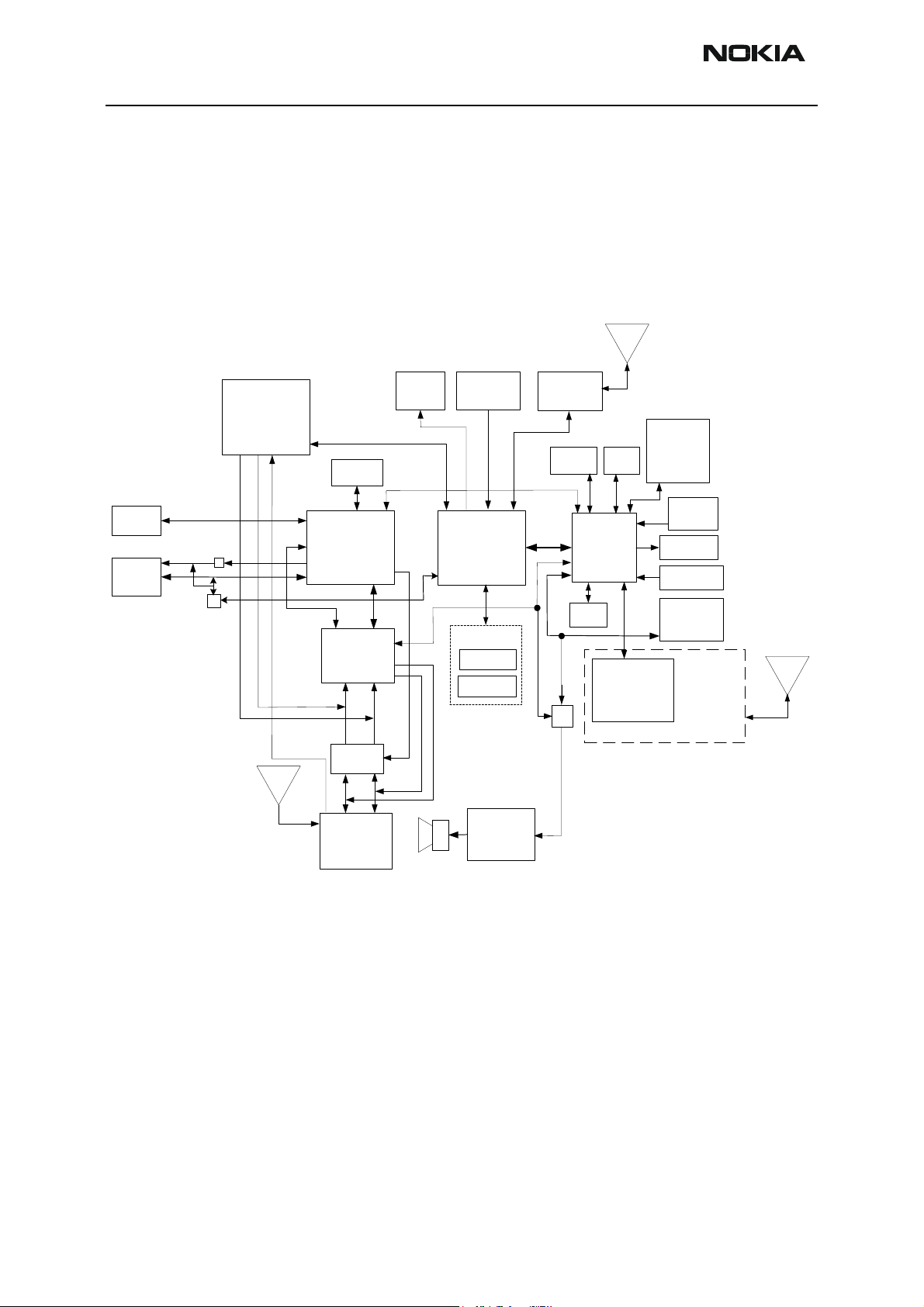
NEM-4 Block Diagram
NEM-4 product consists of RF, BB, Bluetooth and audio blocks.
External interfaces of NEM-4 consist of Bluetooth, stereo and mono headsets, charger as
well as the Universal Serial Bus (USB).
Figure 1: NEM-4 Block Diagram
Bluetooth
Antenna
USB
MMC
Nectar FM
radio chip
Radio out L
USB bus
Buffer
MMCclk
MMC bus (cmd,Data)
Lester
FM
Antenna
(Located in Stereo
Headset cable)
Radio out R
RF in
2
I
C bus
3-wire bus
FLASH
Amadeus
Digital Audio
Audio
codec
Stereo
Direction
switch
Stereo
Headset /
LIne In
(2,5 mm jack)
Display Keyboard
Amadeus-WD2 bus (level shifting in UEM)
McBSP
WD2
<- XEAR
MIC3 ->
Memories
FLASH
Control
Loudspeaker
SDRAM
Amplifier
<- XEAR
Bluetooth
Battery
Vibra
<- HF
<- HFCM
+
Mono
SIM
UEM
MJOELNER
Testpoints:
FBUS
MBUS
USB
FM radio
Battery
Charging
(DC jack)
Earpiece
Microphone
Mono
Headset
(2,5mm jack)
RF parts
Baseband Technical Summary
Baseband is basically constructed around three main ASICs or chips: UPP_WD2 (engine
ASIC with MCU, DSP and Digital Control Logic), UEM (handles e.g. power management,
charging and part of the external interfaces) and ADSP (audio processing). Discrete regulators are also used for powering.
Memory comprises of 3 x 64Mbit flash memory devices and 128Mbit (16Mbytes)
SDRAM.
For data connectivity there are Bluetooth, USB and MMC card.
The display is an MD-TFD LCD panel module with 4096 colours and 176x208 pixels with
backlighting. The keypad is a gaming keypad with a rocker and shortcut keys.
Page 7-6 Copyright © 2004 Nokia Corporation. Issue 2 09/2004
Company Confidential
Page 7

Company Confidential NEM-4
Nokia Customer Care 7 - Baseband
The audio part includes ADSP for audio processing and controlling, AIC audio codec and
Nectar FM radio chip. There are two audio transducers (Earpiece 8mm and IHF speaker
16mm) and external interface for stereo and mono headsets. The IHF speaker produces
the ring tone. The IHF speaker is driven by a discrete audio amplifier.
Functional Description
BB description
The BB core is based on UPP_WD2 CPU, which is a PDA version of the DCT4 UPP ASIC.
UPP_WD2 takes care of almost all of the signal processing and operation controlling
tasks of the phone as well as all PDA tasks. UPP_WD2 controls also controls ADSP and
Nectar audio chips. ADSP handles MP3 processing, USB-MMC functionality and AIC control.
UPP_WD2-ADSP data transmission is implemented with asynchronous two-signal bus,
routed via level shifter in UEM ASIC. Nectar FM-radio chip is controlled by UPP_WD2 via
I2C bus.
For power management there is one main ASIC for controlling charging and supplying
power UEM plus some discrete power supplies. The main reset for the system is generated by the UEM.
The interface to the RF and audio sections is also handled by the UEM. This ASIC provides
A/D and D/A conversion of the in-phase and quadrature receive and transmit signal
paths and also A/D and D/A conversions of received and transmitted audio signals. Data
transmission between UEM and RF and the UPP_WD2 is implemented using different
serial connections (CBUS, DBUS and RFBUS). Digital speech processing is handled by
UPP_WD2 ASIC.
A real time clock function is integrated into UEM, which utilizes the same 32kHz-clock
source as the sleep clock. A rechargeable battery provides backup power to run the RTC
when the main battery is removed. RTC Backup time is 7 hours.
Memory configuration
NEM-4 uses two kinds of memories, flash and SDRAM. These memories have their own
dedicated bus interfaces to UPP_WD2. The SDRAM size is 128Mbits (4M x 16).
Synchronous DRAM is used as working memory. Interface is 16 bit wide data and 14 bit
Address. Memory clocking speed is 104 MHz.
All memory contents are lost if the supply voltage is switched off.
Multiplexed flash memory interface is used to store the MCU program code and user
data. The memory interface is a burst type FLASH with multiplexed address/data bus,
running at 104/3MHz.
SDRAM I/O and core are supplied 1.8V bu UEM regulator VIO and discrete regulator
Issue 2 09/2004 Copyright © 2004 Nokia Corporation. Page 7-7
Company Confidential
Page 8

NEM-4 Company Confidential
7 - Baseband Nokia Customer Care
VMEMA respectively.
Energy management
The master of EM control is UEM and with SW this has the main control of the system
voltages and operating modes.
Modes of operation
NEM-4 employs several hardware & SW controlled operation modes. Main modes are
described below.
• NO_SUPPLY mode means that the main battery is not present or its voltage is too
low (below UEM master reset threshold) and back-up battery voltage is too low.
• In BACK_UP mode the main battery is not present or its voltage is too low but
back-up battery has sufficient charge in it.
• In PWR_OFF mode the main battery is present and its voltage is over UEM master
reset threshold. All regulators are disabled.
• RESET mode is a synonym for start-up sequence and contains in fact several
modes. In this mode regulators and oscillators are enabled and after they have
stabilized system reset is released and PWR_ON mode entered.
• In PWR_ON mode SW is running and controlling the system.
• SLEEP mode is entered from PWR_ON mode when the system’s activity is low
(SLEEPX controlled by SW).
• FLASHING mode is for production SW download.
Voltage limits
In the following the voltage limits of the system are listed. These are also controlling system states.:
Parameter Description Value
V
MSTR+
V
MSTR-
V
COFF+
Master reset threshold (rising) 2.1 V (typ.)
Master reset threshold (falling) 1.9 V (typ.)
Hardware cutoff (rising) 3.1 V (typ.)
V
COFF-
V_BU
V_BU
SW
COFF
COFF+
COFF-
Hardware cutoff (falling) 2.8 V (typ.)
Back-up battery cutoff (rising) 2.1 V (typ.)
Back-up battery cutoff (falling) 2.0 V (typ.)
SW cutoff limit (> regulator drop-out limit) MIN! 3.4 V SW changeable
Page 7-8 Copyright © 2004 Nokia Corporation. Issue 2 09/2004
Company Confidential
Page 9

Company Confidential NEM-4
Nokia Customer Care 7 - Baseband
The master reset threshold controls the internal reset of UEM. If battery voltage is above
V
, UEM’s charging control logic is alive. Also, RTC is active and supplied from the
MSTR
main battery. Above V
UEM allows the system to be powered on although this may
MSTR
not succeed due to voltage drops during start-up. SW can also consider battery voltage
too low for operation and power down the system.
Clocking scheme
A 26 MHz VCXO is used as system clock generator in GSM. During the system start-up,
UEM RC-oscillators generate timing for state machines. All clock signals of the engine
are illustrated in following figure.
Bluetooth uses 26 MHz clock.
Figure 2: NEM-4 Clocking.
Audio
12MHz
Oscillator
VCXO
26MHz
Clock
Amadeus
Audio
Codec
Buffer
MMC Clock
MMC
Nectar
FM Clock
Mjoelner
SysClk
Bluetooth
RFClk
RFBusClk
SDRClk
SDRAM
RFConvClock
SIM Clock
UPPWD2 UEM
Flash
Clock
DBus Clock
Sleep Clock
CBus Clock
SIM
Clock
SIMZocusFlash
In SLEEP mode the VCXO is off. UEM generates low frequency clock signal (32.768 kHz)
that is fed to UPP_WD2, Bluetooth and ZOCUS.
ADSP and AIC use a 12 MHz clock (audio clock) generated by external oscillator. The
Audio clock is on when ADSP is powered.
UPP_WD2 voltage/clock frequency adjusting
No external clock is available for UPP_WD2 before VCXO starts. As reset is released, the
VCXO is running and MCU uses the 26 MHz clock while DSP is in reset. There are three
identical DPLL's, for MCU, for DSP and for accessory interfaces, which can be controlled
Issue 2 09/2004 Copyright © 2004 Nokia Corporation. Page 7-9
Company Confidential
Page 10

NEM-4 Company Confidential
7 - Baseband Nokia Customer Care
independently. The clock for MCU can be up to 104 MHz and 117 MHz is maximum clock
Frequency for the DSP. These clock signals are used either directly (SDRAM IF) or divided
down for the interfaces (e.g. flash IF).
Power distribution, control and reset
All power (except backup battery power) is drawn from BL5-C Li-Ion battery located in
the B cover. Current flows through ZOCUS current sense resistor which is used for current measurement by ZOCUS and thus for remaining operating time estimation.
EM4 board contains one power ASIC, UEM and discrete regulators needed for generating
the different operating voltages. The discrete regulators consist of two SMPSs and four
linear regulators. Two SMPSs are used to power UPP_WD2 core voltage and SDRAM core
voltage. Three linear regulators power 3.1V for ADSP and AIC audio converter. One 1.5V
linear regulator is used for ADSP core voltage. In addtion there is a SMPS in EM4 generating the operating voltage for display module backlighting.
Power-up sequence (reset mode)
RESET mode can be entered in four ways: by inserting the battery or charger, by RTC
alarm or by pressing the power key. The VCXO is Powered by UEM. After a 220 ms delay
regulators are configured and UEM enters PWR_ON mode and system reset PURX is
released.
During system start-up, in RESET state, the regulators are enabled, and each regulator
charges the capacitor(s) at the output with the maximum current (short circuit current)
it can deliver. This results in battery voltage dropping during start-up. When a battery
with voltage level just above the hardware cutoff limit is inserted, the system may not
start due to excessive voltage dipping. Dropping below 2.8 V for longer than 5 us forces
the system to PWR_OFF state.
Powering off
Controlled powering off is done when the user requests it by pressing the power key or
when the battery voltage falls too low. Uncontrolled powering off happens when the
battery is suddenly removed or if over-temperature condition is detected in regulator
block while in RESET mode. Then all UEM’s regulators are disabled immediately and discrete regulators are disabled as Vbat supply disappears.
Controlled powering off
For NEM-4 powering off is initiated by pressing the power key and Power off sequence is
activated in UEM and SW. Basically, the power key causes UEM interrupt to UPP_WD2
and SW sets the watchdog time value to zero and as this happens, PURX is forced low
and all regulators are disabled.
If the battery voltage falls below the very last SW-cutoff level, SW will power off the
system by letting the UEM’s watchdog elapse.
If thermal shutdown limit in UEM regulator block is exceeded, the system is powered off.
System reset PURX is forced low.
Page 7-10 Copyright © 2004 Nokia Corporation. Issue 2 09/2004
Company Confidential
Page 11

Company Confidential NEM-4
Nokia Customer Care 7 - Baseband
Uncontrolled powering off
This happens when the battery is suddenly removed. UEM’s state machine notices battery
removal after battery voltage has been below V
PURX is set low and all UEM’s regulators are disabled.
Watchdogs
There are three watchdogs in UEM. The first one is for controlling system power-on and
power-down sequences. The initial time for this watchdog after reset is 32 s and the
watchdog can not be disabled. The time can be set using a register. This watchdog is used
for powering the system off in a controlled manner. The other one is for security block
and is used during IMEI code setting. The third one is a power key watchdog. It is used to
power off the system in case SW is stuck and the user presses the power key. This WD is
SW configurable.
There is also a ”soft watchdog” in UPP_WD2. It is used to reset the chip in case software
gets stuck for any reason. The Bluetooth module also contains a watchdog.
for 5 us and enters PWR_OFF mode.
COFF-
Charging
Charging control and charge switch is in UEM. There are two different charging modes;
charging empty battery (start-up charge mode), and SW controlled charging.
UEM digital part takes care of charger detection (generates interrupt to UPP_WD2),
pulse width modulated charging control (for internal charge switch) and over voltage
and current detection. SW using registers controls all these.
Chargers
NEM-4 BB supports a standard charger (two wires), chargers ACP-8 and ACP-12, cigarette charger LCH-8 and LCH-12 are supported.
Battery
NEM-4 battery is a detachable, semi-fixed Lithium-Ion BL5-C battery. Nominal voltage is
thus 3.7 V (max charging voltage 4.2 V).
The interface consists of three pins: VBAT, GND and BSI. Pull-down resistor inside of the
batteries (BSI signal) recognizes the battery types. Voltage level at BSI line is measured
using UEM's AD-converter.
Back-up battery and real time clock
Real time clock (RTC), crystal oscillator and back-up battery circuitry reside in UEM. A
register in UEM controls back-up battery charging and charging is possible only in
POWER_ON State.
Baseband measurement A/D converter
UEM contains 11 channels A/D converter, which is used for different baseband measurement purposes. The resolution of A/D converter is 10 bits. Converter uses the CBUS interface clock signal for the conversion. An interrupt will be given to the MCU at the end of
Issue 2 09/2004 Copyright © 2004 Nokia Corporation. Page 7-11
Company Confidential
Page 12

NEM-4 Company Confidential
7 - Baseband Nokia Customer Care
the measurements. The Converter is used for following purposes.
• Battery Voltage Measurement A/D Channel (Internal)
• Charger Voltage Measurement A/D Channel (Internal)
• Charger Current Measurement A/D Channel (Internal)
• Battery Temperature Measurement A/D Channel (External)
• Battery Size Measurement A/D Channel (External)
• LED Temperature measurement A/D Channel (External)
There is also auxiliary AD converter in UEM, which is used to monitor RF functions.
ZOCUS
The ZOCUS device is a current sensor used for the battery bar display and for determining
whether the phone is in a high current consuming mode. The ZOCUS device measures the
voltage drop across a sense resistor in the battery voltage line. This sense resistor is
formed from a PWB track and is on an internal layer of the PWB. The sense resistor must
be located close to the battery terminals so that all of the phones current flow through
it. The nominal value of the sense resistor is 3.3 mohm. ZOCUS reports the current measurement to UPP_WD2 via the Cbus interface.
NEM-4 BB Features, HW Interfaces and User Interface
Display and keypad
The UI-module consists of the LCD and keymat. The NEM-4 display resolution is 176 x
208 and backlighting is via 4 white LEDs with lightguide. The display is connected to
EM4 board with 16-pin connector. The keypad is of gaming type and is backlighted with
10 LEDs. The keymat interfaces with UPP_WD2 GPIO/GENIO pins.
Bluetooth
Bluetooth provides a fully digital link for communication between a master unit and one
or more slave units. The system provides a radio link that offers a high degree of flexibility to support various applications and product scenarios. Data and control interface for
a low power RF module is provided. Data rate is regulated between the master and the
slave.
SIM interface
The SIM interface is located in two chips (UPP_WD2 and UEM). In UEM there is only support for one SIM card. The interfaces support both 1.8 V and 3 V SIM cards. Adjustable
SIM regulator (1.8V/3.0V) is located in UEM and can be controlled by SW.
The data communication between the card and the phone is asynchronous half duplex.
Page 7-12 Copyright © 2004 Nokia Corporation. Issue 2 09/2004
Company Confidential
Page 13

Company Confidential NEM-4
Nokia Customer Care 7 - Baseband
The clock supplied to the card is 3.25 MHz. The data baudrate is SIM card clock frequency divided by 372 (by default), 64, 32 or 16.
MMC interface
MMC is interfaced with UPP_WD2 and ADSP. Both UPP_WD2 and ADSP have MMC
interfacing functionality integrated to the chip. The MMC interface comprises of three
lines: clock, data and command and runs at 8.66MHz. There is EMC protection ASIP for
MMC as well as a level shifter (Lester) for UPP_WD2 MMC signals and a buffer for ADSP
MMC clock line. The Lester device also incorporates a 2.85V regulator to the MMC card.
NEM-4 audio concept
NEM-4 audio includes earpiece, microphone, stereo headset connector, Mono headset
connector, Integrated Handsfree (IHF). Audio is based on UPPWD2 phone engine ASIC,
ADSP Application DSP, AIC Audio Codec, Nectar FM Radio and several discrete components including amplifier for IHF called Boomer.
Also UEM ASIC is used for many audio tasks. NEM-4 audio block diagram is presented in
figure below.
Figure 3: NEM-4 Audio Block Diagram.
ADSP
The Application DSP (ADSP) is responsible for MP3/AAC decoding, AAC encoding, play-
Issue 2 09/2004 Copyright © 2004 Nokia Corporation. Page 7-13
Company Confidential
Page 14

NEM-4 Company Confidential
7 - Baseband Nokia Customer Care
back and recording the audio data stream as well as equalizing the playback from MP3/
AAC audio data and FM radio. This part generates the ringing tones and controls the
ringing tone power amplifier.
Audio routing and conditioning
The analog audio sources, FM radio and line in, are mixed and level conditioned in a passive stereo mixer and then fed through the Audio Codec RLINEIN and LLINEIN. The GSM
downlink from the UEM HFOUT for headset is routed through the codec mono analog
input (MICIN).
Source selection is controlled by software using the mute function for GSM downlink
and power on/off for FM radio. FM radio is powered off when not in use for power saving. Disabling the output stage of the UEM mutes the GSM downlink signal. Line in signal is the master signal and cannot be muted.
Stereo headset detection is done via sense line from the 2.5mm jack connector to
UPP_WD2 GENIO22.
The amplification and routing of the analog audio sources and outputs of the audio
codec (AIC) is done via the control interface (SDIN, SCLK, CS, MODE) and the digital
audio interface (DIN, LRCOUT, DOUT, BCLK) from ADSP.
Audio signal routing is done by software. The hardware concept is fixed wired. Only
exception is the direction switch, that is used route line in audio from Stereo HS to AIC,
and to route FM radio signal via AIC when radio is listened. Direction switch is controlled
by ADSP GPIO6. The software manages the sources/inputs and the outputs that will be
connected for the used path. Level and volume control, the equalizing for the selected
path etc. are also controlled by software.
When recording from FM radio or line in, the signal can be monitored via IHF. A phone
call during recording is not possible.
The following sections give an overview of the audio use cases.
FM radio play
In this case, AIC is doing the AD and the DA conversions and ADSP is responsible for gain
setting and equalizing functions.
FM radio/line in recording
In this case, ADSP is responsible for encoding the digital audio signal. If the FM radio is
chosen as source, the gain setting by 12dB is done by ADSP as well.
MP3/AAC playback
In this case, ADSP is working as decoder for digital audio stored on the MMC.
GSM audio handsfree mode
In handsfree mode, only the PA in the codec is used to drive the headset. The external
Page 7-14 Copyright © 2004 Nokia Corporation. Issue 2 09/2004
Company Confidential
Page 15

Company Confidential NEM-4
Nokia Customer Care 7 - Baseband
audio PA (Boomer) will be activated if the IHF loudspeaker is used for IHF mode.
Standard ringing tones / alarm tones
The routing for playing ringing or alarm tones is the same like in GSM handsfree mode.
MP3/AAC/MIDI ringing tones
If MP3/AAC files are used as ringingtone, the routing corresponds to the routing in MP3/
AAC playback mode.
MultiMediaCard MMC
NEM-4 uses a MMC as memory for the MP3/AAC files as well as games and other multimedia files. Records from line in or FM radio can be saved on this card. Also music files
via USB can be stored on the MMC. The MMC is located under the battery and can be
easily changed by the end user.
MMC can be accessed by both ADSP and UPPWD2. MMC interface includes CLK, CMD
and DAT0 lines.
MMC power is supplied by additional 2.8V regulator integrated on same package with
MMC level shifter (Lester). Lester does the level shifting for UPPWD2-MMC signals, and
is controlled by UPPWD2 ASIC.
MMC CLK line between ADSP and MMC is buffered and the buffer is controlled by UEM.
ADSP flash memory
ADSP code and data is stored in a 16Mb, 16 bit wide asynchronous flash memory.
Acoustics
The following chapters give a description of acoustical parts.
Earpiece
The internal earpiece is a dynamic earpiece with an impedance of 32 ohms. The earpiece
is low impedance one since the sound pressure is to be generated using current and not
voltage as the supply voltage is limited to 2.7V.
The earpiece is driven directly by the UEM and the earpiece driver in UEM is a bridge
amplifier.
Microphone
The internal microphone capsule is embedded into the chassis. Microphone is omnidirectional. The internal microphone is connected to the UEM microphone input MIC1P/N. The
microphone input is asymmetric and microphone bias is provided by the UEM MIC1B. The
microphone input on the UEM is ESD protected. Spring contacts are used to connect the
microphone contacts to the engine PWB.
Loudspeaker
The loudspeaker in NEM-4 is used to generate alerting, ringing and warning tones. It is
Issue 2 09/2004 Copyright © 2004 Nokia Corporation. Page 7-15
Company Confidential
Page 16

NEM-4 Company Confidential
7 - Baseband Nokia Customer Care
also used as Integrated Handsfree (IHF) Speaker and as speaker for media playbac (MP3,
AAC, FM Radio).
Speaker capsule is embedded into the chassis. Spring contacts are used to connect the
speaker contacts to the engine PWB.
Headset
The headset is of passive type with mono and stereo connectors as well as integrated
microphone with answer key. The type name is HDD-2.
FM radio
The FM radio in NEM-4 is a single chip electronically tuned FM stereo radio with fully
integrated IF selectivity and demodulation. It can be tuned to European, US and Japanese
FM bands. The channel tuning and bus data are controlled by UPP via I2C bus (SDA, SCL
and W/R signals). FM radio is only working when headset is connected because the cable
is used as FM antenna.
Flashing
SW download in service is implemented by custom tools and SW, kindly refer to Service
Software Instructions and Service Tool section of the manual.
Page 7-16 Copyright © 2004 Nokia Corporation. Issue 2 09/2004
Company Confidential
Page 17

Company Confidential NEM-4
Nokia Customer Care 7 - Baseband
Testing interfaces
Testing interface electrical specifications
Pin Name Dir Parameter Min Typ Max Unit Notes
1 MBUS <-> Vol 0 0.2 0.3*VFlash1 V
Vil (From Prommer) 0 0.2 0.3*VFlash1 V
Voh 0.7*VFlash1 2.7 0.7*VFlash1 V
Vih(From Prommer) 0.7*VFlash1 2.7 VFlash1 V
2 FBusTx -> Vol 0 2.7 0.3*VFlash1 V
Voh 0.7*VFlash1 2.7 VFlash1 V
3 FBusRx <- Vil (From Prommer) 0 2.7 0.3*VFlash1 V
Vih(FromPrommer) 1.89 2.7 VFlash1 V
Abs. Max. Voltage
to Test Pad Referenced to GND
4 VPP To Phone 0 / 2.8 / 12 +/-3% V Prommer
4 VPP To Phone 0 / 2.8 / 12 +/-3% V Prommer
5 GND 0 V VBAT
-0.3V 3.0 V Absolute Max
Voltage limits
to MBUS/
FBUS
4 VPP
Select
4 VPP
Select
GROUND
Note1: VFlash1 is 2.78 +/- 3%
Electrical specifications for power supply interface in prod testing
Pin Name Min Typ Max Unit Notes
1 VBAT 0 3.6 5.1 V
2 BSI 0 2.78 VFlash1 V Internal pullup
3 GND 0 V
Note 1: VAna & VFlash1 = 2.78 +/-3%
Issue 2 09/2004 Copyright © 2004 Nokia Corporation. Page 7-17
Company Confidential
Page 18

NEM-4 Company Confidential
7 - Baseband Nokia Customer Care
Extreme voltages
Lithium-Ion battery BL-5C (1 cell):
Nominal voltage is 3.7V
Lower extreme voltage is 2.8V (cut off voltage)
Higher extreme voltage is 4.2V (charging high limit voltage)
Temperature conditions
Specifications are met within range of –10C to +55C ambient temperature. Reduced
operation between [-30] and [+60]. Storage temperature range is of –40C to +85C.
Humidity and water resistance
Relative humidity range is 5 … 95%. Condensed or dripping water may cause intermittent malfunctions. Protection against dripping water has to be implemented in (enclosure) mechanics. Continuous dampness will cause permanent damage to the module.
Page 7-18 Copyright © 2004 Nokia Corporation. Issue 2 09/2004
Company Confidential
 Loading...